
Related Manuals for Texas Instruments TPS54373EVM-237


Summary of Contents for Texas Instruments TPS54373EVM-237
- Page 1 TPS54373EVM 237 3 Amp SWIFT Regulator With Disabled Sink During Start Up Evaluation Module User’s Guide June 2003 PMP Systems Power SLVU088...
- Page 2 TI product or service and is an unfair and deceptive business practice. TI is not responsible or liable for any such statements. Following are URLs where you can obtain information on other Texas Instruments products & application solutions:...
- Page 3 EVM IMPORTANT NOTICE Texas Instruments (TI) provides the enclosed product(s) under the following conditions: This evaluation kit being sold by TI is intended for use for ENGINEERING DEVELOPMENT OR EVALUATION PURPOSES ONLY and is not considered by TI to be fit for commercial use. As such, the goods being provided may not be complete in terms of required design-, marketing-, and/or manufacturing-related protective considerations, including product safety measures typically found in the end product incorporating the goods.
- Page 4 EVM schematic located in the EVM User’s Guide. When placing measurement probes near these devices during operation, please be aware that these devices may be very warm to the touch. Mailing Address: Texas Instruments Post Office Box 655303 Dallas, Texas 75265 Copyright 2003, Texas Instruments Incorporated...
- Page 5 A caution statement describes a situation that could potentially damage your software or equipment. This is an example of a warning statement. A warning statement describes a situation that could potentially cause harm to you. Related Documentation From Texas Instruments TPS54373 data sheet (literature number SLVS455)
- Page 6 Information About Cautions and Warnings Trademarks SWIFT is a trademark of Texas Instruments. PowerPAD is a trademark of Texas Instruments.
-
Page 7: Table Of Contents
Contents Contents Introduction ..............Background . - Page 8 ........1–2 TPS54373EVM-237 Performance Specification Summary ......
-
Page 9: Introduction
Introduction This chapter contains background information for the TPS54373 as well as support documentation for the TPS54373EVM-237 evaluation module (SLVP237). The TPS54373EVM-237 performance specifications are given, with the schematic and bill of material for the TPS54373EVM-237. Topic Page Background .......... -
Page 10: Background
Background 1.1 Background The TPS54373EVM-237 evaluation module uses the TPS54373 synchronous buck regulator with disabled sink during start-up (DSDS) to provide an output voltage of from 0.9 V to 2.5 V from a nominal 3.3-V input or 0.9 V to 3.3 V for a nominal 5-V input. -
Page 11: Performance Specification Summary
J4. Using the precharge circuitry on this EVM requires careful consideration of line and load conditions for proper operation and may limit the useful operating range of the TPS54373 device. Table 1–2. TPS54373EVM-237 Performance Specification Summary Specification Test Conditions Units 3.3 or... -
Page 12: Modifications
Modifications 1.3 Modifications The TPS54373EVM-237 is designed to demonstrate the small size that can be attained when designing with the TPS54373, so many of the features, which allow for extensive modifications have been omitted from this EVM. Changing the value of R2 can change the output voltage in the range of 0.9 V to 3.3 V. -
Page 13: Frequency Trimming Resistor Selection Graph
I/O voltage minus the drop across the diodes during start-up. The TPS54373EVM-237 EVM provides four series diodes, D1 through D4, and allows the user to precharge the output from either the EVM input voltage or an external source. - Page 14 Modifications Warning Under no circumstances can the output voltage be allowed to precharge to a level higher than the preset output voltage. If this condition occurs during start-up, the TPS54373 device does not begin switching. If a voltage transient on the precharge voltage source causes the series diodes to conduct, current may be sunk through the low side FET in the device, possibly damaging the device.
-
Page 15: Test Setup And Results
Test Setup and Results This chapter describes how to properly connect, setup, and use the TPS54373EVM-237 evaluation module. The chapter also includes test results typical for the TPS54373EVM-237 and covers efficiency, output voltage regulation, load transients, loop response, output ripple, input ripple, and start-up. -
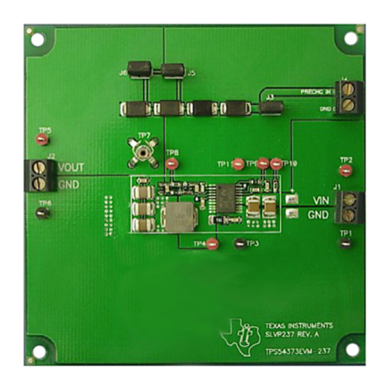
Page 16: Input/Output Connections
The TPS54373 is intended to be used as a point of load regulator. In typical applications it is usually located close to the input voltage source. When using the TPS54373EVM-237 with an external power supply as the source for , an additional bulk capacitor may be required, depending upon the output impedance of the source and length of the hookup wires. -
Page 17: Efficiency
Efficiency 2.2 Efficiency The TPS54373EVM-237 efficiency peaks at load current of about 1 A to 2 A, and then decreases as the load current increases towards full load. Figure 2–2 shows the efficiency for the TPS54373 at an ambient temperature of 25°C. The efficiency is lower at higher ambient temperatures, due to temperature variation in the drain-to-source resistance of the MOSFETs. -
Page 18: Power Dissipation
Power Dissipation 2.3 Power Dissipation The low junction-to-case thermal resistance of the PWP package, along with a good board layout, allows the TPS54373EVM–237 EVMs to output full rated load current while maintaining safe junction temperatures. With a 3.3-V input source and a 3-A load, the junction temperature is approximately 60°C, while the case temperature is approximately 55°C. -
Page 19: Output Voltage Regulation
Output Voltage Regulation 2.4 Output Voltage Regulation The output voltage load regulation of the TPS54373EVM-237 is shown in Figure 2–4, while the output voltage line regulation is shown in Figure 2–5. Measurements are given for an ambient temperature of 25°C. -
Page 20: Load Transients
Load Transients 2.5 Load Transients The TPS54373EVM-237 response to load transients is shown in Figure 2–6. The current step is from 25% to 75% of maximum rated load. Total peak-to-peak voltage variation is as shown, including ripple and noise on the output. -
Page 21: Loop Characteristics
Loop Characteristics 2.6 Loop Characteristics The TPS54373EVM-237 loop response characteristics are shown in Figure 2–7 and Figure 2–8. Gain and phase plots are shown for each device at minimum and maximum operating voltage. Figure 2–7. Measured Loop Response, TPS54373, V... -
Page 22: Output Voltage Ripple
Output Voltage Ripple 2.7 Output Voltage Ripple The TPS54373EVM–237 output voltage ripple is shown in Figure 2–9. The input voltage is 3.3 V for the TPS54373. Output current is the rated full load of 3 A. Voltage is measured directly across output capacitors. Figure 2–9. -
Page 23: Input Voltage Ripple
Input Voltage Ripple 2.8 Input Voltage Ripple The TPS54373EVM–237 output voltage ripple is shown in Figure 2–10. The input voltage is 3.3 V for the TPS54373. Output current for each device is rated full load of 3 A. Figure 2–10. Input Voltage Ripple, TPS54373 V O (ac) 20 mV/div V phase 1 V/div Time Scale 1 µs/div... -
Page 24: Start-Up
Start-Up 2.9 Start-Up Start-up voltage waveforms of the TPS54373EVM–237 are shown in Figure 2–11 through Figure 2–15. Figure 2–11 shows the start-up waveform with no precharge on the output. When the V reaches the nominal 2.95-V UVLO threshold, the slow start capacitor C5 begins to charge. When the voltage on the SS/ENA pin reaches the enable threshold of 1.2 V, the internal reference begins to ramp up at the slow start rate. -
Page 25: Measured Start-Up Waveform, Two Diode Precharge
Start-Up Figure 2–12. Measured Start-Up Waveform, Two Diode Precharge V I 500 mV/div V O 500 mV/div Time Scale 5 ms/div Figure 2–13. Measured Start-Up Waveform, Three Diode Precharge V I 500 mV/div V O 500 mV/div Time Scale 5 ms/div Test Setup and Results 2-11... -
Page 26: Measured Start-Up Waveform, Four Diode Precharge
Start-Up Figure 2–14. Measured Start-Up Waveform, Four Diode Precharge V I 500 mV/div V O 500 mV/div Time Scale 5 ms/div Figure 2–15 shows the start-up waveform with the output precharged through 4 diodes and no load. Compare the precharge level to that in Figure 2–14 to see how start-up load current affects the voltage drop across the diodes and the final precharge voltage. -
Page 27: Measured Start-Up Waveform, Four Diode Precharge And No Load
Start-Up Figure 2–15. Measured Start-Up Waveform, Four Diode Precharge and No Load V I 500 mV/div V O 500 mV/div Time Scale 5 ms/div Test Setup and Results 2-13... - Page 28 2-14...
-
Page 29: Board Layout
Chapter 3 Board Layout This chapter provides a description of the TPS54373EVM–237 board layout and layer illustrations. Topic Page Layout ............Board Layout... -
Page 30: Layout
3.1 Layout The board layout for the TPS54373EVM-237 is shown in Figure 3–1 through Figure 3–3. The top-side layer of the TPS54373EVM-237 is laid out in a manner typical of a user application. The bottom layer of the TPS54373EVM-237 is designed to accommodate optional alternate output filter capacitors. -
Page 31: Bottom-Side Layout (Looking From Top Side)
Layout Figure 3–2. Bottom-Side Layout (looking from top side) Figure 3–3. Top-Side Assembly Board Layout... -
Page 33: Schematic And Bill Of Materials
Chapter 4 Schematic and Bill of Materials The TPS54373EVM–237 schematic and bill of materials are presented in this chapter. Topic Page Schematic ........... . Bill of Materials . -
Page 34: Schematic
Schematic 4.1 Schematic The schematic for the TPS54373EVM–237 is shown in Figure 4–1. Figure 4–1. TPS54373EVM–237 Schematic 10 µF TPS54373PWP PRECHG_IN AGND VSENSE SYNCH TP11 COMP SS/ENA PWRGD VBIAS 6.34 kΩ 1500 pF BOOT MURS120T3 1 µF 0.047 µF 71.5 kΩ 0.047 µF PGND 82 pF... -
Page 35: Bill Of Materials
Bill of Materials 4.2 Bill of Materials Table 4–1 contains the bill of materials for the TPS54380EVM–001. Table 4–1. TPS54373EVM-237 Bill of Materials Count RefDes Description Size Part Number Capacitor, POSCAP, 220 µF, 10 V, 40 mΩ, 20% Sanyo 10TPB220M Capacitor, ceramic, 0.1 µF, 25 V, X7R, 10%...
Need help?
Do you have a question about the TPS54373EVM-237 and is the answer not in the manual?
Questions and answers