
Subscribe to Our Youtube Channel
Related Manuals for Texas Instruments TPS54673EVM-225


Summary of Contents for Texas Instruments TPS54673EVM-225
- Page 1 TPS54673EVM 225 6 Amp TPS54873EVM 225 8 Amp SWIFT Regulator With Disabled Sink During Start Up Evaluation Module User’s Guide January 2003 PMP EVMs SLVU079...
- Page 2 IMPORTANT NOTICE Texas Instruments Incorporated and its subsidiaries (TI) reserve the right to make corrections, modifications, enhancements, improvements, and other changes to its products and services at any time and to discontinue any product or service without notice. Customers should obtain the latest relevant information before placing orders and should verify that such information is current and complete.
- Page 3 EVM IMPORTANT NOTICE Texas Instruments (TI) provides the enclosed product(s) under the following conditions: This evaluation kit being sold by TI is intended for use for ENGINEERING DEVELOPMENT OR EVALUATION PURPOSES ONLY and is not considered by TI to be fit for commercial use. As such, the goods being provided may not be complete in terms of required design-, marketing-, and/or manufacturing-related protective considerations, including product safety measures typically found in the end product incorporating the goods.
- Page 4 EVM schematic located in the EVM User’s Guide. When placing measurement probes near these devices during operation, please be aware that these devices may be very warm to the touch. Mailing Address: Texas Instruments Post Office Box 655303 Dallas, Texas 75265 Copyright 2003, Texas Instruments Incorporated...
- Page 5 Information About Cautions and Warnings Preface Read This First About This Manual This user’s guide describes the characteristics, operation, and use of the TPS54673EVM–225 and TPS54873EVM–225 evaluation modules. It covers all pertinent areas involved to properly use this EVM board along with the de- vices that it supports.
- Page 6 Trademarks TI Logo is a trademark of Texas Instruments Incorporated. PowerPAD is a trademark of Texas Instruments Incorporated.
-
Page 7: Table Of Contents
Contents Contents Introduction ..............Background . - Page 8 Contents Figures 1–1 Frequency Trimming Resistor Selection Graph ........2–1 Connection Diagram .
- Page 9 ........1–2 TPS54673EVM-225 Performance Specification Summary ......
-
Page 11: Introduction
Chapter 1 Introduction This chapter contains background information for the TPS54673 and TPS54873, as well as support documentation for the TPS54673EVM-225 and TPS54873EVM-225 evaluation modules (SLVP225). The TPS54x73EVM-225 performance specifications, schematic, and bill of materials are given. Topic Page Background . -
Page 12: Background
I/O and core voltages during start-up. Table 1–1. Input Voltage and Output Current Summary Input Voltage Range Output Current Range TPS54673EVM-225 3.0 V to 6.0 V –6 A to 6 A TPS54873EVM-225 4.0 V to 6.0 V –8 A to 8 A... -
Page 13: Tps54673Evm-225 Performance Specification Summary
Performance Specification Summary Table 1–2. TPS54673EVM-225 Performance Specification Summary Specification Test Conditions Units 3.3 or Input voltage range Output voltage set point Output current range = 3 V to 6 V ±4 Line regulation (see Note 1) = 3 A, V = 3.02 V to 6 V... -
Page 14: Modifications
Modifications 1.3 Modifications The TPS54x73EVM-225 is designed to demonstrate the small size that can be attained when designing with the TPS54x73, so many of the features which allow for extensive modifications have been ommited from this EVM. Changing the value of R4 can change the output voltage in the range of 0.9 V to 3.3 V. - Page 15 Modifications The TPS54x73EVM–225 EVM also supports alternate output filter configura- tions by means of pads located on the back side of the PCB. The positions for C15, C16, and C17 provide space for up to three electrolytic type surface, mount capacitors, while the position for L2 accommodates popular inductors such as Vishay IHLP-5050 series with a 0.5 in.
-
Page 17: Test Setup And Results
Chapter 2 Test Setup and Results This chapter describes how to properly connect, set up, and use the TPS54x73EVM-225 evaluation module. The chapter also includes test results typical for the TPS54x73EVM-225 and covers efficiency, output voltage regulation, load transients, loop response, output ripple, input ripple, and start-up. -
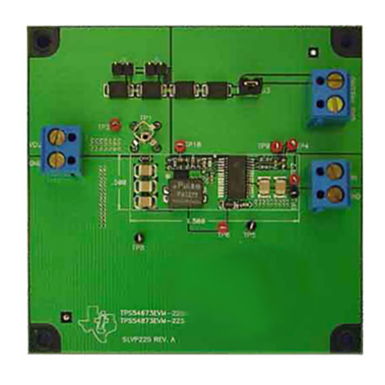
Page 18: Input/Output Connections
Input/Output Connections 2.1 Input/Output Connections The TPS54x73EVM-225 has the following input/output connections: Vout J1, Vin J2, and Prechg_in J4. A diagram showing the connection points is shown in Figure 2–1. A power supply capable of supplying 6 A should be connected to J2 through a pair of 20-AWG wires. -
Page 19: Efficiency
Efficiency 2.2 Efficiency The TPS54x73EVM-225 efficiency peaks at load current of about 1 A to 2 A, and then decreases as the load current increases towards full load. The efficiency shown in Figure 2–2 is for the TPS54673 and the TPS54873 at an ambient temperature of 25°C. -
Page 20: Measured Efficiency, Tps54873
Efficiency Figure 2–3. Measured Efficiency, TPS54873 EFFICIENCY OUTPUT CURRENT V I = 5 V, V O = 3.3 V I O – Output Current – A... -
Page 21: Power Dissipation
Power Dissipation 2.3 Power Dissipation The low junction-to-case thermal resistance of the PWP package, along with a good board layout, allows the TPS54x73EVM-225 EVMs to output full rated load current while maintaining safe junction temperatures. With a 3.3-V input source and a 6-A load, the junction temperature is approximately 60°C, while the case temperature is approximately 55°C. -
Page 22: Output Voltage Regulation
Output Voltage Regulation 2.4 Output Voltage Regulation The output voltage load regulation of the TPS54x73EVM-225 is shown in Figure 2–5, while the output voltage line regulation is shown in Figure 2–6. Measurements are given for an ambient temperature of 25°C. Figure 2–5. -
Page 23: Line Regulation
Output Voltage Regulation Figure 2–6. Line Regulation OUTPUT VOLTAGE INPUT VOLTAGE TPS54873 TPS54673 V I – Input Voltage – V Note: The lower limit for the TPS54673 input voltage is about 3.02 V because the device is operating at its maximum duty cycle. -
Page 24: Load Transients
Load Transients 2.5 Load Transients The TPS54x73EVM–225 response to load transients is shown in Figure 2–7 and Figure 2–8. The current step is from 25 to 75 percent of maximum rated load. Total peak-to-peak voltage variation is as shown, including ripple and noise on the output. -
Page 25: Loop Characteristics
Loop Characteristics 2.6 Loop Characteristics The TPS54x73EVM-225 load response characteristics are shown in Figure 2–9, Figure 2–10, and Figure 2–11. The current step is from –50% to 50% of maximum rated load. Total peak-to-peak voltage variation is as shown, including ripple and noise on the output. Figure 2–9. -
Page 26: Measured Loop Response, Tps54873, V I = 4 V
Loop Characteristics Figure 2–11. Measured Loop Response, TPS54873, V = 4 V MEASURED LOOP RESPONSE Gain Phase –30 –10 –20 –60 –90 –30 –120 –40 –50 –150 –180 –60 10 k 100 k f – Frequency – Hz Figure 2–12. Measured Loop Response, TPS54873, V = 6 V MEASURED LOOP RESPONSE Gain... -
Page 27: Output Voltage Ripple
Output Voltage Ripple 2.7 Output Voltage Ripple The TPS54x73EVM-225 output voltage ripple is shown in Figure 2–13 and Figure 2–14 for each device type. The input voltage is 3.3 V for the TPS54673. The input voltage is 5 V for the TPS54873. Output current for each device is the rated full load. -
Page 28: Input Voltage Ripple
Input Voltage Ripple 2.8 Input Voltage Ripple The TPS54x73EVM-225 input voltage ripple is shown in Figure 2–15 and Figure 2–16 for each device type. The input voltage is 3.3 V for the TPS54673 the input voltage is 5 V for the TPS54873. Output current for each device is the rated full load. -
Page 29: Start-Up
Start-Up 2.9 Start-Up Start-up voltage waveforms of the TPS54673EVM–225 are shown in Figure 2–17 through Figure 2–19. Figure 2–17 shows the start-up waveform with no precharge on the output. When the V reaches the nominal 2.95-V UVLO threshold, the slow-start capacitor (C6) begins to charge. When the voltage on the SS/ENA pin reaches the enable threshold of 1.2 V, the internal reference begins to ramp up at the slow-start rate. -
Page 30: Measured Start-Up Waveform, Tps54373 With Precharge
Start-Up Figure 2–18. Measured Start-Up Waveform, TPS54373 With Precharge V I 1 V/div V O 1 V/div Time Scale – 5 µs/div Figure 2–20 shows the start-up waveform with the output precharged and no load. Compare the precharge level to that in Figure 2–18 to see how start-up load current affects the voltage drop across the diodes and the final precharge voltage. -
Page 31: Measured Start-Up Waveform
Start-Up Figure 2–20, Figure 2–21, and Figure 2–22 show the same series start-up waveforms for the TPS54873-225. The above descriptions of the TPS54673 waveforms are applicable for the TPS54873 except that the input voltage is 5 V, the output voltage is 3.3 V, and the UVLO start-up threshold is 3.8 V. Figure 2–20. -
Page 32: Measured Start-Up Waveform, Tps54873 With Precharge And No Load
Start-Up Figure 2–22. Measured Start-Up Waveform, TPS54873 With Precharge and No Load V I 1 V/div V O 1 V/div Time Scale – 5 µs/div 2-16... -
Page 33: Board Layout
Chapter 3 Board Layout This chapter provides a description of the TPS54x73EVM-225 board layout and layer illustrations. Topic Page Layout ............Board Layout... -
Page 34: Layout
Layout 3.1 Layout The board layout for the TPS54x73EVM-225 is shown in Figure 3–1 through Figure 3–6. The top-side layer of the TPS54x73EVM-225 is laid out in a manner typical of a user application. The bottom layer of the TPS54x73EVM-225 is designed to accommodate an optional alternate output filter configuration. -
Page 35: Internal Layer 1 Layout
Layout Figure 3–2. Internal Layer 1 Layout Figure 3–3. Internal Layer 2 Layout Board Layout... -
Page 36: Bottom Side Layout (Looking From Top Side)
Layout Figure 3–4. Bottom Side Layout (Looking From Top Side) Figure 3–5. Top Side Assembly... -
Page 37: Bottom Side Assembly (Showing Optional Components)
Layout Figure 3–6. Bottom Side Assembly (Showing Optional Components) Board Layout... -
Page 39: Schematic And Bill Of Materials
Chapter 4 Schematic and Bill of Materials The TPS54x73EVM-225 schematic and bill of materials are presented in this chapter. Topic Page Schematic ........... . Bill of Materials . -
Page 40: Schematic
Schematic 4.1 Schematic Figure 4–1. TPS54x73EVM-225 Schematic 71.5 kΩ SYNCH 10 µF 10 µF SS/ENA 0.047 µF VBIAS 1 µF 10 kΩ PRECHG_IN PWRGD COMP/NC 10 kΩ 10 kΩ 470 pF 12 pF 301 Ω 470 pF VSENSE BOOT 0.047 µF PGND PGND PGND... -
Page 41: Bill Of Materials
Bill of Materials 4.2 Bill of Materials Table 4–1. TPS54x73EVM-225 Bill of Materials Count –1 –2 RefDes Description Size Part Number C1, C4 Capacitor, ceramic, 470 pF, 50 V, Panasonic GRM1885C1H471JA01 C0G, 5% Capacitor, ceramic, 10 µF, 10 V, C10, C12 1210 Taiyo LMK325BJ106MN... - Page 42 Bill of Materials Table 4–1. TPS54x73EVM-225 Bill of Materials (Continued) Count –1 –2 RefDes Description Size Part Number PCB, 3 in. × 3 in. × 0.062 in. – SLVP225 – Shunt, 100 mil, black 0.100 929950-00...
Need help?
Do you have a question about the TPS54673EVM-225 and is the answer not in the manual?
Questions and answers