
Related Manuals for RF-Star RF-BM-ND04I


Summary of Contents for RF-Star RF-BM-ND04I
- Page 1 RF-BM-ND04I Bluetooth 5.0 Low Energy Module Version 1.1 Shenzhen RF-star Technology Co., Ltd. Sep. 22 , 2020...
-
Page 2: Nordic Ble Module List
1. The communication distance is the longest distance obtained by testing the module's maximum transmission power in an open and interference-free environment in sunny weather. 2. Click the picture to buy modules. Shenzhen RF-star Technology Co., Ltd. Page 1 of 21... -
Page 3: Nrf52 Series
Contact me -hole 15 24.8 RF-BM-ND04C IPEX/Half 15 24.8 RF-BM-ND04CI -hole nRF52810 PCB/Half- 15.2 11.2 RF-BM-ND08C hole IPEX/Half 15.2 11.2 RF-BM-ND08CI Contact me -hole RF-BM-ND04A nRF52811 24.8 Shenzhen RF-star Technology Co., Ltd. Page 2 of 21... - Page 4 1. The communication distance is the longest distance obtained by testing the module's maximum transmission power in an open and interference-free environment in sunny weather. 2. Click the picture to buy modules. Shenzhen RF-star Technology Co., Ltd. Page 3 of 21...
-
Page 5: Device Overview
NFC, ANT and 2.4 GHz proprietary for simple programming. RF-BM-ND04I also supports Bluetooth mesh which can be run concurrently with Bluetooth LE, enabling smartphones to provision, commission, configure and control mesh nodes. The module has NFC-A Tag for use in simplified pairing and payment solutions. -
Page 6: Functional Block Diagram
Reset 1.7 V ~ 3.6 V Figure 1. Functional Block Diagram of RF-BM-ND04I 1.5 Part Number Conventions The part numbers are of the form of RF-BM-ND04I where the fields are defined as follows: Company Name Module Version nRF52832 IPEX Version... -
Page 7: Table Of Contents
4.5.2 IPEX Connector ........................... 15 4.5.3 Antenna Output Mode Modification ....................15 4.6 Basic Operation of Hardware Design ...................... 16 4.7 Trouble Shooting .............................. 17 4.7.1 Unsatisfactory Transmission Distance ..................17 Shenzhen RF-star Technology Co., Ltd. Page 6 of 21... -
Page 8: Table Of Figures
Figure 3. Pin Diagram of RF-BM-ND04I......................9 Figure 4. Photos of RF-BM-ND04I ........................12 Figure 5. Recommended PCB Footprint of RF-BM-ND04I (mm) ............12 Figure 6. Schematic Diagram of RF-BM-ND04I ..................13 Figure 7. Reference Design of RF-BM-ND04I ..................... 13 Figure 8. -
Page 9: Module Configuration And Functions
RF-BM-ND04I www.szrfstar.com V1.1 - Sep., 2020 2 Module Configuration and Functions 2.1 Module Parameters Table 1. Parameters of RF-BM-ND04I Chipset nRF52832 Supply Power Voltage 1.7 V ~ 3.6 V, recommended to 3.3 V Frequency 2402 MHz ~ 2480 MHz Transmit Power -20.0 dBm ~ +4.0 dBm (typical: 0 dBm) -
Page 10: Module Pin Diagram
RF-BM-ND04I www.szrfstar.com V1.1 - Sep., 2020 2.2 Module Pin Diagram Figure 3. Pin Diagram of RF-BM-ND04I 2.3 Pin Functions Table 2. Pin Functions of RF-BM-ND04I Name Chip Pin Pin Type Description Ground Antenna interface Ground Ground Power Power supply 1.7 V ~ 3.6 V, Recommend 3.3 V... - Page 11 P0_13 P0_14 P0_15 P0_16 Serial wire debug I/O for debugging and JTAG SWD SWDIO programming Serial wire debug clock input for debugging and JTAG CLK SWCLK programming P0_17 P0_18 P0_19 P0_20 Shenzhen RF-star Technology Co., Ltd. Page 10 of 21...
-
Page 12: Specifications
The functional operation does not guarantee performance beyond the limits of the conditional parameter values in the table below. Long-term work beyond this limit will affect the reliability of the module more or less. Table 3. Recommended Operating Conditions of RF-BM-ND04I Items Condition Min. -
Page 13: Application, Implementation, And Layout
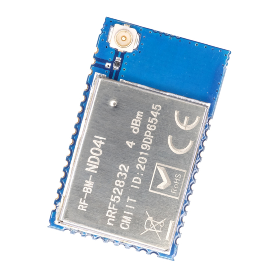
RF-BM-ND04I www.szrfstar.com V1.1 - Sep., 2020 4 Application, Implementation, and Layout 4.1 Module Photos Figure 4. Photos of RF-BM-ND04I 4.2 Recommended PCB Footprint Figure 5. Recommended PCB Footprint of RF-BM-ND04I (mm) Shenzhen RF-star Technology Co., Ltd. Page 12 of 21... -
Page 14: Schematic Diagram
RF-BM-ND04I www.szrfstar.com V1.1 - Sep., 2020 4.3 Schematic Diagram Figure 6. Schematic Diagram of RF-BM-ND04I 4.4 Reference Design Figure 7. Reference Design of RF-BM-ND04I Shenzhen RF-star Technology Co., Ltd. Page 13 of 21... -
Page 15: Antenna
(3) It is best to hollow out the antenna position in the following figure to ensure that the S11 of the module is minimally affected. Figure 8. Recommendation of Antenna Layout Note: The hollow-out position is based on the antenna used. Shenzhen RF-star Technology Co., Ltd. Page 14 of 21... -
Page 16: Ipex Connector
Figure 10. Specification of IPEX Wire 4.5.3 Antenna Output Mode Modification The module has two antenna output modes: IPEX connector output and stamp half-hole antenna output (ANT pin, see pin function table for details). Shenzhen RF-star Technology Co., Ltd. Page 15 of 21... -
Page 17: Basic Operation Of Hardware Design
It is recommended to stay away from the module according to the strength of the interference. If circumstances permit, appropriate isolation and shielding can be done. Shenzhen RF-star Technology Co., Ltd. Page 16 of 21... -
Page 18: Trouble Shooting
3. If the extension wire or feeder wire is of poor quality or too long, the bit error rate will be high. 4.8 Electrostatics Discharge Warnings The module will be damaged for the discharge of static. RF-star suggests that all modules should follow the 3 precautions below: Shenzhen RF-star Technology Co., Ltd. -
Page 19: Soldering And Reflow Condition
T Max. 6 ℃/s Max. 6 ℃/s Time from 25 ℃ to Peak Temperature (t Max. 6 minutes Max. 8 minutes Time of Soldering Zone (t 20±10 s 20±10 s Shenzhen RF-star Technology Co., Ltd. Page 18 of 21... -
Page 20: Optional Packaging
RF-BM-ND04I www.szrfstar.com V1.1 - Sep., 2020 Figure 12. Recommended Reflow for Lead-Free Solder 4.10 Optional Packaging Figure 13. Optional Packaging Mode Note: Default tray packaging. Shenzhen RF-star Technology Co., Ltd. Page 19 of 21... -
Page 21: Revision History
1. The document will be optimized and updated from time to time. Before using this document, please make sure it is the latest version. 2. To obtain the latest document, please download it from the official website: www.szrfstar.com. Shenzhen RF-star Technology Co., Ltd. Page 20 of 21... -
Page 22: Contact Us
RF-BM-ND04I www.szrfstar.com V1.1 - Sep., 2020 6 Contact Us SHENZHEN RF-STAR TECHNOLOGY CO., LTD. Shenzhen HQ: Add.: C601, Skyworth Building, High-tech Park, Nanshan District, Shenzhen, Guangdong, China, 518057 Tel.: 86-755-3695 3756 Chengdu Branch: Add.: B3-03, Building No.1, Incubation Park, High-Tech District, Chengdu, Sichuan, China, 610041 Tel.: 86-28-6577 5970...
Need help?
Do you have a question about the RF-BM-ND04I and is the answer not in the manual?
Questions and answers