
Related Manuals for RF-Star RF-BM-S02A


Summary of Contents for RF-Star RF-BM-S02A
- Page 1 RF-BM-S02A Bluetooth Low Energy Module Version 1.0 Shenzhen RF-star Technology Co., Ltd. May 15 , 2020...
-
Page 2: Ti Cc254X Ble Module List
1. The communication distance is the longest distance obtained by testing the module's maximum transmission power in an open and interference-free environment in sunny weather. 2. Click the picture to buy modules. Shenzhen RF-star Technology Co., Ltd. Page 1 of 25... -
Page 3: Device Overview
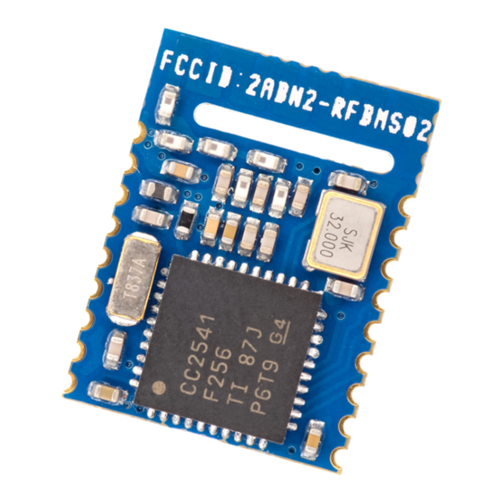
1.1 Description RF-BM-S02A is a Bluetooth Low Energy (BLE) module based on TI CC2541F256, an 8051 core BLE System-on-Chip (SoC). This PCB module integrates a 32 MHz crystal, a 32.768 kHz crystal, an LC balun, an RF matching filter, and a meander line PCB antenna. -
Page 4: Applications
Power Supply 2.0 V ~ 3.6 V Figure 1. Functional Block Diagram of RF-BM-S02A 1.5 Part Number Conventions The part numbers are of the form of RF-BM-S02A where the fields are defined as follows: Company Name Version Number RF-STAR The Second CC2541 Version... -
Page 5: Table Of Contents
4.4 Basic Operation of Hardware Design ...................... 16 4.5 Trouble Shooting .............................. 18 4.5.1 Unsatisfactory Transmission Distance ..................18 4.5.2 Vulnerable Module ..........................18 4.5.3 High Bit Error Rate ..........................18 4.6 Electrostatics Discharge Warnings ......................18 Shenzhen RF-star Technology Co., Ltd. Page 4 of 25... -
Page 6: Table Of Figures
Figure 3. Pin Diagram of RF-BM-S02A ......................8 Figure 4. Photos of RF-BM-S02A ........................15 Figure 5. Recommended PCB Footprint of RF-BM-S02A (mm) ............15 Figure 6. Schematic Diagram of RF-BM-S02A .................... 16 Figure 7. Recommendation of Antenna Layout ................... 17 Figure 8. -
Page 7: Table Of Tables
V1.0 - May, 2020 Table of Tables Table 1. Parameters of RF-BM-S02A ........................ 7 Table 2. Pin Functions of RF-BM-S02A ......................8 Table 3. Recommended Operating Conditions of RF-BM-S02A............10 Table 4. Handling Ratings of RF-BM-ND04 ....................10 Table 5. Table of Receiver RF Parameters ....................10 Table 6. -
Page 8: Module Configuration And Functions
RF-BM-S02A www.szrfstar.com V1.0 - May, 2020 2 Module Configuration and Functions 2.1 Module Parameters Table 1. Parameters of RF-BM-S02A Chipset CC2541F256 Supply Power Voltage 2.0 V ~ 3.6 V, recommended to 3.3 V Frequency 2402 MHz ~ 2480 MHz Transmit Power Programmable: -23.0 dBm ~ 0 dBm... -
Page 9: Module Pin Diagram
RF-BM-S02A www.szrfstar.com V1.0 - May, 2020 2.2 Module Pin Diagram Figure 3. Pin Diagram of RF-BM-S02A 2.3 Pin Functions Table 2. Pin Functions of RF-BM-S02A Name Chip Pin Pin Type Description Ground Power Power supply 2.0 V ~ 3.6 V P2.2... - Page 10 RF-BM-S02A www.szrfstar.com V1.0 - May, 2020 P0.4 P0.3 P0.2 P0.1 Shenzhen RF-star Technology Co., Ltd. Page 9 of 25...
-
Page 11: Specifications
3.3 Receiver RF Parameters Table 5. Table of Receiver RF Parameters When measured on the RF-BM-S02A reference design with T A = 25 ℃, V BAT = 3 V, Fc = 2440 MHz with DC/DC enabled unless otherwise noted. Test Condition Parameters Min. - Page 12 Minimum interferer level < 2 GHz (Wanted signal -67 dBm) Minimum interferer level [2 GHz, 3 GHz] (Wanted signal Out-of-band Blocking Rejection -67 dBm) Minimum interferer level [> 3 GHz] (Wanted signal -67 dBm) Minimum interferer level Intermodulation Shenzhen RF-star Technology Co., Ltd. Page 11 of 25...
- Page 13 -67dBm, 250 bytes payload. BER 0.1% Maximum packet length. Sensitivity better than -67dBm, Symbol Rate Error Tolerance 250 bytes payload. BER 0.1% 250 kbps, GFSK,160 kHz deviation, 0.1% BER Receiver Sensitivity Shenzhen RF-star Technology Co., Ltd. Page 12 of 25...
- Page 14 > 1 GHz Conducted Measurement Note: 1. Difference between center frequency of the received RF signal and local oscillator frequency. 2. Difference between incoming symbol rate and the internally generated symbol rate. Shenzhen RF-star Technology Co., Ltd. Page 13 of 25...
-
Page 15: Transceiver Rf Parameters
3.4 Transceiver RF Parameters Table 6. Table of Transceiver RF Parameters When measured on the RF-BM-S02A reference design with T A = 25 ℃, V BAT = 3 V, Fc = 2440 MHz with DC/DC enabled unless otherwise noted. Parameters Test Condition Min. -
Page 16: Application, Implementation, And Layout
RF-BM-S02A www.szrfstar.com V1.0 - May, 2020 4 Application, Implementation, and Layout 4.1 Module Photos Figure 4. Photos of RF-BM-S02A 4.2 Recommended PCB Footprint Figure 5. Recommended PCB Footprint of RF-BM-S02A (mm) Shenzhen RF-star Technology Co., Ltd. Page 15 of 25... -
Page 17: Schematic Diagram
V1.0 - May, 2020 4.3 Schematic Diagram Figure 6. Schematic Diagram of RF-BM-S02A 4.4 Basic Operation of Hardware Design 1. It is recommended to offer the module with a DC stabilized power supply, a tiny power supply ripple coefficient and the reliable ground. -
Page 18: Figure 7. Recommendation Of Antenna Layout
(3) It is the best to hollow out the red part of the antenna position in the following figure so as to ensure that S11 of the module is minimally affected. Figure 7. Recommendation of Antenna Layout Note: The hollow-out position is based on the antenna used. Shenzhen RF-star Technology Co., Ltd. Page 17 of 25... -
Page 19: Trouble Shooting
3. If the extension wire or feeder wire is of poor quality or too long, the bit error rate will be high. 4.6 Electrostatics Discharge Warnings The module will be damaged for the discharge of static. RF-star suggest that all modules should follow the 3 precautions below: 1. -
Page 20: Soldering And Reflow Condition
Time from 25 ℃ to Peak Temperature (t Max. 6 minutes Max. 8 minutes 20±10 s 20±10 s Time of Soldering Zone (t Figure 8. Recommended Reflow for Lead Free Solder Shenzhen RF-star Technology Co., Ltd. Page 19 of 25... -
Page 21: Optional Packaging
RF-BM-S02A www.szrfstar.com V1.0 - May, 2020 4.8 Optional Packaging Figure 9. Optional Packaging Mode Note: Default tray packaging. Shenzhen RF-star Technology Co., Ltd. Page 20 of 25... -
Page 22: Certification
(2) this device must accept any interference received, including interference that may cause undesired operation. FCC ID: 2ABN2-RFBMS02A Figure 10. FCC Certificate 5.2 CE Verification No.: CCISE170703301V Figure 11. CE Certificate Shenzhen RF-star Technology Co., Ltd. Page 21 of 25... -
Page 23: Rohs
RF-BM-S02A www.szrfstar.com V1.0 - May, 2020 5.3 RoHS Report No.: DTI201801253515 Figure 12. RoHS Certificate 5.4 SRRC SRRC SMIIT ID: 2016DP5705 Figure 13. SRRC Certificate Shenzhen RF-star Technology Co., Ltd. Page 22 of 25... -
Page 24: Reach
RF-BM-S02A www.szrfstar.com V1.0 - May, 2020 5.5 Reach Reach Test Report No.: C150918025001 Figure 14. Reach Certificate Shenzhen RF-star Technology Co., Ltd. Page 23 of 25... -
Page 25: Revision History
1. The document will be optimized and updated from time to time. Before using this document, please make sure it is the latest version. 2. To obtain the latest document, please download it from the official website: www.szrfstar.com. Shenzhen RF-star Technology Co., Ltd. Page 24 of 25... -
Page 26: Contact Us
RF-BM-S02A www.szrfstar.com V1.0 - May, 2020 7 Contact Us SHENZHEN RF-STAR TECHNOLOGY CO., LTD. Shenzhen HQ: Add.: Room 601, Block C, Skyworth Building, High-tech Park, Nanshan District, Shenzhen, Guangdong, China Tel.: 86-755-3695 3756 Chengdu Branch: Add.: No. B3-03, Building No.1, Incubation Park, High-Tech District, Chengdu, Sichuan, China, 610000 Tel.: 86-28-6577 5970...
Need help?
Do you have a question about the RF-BM-S02A and is the answer not in the manual?
Questions and answers