Table of Contents

Related Manuals for NEC Release-it


Summary of Contents for NEC Release-it
- Page 1 User’s Manual Release-it ZigBee -ready Wireless Network Evaluation Board Using the 78K0/KF1+ Microcontroller Hardware Manual Document No. U17586EE1V0UM00 Date Published June 2005 © NEC Electronics Corporation 2005 Printed in Germany...
- Page 2 [MEMO] UM U17586EE1V0UM00...
- Page 3 NEC Electronics does not assume any liability for infringement of patents, copyrights or other intellectual property rights of third parties by or arising from the use of NEC Electronics products listed in this document or any other liability arising from the use of such products. No license, express, implied or otherwise, is granted under any patents, copyrights or other intellectual property rights of NEC Electronics or others.
- Page 4 UM U17586EE1V0UM00...
- Page 5 The information in this document is subject to change without notice. No part of this document may be copied or reproduced in any form or by any means without the prior written consent of NEC Engineering Ltd. and NEC Electronics Corp.
-
Page 6: Table Of Contents
Table of Contents CHAPTER 1 INTRODUCTION ......................7 Features ..............................7 Hardware Specifications .........................8 Interfaces ..............................9 CHAPTER 2 SWITCHES, JUMPERS, AND LEDS ................12 SW4, SW5, SW7, and JP1........................12 2.1.1 Flash Programming Mode........................12 2.1.2 On-chip Debug Mode ........................13 2.1.3 Normal Operation Mode........................13 SW1 .................................14 SW2 and SW3 ............................14 SW6 .................................14 JP2 ................................15... -
Page 7: Features
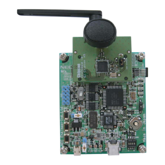
INTRODUCTION CHAPTER 1 RELEASE-IT is an evaluation kit for wireless personal area network using 78K0/KF1+ 8-bit MCU and CC2420 RF transceiver. Features • Hardware is ready to accommodate IEEE 802.15.4/ZigBee compliant wireless personal area network with 8 bit single chip MCU 78K0/KF1+, µPD78F0148HD, and 2.4GHz transceiver CC2420. -
Page 8: Chapter 1 Introduction
CHAPTER 1 INTRODUCTION Hardware Specifications MCU: µPD78F0148HD x 2 Main Clock: 16 MHz Real Time Clock: 32.768 KHz RF Transceiver: Chipcon CC2420, one each on two CC2420EM boards Please refer to www.chipcon.com for further details Antenna: Two Titanis made by Gigaant, www.gigaant.com, one each on the CC2420EM board. Interfaces: USB Mini B Connector between the MCU board and the CC2420EM RF board I/O Expansion of two digital input ports, two digital output ports,... -
Page 9: Interfaces
CHAPTER 1 INTRODUCTION Interfaces I/O Expansion, CN3, HONDA CONNECTORS FFC-10BMEP1 CN3 Name MCU PIN Description N.C. P140 P140/PCL/INTP6 Input to MCU with 4.7KΩ Pull-up P10/SCK10/TXD0 Output from MCU with 4.7KΩ Pull-up P11/SI10/RXD0 Input to MCU with 4.7KΩ Pull-up P12/SO10 Output from MCU with 4.7KΩ Pull-up P24/ANI4 Analog input to MCU with 1MΩ... - Page 10 CHAPTER 1 INTRODUCTION P145/STB0 Output from MCU N.C. SCLK P142/SCKA0 Output from MCU N.C. P144/SOA0 Output from MCU P143/SIA0 Input to MCU Connector to the RF Board (2/2), CN7, SAMTEC TFM-110-02-S-D-A-K-TR CN6 Name MCU Pin Description 3.3V 3.3V N.C. N.C. N.C.
- Page 11 CHAPTER 1 INTRODUCTION Connector to Temp/Humid Sensor, CN8, MAC8 HDB-1-1-4P CN8 Name MCU Pin Description P04/SCK11 Output from MCU 5.0V DATA P05/SSI11/TI001 Input/Output with MCU 1pin Board Edge 4pin CN8 Pin Configuration UM U17586EE1V0UM00...
-
Page 12: Chapter 2 Switches, Jumpers, And Leds
SWITCHES, JUMPERS, AND LEDS CHAPTER 2 SW4, SW5, SW7, and JP1 SW4 and SW5 are a DIP switch to select an operation mode. SW7 is a slide switch to select an operation mode. JP1 is a jumper to select a power source. 2.1.1 Flash Programming Mode Flash EEPROM on the 78K0/KF1+ MCU can be programmed using the attached software “PG-FPL”... -
Page 13: On-Chip Debug Mode
CHAPTER 2 SWITCHES, JUMPERS, AND LEDS 2.1.2 On-chip Debug Mode The following setting activates the On-chip debug functions on the MCU. You can debug your program code in the Flash EEPROM, if your PC is connected to the MCU board via USB. On-chip debug mode Bit 1 Bit 2... -
Page 14: Sw2 And Sw3
CHAPTER 2 SWITCHES, JUMPERS, AND LEDS SW1is a 4 directional switch with center push. If it is directed or pushed, the P7*/KR* input is set to GND. Otherwise the circuit is open. Therefore please set the on-chip pull-up resistors at P7*/KR* during initializing routine of your program code. -
Page 15: Led4
CHAPTER 2 SWITCHES, JUMPERS, AND LEDS JP2 defines the signal level, 5V or 3.3V, of the I/O expansion, CN3. JP2 Settings 5.0V Marked as 5.0V: Pin 1 3.3V Marked as 3.3V: Pin 3 LED4 LED4 is the power indicator. LED1, LED2, and LED3 LED1, LED2, and LED3 are available for applications. -
Page 16: Jumper On The Cc2420Em Board
CHAPTER 2 SWITCHES, JUMPERS, AND LEDS Jumper on the CC2420EM board Please set the jumper on the CC2420EM board as shown in the schematic below. For details of the CC2420EM board, please contact Chipcon AS at www.chipcon.com. UM U17586EE1V0UM00... -
Page 17: Chapter 3 Power Supply
POWER SUPPLY CHAPTER 3 There are two choices to supply power to the board, USB or a 006P battery via CN2. Please refer to 2.1.3 JP1 for the jumper setting. Please replace the battery with a new one, if the voltage level goes down to 6.5V. Below the voltage level of 6.5V, functions of the board are not guaranteed. -
Page 18: Chapter 4 Design Data
DESIGN DATA CHAPTER 4 Parts Layout UM U17586EE1V0UM00... -
Page 19: Connection To Cc2420Em
CHAPTER 4 DESIGN DATA Connection to CC2420EM UM U17586EE1V0UM00... -
Page 20: Circuit Diagram Of The Mcu Board
CHAPTER 4 DESIGN DATA Circuit Diagram of the MCU Board UM U17586EE1V0UM00... - Page 21 CHAPTER 4 DESIGN DATA UM U17586EE1V0UM00...
- Page 22 CHAPTER 4 DESIGN DATA UM U17586EE1V0UM00...
-
Page 23: Dimension Of The Mcu Board
CHAPTER 4 DESIGN DATA Dimension of the MCU Board UM U17586EE1V0UM00... -
Page 24: Pattern Layout Of The Mcu Board
CHAPTER 4 DESIGN DATA Pattern Layout of the MCU Board 4.5.1 Top Side UM U17586EE1V0UM00... -
Page 25: Bottom Side
CHAPTER 4 DESIGN DATA 4.5.2 Bottom Side UM U17586EE1V0UM00... -
Page 26: First Intermediate Layer
CHAPTER 4 DESIGN DATA 4.5.3 First intermediate layer UM U17586EE1V0UM00... -
Page 27: Second Intermediate Layer
CHAPTER 4 DESIGN DATA 4.5.4 Second intermediate layer UM U17586EE1V0UM00... -
Page 28: Third Intermediate Layer
CHAPTER 4 DESIGN DATA 4.5.5 Third intermediate layer UM U17586EE1V0UM00... -
Page 29: Fourth Intermediate Layer
CHAPTER 4 DESIGN DATA 4.5.6 Fourth intermediate layer UM U17586EE1V0UM00... -
Page 30: Bom List
CHAPTER 4 DESIGN DATA BOM List UM U17586EE1V0UM00...
Need help?
Do you have a question about the Release-it and is the answer not in the manual?
Questions and answers