Table of Contents
Advertisement
Quick Links
ISL9237EVAL2Z
Evaluation Board User Guide
Description
The
ISL9237
is a buck-boost Narrow Output Voltage DC (NVDC)
charger utilizing Intersil's advanced R3™ Technology to provide
high light-load efficiency, fast transient response, and
seamless DCM/CCM transitions for a variety of mobile and
industrial applications.
In Charge mode, the ISL9237 takes input power from a wide
range (4V to 20V) of DC power sources (conventional AC/DC
charger adapters, USB PD ports, travel adapters, etc.) and safely
charges battery packs with up to three cells in a series
configuration.
The ISL9237 supports On-the-Go (OTG) function for 2- and
3-cell battery applications. When OTG function is enabled, the
ISL9237 operates in Reverse Buck mode to provide 5V at the
USB port.
The ISL9237 has serial communication via SMBus/I
allows programming of many critical parameters to deliver a
customized solution. These programming parameters include,
but are not limited to: adapter current limit, charger current
limit, system voltage setting, and trickle-charging current limit.
The ISL9237EVAL2Z evaluation board is designed to
demonstrate the performance of the ISL9237. The default
value numbers of the battery in series, the switching
frequency, and the adapter current limit charging function can
be programmed by the resistor from the PROG pin to GND.
Those values also can be set by SMBus.
Related Literature
• For a full list of related documents please visit our website
-
ISL9237
product page
UG075 Rev 3.00
November 4, 2016
2
C that
OPTIONAL
R
s1
VADP
Q1
Q2
CSIN
CSIP
ASGATE
ADP
ACIN
ACOK
PROCHOT#
AMON/BMON
BATGONE
OTGEN/CMIN
FIGURE 1. BLOCK DIAGRAM
USER'S MANUAL
Key Features
• Buck-boost NVDC charger for 1-, 2-, 3-cell Li-ion batteries
• End of Charge (EOC) option
• System power monitor PSYS output, IMVP-8 compliant
• PROCHOT# open-drain output, IMVP-8 compliant
• Allows trickle charging of depleted battery
• Optional ASGATE FET control
• Ideal diode control in Turbo mode
• Reverse buck, boost, and buck-boost operation from battery
• Two-level adapter current limit available
• Battery Ship mode option
• SMBus and auto-increment I
Specifications
• V
= 3.8V to 24V (no dead zone)
IN
• V
= 2.5V to 12.6V
OUT
• MAX I
up to 6A
charge
• f
= 1MHz maximum
SW
Ordering Information
PART NUMBER
ISL9237EVAL2Z
ISL9237 buck-boost charger evaluation board
Q4
L1
Q3
VSYS
CSOP
CSON
ISL9237
BGATE
GND
VBAT
OTGPG/CMOUT
PSYS
UG075
Rev 3.00
November 4, 2016
2
C compatible
DESCRIPTION
VSYS
R
s2
VBAT
Page 1 of 17
Advertisement
Table of Contents

Related Manuals for Renesas ISL9237EVAL2Z


Summary of Contents for Renesas ISL9237EVAL2Z
- Page 1 • MAX I up to 6A charge The ISL9237EVAL2Z evaluation board is designed to • f = 1MHz maximum demonstrate the performance of the ISL9237. The default value numbers of the battery in series, the switching...
-
Page 2: Recommended Equipment
7.8V, connect the battery emulator output to battery leads, J5 and J6. Then, turn on the The ISL9237EVAL2Z provides all circuits that are required to battery emulator; there is no charge and discharge current for evaluate the features of the ISL9237. A majority of the features... - Page 3 ISL9237EVAL2Z FIGURE 2. GUI SNAPSHOT (+) DMM LEAD (+) SUPPLY LEAD (-) DMM LEAD (-) SUPPLY LEAD (+) BATTERY USB PORT LEAD FOR SMBus (-) BATTERY LED 1, 2, 3 BGATE BATGONE LEAD FIGURE 3. EVALUATION BOARD CONNECTION GUIDELINE UG075 Rev 3.00...
- Page 4 ISL9237EVAL2Z Charging Mode Trickle Charging Mode 1. Set the power supply to a constant value between 3.8V and 1. Do steps 1 through 5 in “Charging Mode” without any 24V, then do Steps 1 and 2 in “System Voltage Regulation” on changes.
- Page 5 ISL9237EVAL2Z FIGURE 4. OTG VOLTAGE AND CURRENT SETTING IN GUI FIGURE 5. OTG FUNCTION ENABLE UG075 Rev 3.00 Page 5 of 17 November 4, 2016...
- Page 6 ISL9237EVAL2Z Schematic All NFETs and PFETs are 3x3 size FOR NO ASGATE OPTION 16TQC68MYF 16V, 68uF ESR=50mohm SDA, SCL, ACOK, PROCHOT#, BATGONE, OTGPG/CMOUT, OTGEN all have 3V3 or VDD pull up options For battery connector connection FIGURE 6. ISL9237EVAL2Z BOARD SCHEMATIC...
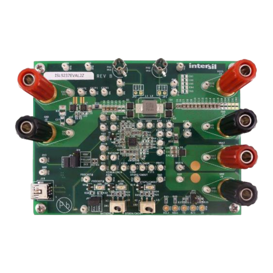
- Page 7 ISL9237EVAL2Z FIGURE 7. TOP OF BOARD FIGURE 8. BOTTOM OF BOARD UG075 Rev 3.00 Page 7 of 17 November 4, 2016...
-
Page 8: Bill Of Materials
ISL9237EVAL2Z Bill of Materials MANUFACTURER PART QTY UNITS REFERENCE DESIGNATOR DESCRIPTION MANUFACTURER ISL9237EVAL1ZREVBPCB SEE LABEL-RENAME BOARD PWB-PCB, ISL9237EVAL1Z, REVB, ROHS IMAGINEERING INC C0603COG500-100KDE CAP, SMD, 0603, 10pF, 50V, 10%, NP0, VENKEL ROHS C0603X7R160102KNE C45, C82 CAP, SMD, 0603, 1000pF, 16V, 10%, X7R,... - Page 9 ISL9237EVAL2Z Bill of Materials (Continued) MANUFACTURER PART QTY UNITS REFERENCE DESIGNATOR DESCRIPTION MANUFACTURER ISL80101IRAJZ IC-ADJ.V, 1A LDO REGULATOR, 10P, DFN, INTERSIL 3x3, ROHS ISL9237HRZ IC-NOTEBOOK BATTERY CHARGER, 32P, INTERSIL QFN, 4x4, ROHS 2N7002-7-F Q8, Q9, Q10 TRANSISTOR, N-CHANNEL, 3LD, SOT-23, DIODES, INC.
-
Page 10: Pcb Layout Guidelines
ISL9237EVAL2Z Bill of Materials (Continued) MANUFACTURER PART QTY UNITS REFERENCE DESIGNATOR DESCRIPTION MANUFACTURER C19, C20, C25, C27, C28, C29, DO NOT POPULATE OR PURCHASE C34, C35, C39, C44, C88-C97 LABEL-DATE CODE AFFIX TO BACK OF PCB LABEL-DATE CODE_LINE 1: YRWK/REV#,... -
Page 11: Pin Number
ISL9237EVAL2Z PCB Layout Guidelines (Continued) PIN NUMBER PIN NAME LAYOUT GUIDELINES PHASE1 Run these two traces in parallel fashion with decent width. Avoid any sensitive analog signal trace from crossing over or getting close. Recommend routing PHASE1 trace to high-side MOSFET source pin instead of general copper. -
Page 12: Board Layout
ISL9237EVAL2Z PCB Layout Guidelines (Continued) PIN NUMBER PIN NAME LAYOUT GUIDELINES VBAT Place the optional RC filter in general proximity of the controller. Run a dedicated trace from the battery positive connection point to the IC. BGATE Use decent width trace from the IC to the BGATE MOSFET gate. Place the capacitor from BGATE to ground close to the MOSFET. - Page 13 ISL9237EVAL2Z Board Layout (Continued) FIGURE 10. INNER LAYER 1 FIGURE 11. INNER LAYER 2 UG075 Rev 3.00 Page 13 of 17 November 4, 2016...
-
Page 14: Typical Performance
ISL9237EVAL2Z Board Layout (Continued) FIGURE 12. BOTTOM LAYER Typical Performance FIGURE 13. BOOST MODE, OUTPUT VOLTAGE LOOP TO ADAPTER FIGURE 14. BOOST MODE, CHARGING CURRENT LOOP TO ADAPTER CURRENT LOOP TRANSITION. V = 5V, CURRENT LOOP TRANSITION. V = 5V, MAXSYSTEMVOLTAGE = 8.496V, V... - Page 15 ISL9237EVAL2Z Typical Performance (Continued) FIGURE 15. BUCK-BOOST MODE, OUTPUT VOLTAGE LOOP TO FIGURE 16. BUCK-BOOST MODE, CHARGING CURRENT LOOP TO ADAPTER CURRENT LOOP TRANSITION. V = 12V, ADAPTER CURRENT LOOP TRANSITION. V = 12V, MAXSYSTEMVOLTAGE = 12.6V, V = 11V, SYSTEM MAXSYSTEMVOLTAGE = 12.6V, V...
- Page 16 ISL9237EVAL2Z Typical Performance (Continued) FIGURE 19. BOOST MODE, OUTPUT VOLTAGE LOOP TO INPUT FIGURE 20. BOOST MODE, CHARGING CURRENT LOOP TO INPUT VOLTAGE LOOP TRANSITION. V = 5V, VOLTAGE LOOP TRANSITION. V = 5V, MAXSYSTEMVOLTAGE = 8.496V, V = 7V, MAXSYSTEMVOLTAGE = 8.496V, V...
-
Page 17: Sales Offices
10. It is the responsibility of the buyer or distributor of Renesas Electronics products, or any other party who distributes, disposes of, or otherwise sells or transfers the product to a third party, to notify such third party in advance of the contents and conditions set forth in this document.
Need help?
Do you have a question about the ISL9237EVAL2Z and is the answer not in the manual?
Questions and answers