Advertisement
Quick Links
QUICK START GUIDE FOR DEMONSTRATION CIRCUIT 630
PIEZOCERAMIC MICROACTUATOR DRIVER WITH BOOST REGULATOR
DESCRIPTION
Demonstration circuit 630 is a g
®
LT
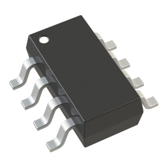
3469ETS8 and can drive an output up to 34V at 25mA
from 5V or 12V supply. An internal Boost converter of the
LT3469 generates a supply voltage up to 36V for the g
amplifier. This regulator switches at 1.5MHz, allowing the
use of a tiny external inductor and capacitor. The 36V output
capability of the switching regulator along with the high
QUICK START PROCEDURE
Demonstration circuit 630 is easy to set up to evaluate the
performance of the LT3469ETS8. Refer to Figure 1 for proper
measurement equipment setup and follow the procedure
below:
NOTE:
When measuring the input or output voltage ripple,
care must be taken to avoid a long ground lead on the
oscilloscope probe. Measure the input or output voltage
ripple by touching the probe tip directly across the V
or V
and GND terminals. See Figure 2 for proper
OUT
scope probe technique.
1.
With power off, connect the input power source V
VIN and GND terminals, connect Vinput to INPUT+ and
GND terminals.
2.
Apply V
=4.75V, Vinput=1V, and Iout=0mA (no load).
IN
Check the boost regulator output Vcc=34.8V±5%, and
input current Iin within the range of 21mA to 35mA.
3.
Apply V
=4.75V, Vinput=1V, and Iout=2mA (2mA load at
IN
V
). Check the boost regulator output Vcc=34.6V±5%,
OUT
amplifier circuit using the
m
IN
to the
IN
supply voltage of the amplifier combine to allow the wide
output voltage range needed to drive a piezoceramic
microactuator.
Design files for this circuit board are available. Call the
m
LTC factory.
LT is a trademark of Linear Technology Corporation
and the input current Iin within the range of 34mA to
50mA.
4.
Apply V
=16V, Vinput=1V, and Iout=0A (no load). Verify
IN
the boost regulator output Vcc=35.2±5%.
5.
Apply V
=5V, Vinput=0.1V, check the amplifier output
IN
V
= within the range of 0.87V to 1.12V.
OUT
6.
Apply V
=5V, Vinput=3V, check the amplifier output
IN
V
= 33V±2%,
OUT
7.
Apply V
=5V and pulsed square wave input that swings
IN
from 0.1V to 2.8V and has period of 300µs to Vinput, and
apply 27nF capacitor load to the output. Verify V
Iout as shown in Figure 3.
LT3469ETS8
and
OUT
1
Advertisement

Summary of Contents for Linear Technology CIRCUIT 630
- Page 1 QUICK START PROCEDURE Demonstration circuit 630 is easy to set up to evaluate the and the input current Iin within the range of 34mA to performance of the LT3469ETS8. Refer to Figure 1 for proper 50mA.
- Page 2 QUICK START GUIDE FOR DEMONSTRATION CIRCUIT 630 PIEZOCERAMIC MICROACTUATOR DRIVER WITH BOOST REGULATOR I OUT V IN Figure 1. Proper Measurement Equipment Setup Figure 2. Measuring Input or Output Ripple...
- Page 3 QUICK START GUIDE FOR DEMONSTRATION CIRCUIT 630 PIEZOCERAMIC MICROACTUATOR DRIVER WITH BOOST REGULATOR Figure 3. Ch2: Vinput. Ch3: Vout. Ch4: Iout, 100mA/Div...
- Page 4 QUICK START GUIDE FOR DEMONSTRATION CIRCUIT 630 PIEZOCERAMIC MICROACTUATOR DRIVER WITH BOOST REGULATOR...
- Page 5 Mouser Electronics Authorized Distributor Click to View Pricing, Inventory, Delivery & Lifecycle Information: Analog Devices Inc. DC630A...


Need help?
Do you have a question about the CIRCUIT 630 and is the answer not in the manual?
Questions and answers