Advertisement
DESCRIPTION
Demonstration circuits 1053A-A through 1053A-
D are high efficiency synchronous boost con-
verters capable of operating with an input volt-
age range from 0.9V to 5.5V. The 2X2 mm DFN
thermally enhanced package with a 1MHz
switching frequency (2MHz for LTC3526-2) and
the 500mA internal switches provide a very tiny
solution. The LTC3526 also features output dis-
connect and the input voltage can be greater or
less than the output voltage.
Table 1. Typical Specifications (25° C)
Input Voltage Range V
1.8V V
OUT
3.3V V
OUT
5V V
OUT
Output Ripple Voltage (burst mode)
Output Ripple Voltage (fixed frequency) V
Efficiency
Efficiency
-
Input
Power
Supply
+
QUICK START GUIDE FOR DEMONSTRATION CIRCUIT
IN
V
IN
V
IN
V
IN
V
IN
IN
V
IN
V
IN
V
A
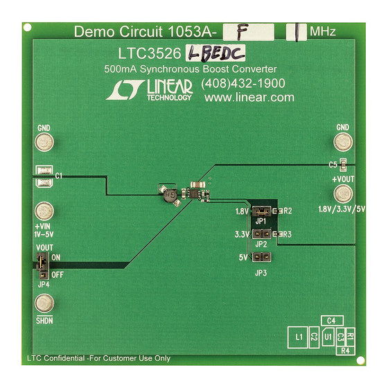
Figure 1. Demonstration Circuit Test Setup
1053A-A through 1053A-D
SYNCHRONOUS BOOST DC/DC CONVERTER
LTC3526/3526B/3526-2/3526B-2
This demonstration circuit allows the user to
quickly evaluate the LTC3526 performance. In-
dividual jumpers are provided for selecting sev-
eral regulated output voltages and a low quies-
cent current shutdown. Terminals on the board
allow easy hookup to an input supply and out-
put load.
Design files for this circuit board are available.
Call the LTC factory.
LTC and Burst Mode are trademarks of Linear Technol-
ogy Corporation
= 1V, I
= 100mA
OUT
= 1.5V, I
= 100mA
OUT
= 1.5V, I
= 100mA
OUT
= 1.2V, V
= 1.8V I
OUT
OUT
= 1.2V, V
= 1.8V I
OUT
OUT
= 1.2V, V
= 1.8V I
OUT
OUT
= 2.5V, V
= 3.3V I
OUT
OUT
1V to 5V
1.8V ± 2.5%
3.3V ± 2.5%
5.0V ± 2.5%
= 1mA
45mV p-p
= 100mA
10mV p-p
= 50mA
85%
= 50mA
92%
Resistive
Load
V
A
1
Advertisement
Table of Contents

Related Manuals for Linear Technology LTC3526


Summary of Contents for Linear Technology LTC3526
- Page 1 500mA internal switches provide a very tiny put load. solution. The LTC3526 also features output dis- Design files for this circuit board are available. connect and the input voltage can be greater or Call the LTC factory.
- Page 2 QUICK START PROCEDURE There is one demonstration circuit board for board. At very low input voltages, voltage all four LTC3526 versions. The boards are drops in the power supply wire, connections identified by the handwritten information on and Ammeter will result in the input voltage at the top of the pc board.
- Page 3 QUICK START GUIDE FOR DEMONSTRATION CIRCUIT 1053A-A THROUGH D SYNCHRONOUS BOOST DC/DC CONVERTER...
Need help?
Do you have a question about the LTC3526 and is the answer not in the manual?
Questions and answers