
Related Manuals for VIA Technologies VAB-5000


Summary of Contents for VIA Technologies VAB-5000
- Page 1 USER MANUAL VIA VAB-5000 Fanless low-power platform for Edge AI applications with MediaTek Genio 700 Octa-Core processor 1.00-30042024...
- Page 2 VIA Technologies, Inc. reserves the right the make changes to the products described in this manual at any time without prior notice.
- Page 3 VIA VAB-5000 User Manual Battery Recycling and Disposal • Only use the appropriate battery specified for this product. • Do not re-use, recharge, or reheat an old battery. • Do not attempt to force open the battery. • Do not discard used batteries with regular trash.
- Page 4 Part Number SoC Frequency Description 10GRB22S900A0 MediaTek Genio 700 VAB-5000 Pico-ITX board with 2.2GHz/2.0GHz MediaTek Genio Octa-Core SoC @ 700 Octa-Core SoC, 16GB eMMC, 4GB LPDDR4X SDRAM, HDMI, 2.2GHz/2.0GHz 40-pin Raspberry Pi-type GPIO, MIPI CSI, 2 USB 3.1, Micro USB 2.0 OTG, Gigabit Ethernet, M.2 slot, Nano SIM card slot, MicroSD card...
-
Page 5: Table Of Contents
VIA VAB-5000 User Manual Table of Contents Product Overview ............................1 Key Features ............................1 Product Specifications ........................... 1 Layout Diagram ............................. 4 Product Dimensions ..........................5 I/O Spacing ............................6 Height Distribution ..........................7 External I/O Pin Descriptions and Functionality ..................... 8 MicroSD Slot ............................ - Page 6 VIA VAB-5000 User Manual Appendix B Optional Accessories ........................26 4G LTE/5G M.2 Wireless Module Kit ....................26 Wi-Fi/Bluetooth Wireless Module ...................... 28 eDP/LVDS and AHD Camera Expansion Board ..................31 MIPI CSI Camera ..........................33 AC-to-DC Power Adapter ........................34 Development Kit ..........................
- Page 7 Figure 38: Connecting an antenna cable to the 4G LTE/5G module ..............28 Figure 39: Remove the M2 screw and nut securing the heat sink plate to the VIA VAB-5000 board ....28 Figure 40: Insert provided M2 screws and bolts to secure Wi-Fi/Bluetooth module on VIA VAB-5000 board .. 29 Figure 41: Tighten the M2 screws and bolts ......................
- Page 8 VIA VAB-5000 User Manual Figure 45: Connecting the cable between the VIA VAB-5000 board and MIPI CSI interface card ...... 33 Figure 46: Connecting the camera module to the MIPI CSI interface card ............33 Figure 47: Debug board jumpers ........................34 Figure 48: Debug board switches ........................
- Page 9 VIA VAB-5000 User Manual List of Tables Table 01: MicroSD card slot pinouts ........................8 Table 02: HDMI port pinouts ..........................8 Table 03: USB 3.1 pinouts ........................... 9 Table 04: Micro USB 2.0 port pinouts ......................... 9 Table 06: Gigabit LAN port LED color definition ....................
-
Page 10: Product Overview
Based on the Pico-ITX form factor, the VIA VAB-5000 board offers a wide variety of I/O and network connectivity options, including a MicroSD card slot, an HDMI port, two USB 3.1 ports, a Micro USB 2.0 OTG port, a 3.5mm headphone jack, a Gigabit Ethernet port, an M.2 slot (to connect the optional 4G LTE or 5G... - Page 11 VIA VAB-5000 User Manual Storage • 16GB eMMC flash memory Graphics • ARM Mali-G57 MC3 High Performance GPU • Graphics engine supporting OpenGL® ES 1.1/2.0/3.2, OpenCL ES 2.2, and Vulkan 1.0/1.1 hardware acceleration • Supports H.265 and H.264 video decoding up to 4K@75fps and video encoding up to 4K@30fps AI Processor •...
- Page 12 VIA VAB-5000 User Manual Power Supply • 1 x 12V DC-in (supports 9V~15V) Operating System • Android 13 • Yocto 4.0 • Debian 12 Operating Temperature • -20°C ~ 60°C Operating Humidity • 0% ~ 95% (relative humidity ; non-condensing) Form Factor •...
-
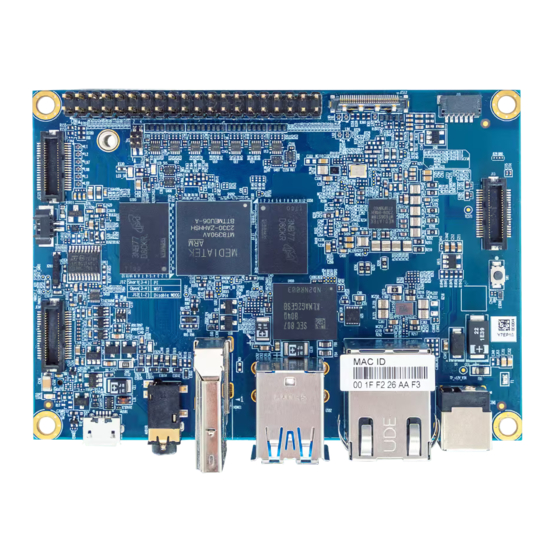
Page 13: Layout Diagram
4-lane MIPI CSI GLAN PMIC MCU Upgrade Header 12V DC-in Wi-Fi/BT B2B Connector Figure 01: VIA VAB-5000 board layout (top I/O view) Micro SD Card Slot Figure 02: VIA VAB-5000 board front I/O view HDMI Gigabit Ethernet 12V DC-in Micro USB 2.0 Audio Jack USB 3.1... -
Page 14: Product Dimensions
Figure 04: VIA VAB-5000 board layout (bottom I/O view) 1.4 Product Dimensions 100mm 94.08mm 2.95mm Figure 05: Dimensions of the VIA VAB-5000 board (top I/O view) 1.6mm 68.95mm Figure 06: External I/O dimensions of the VIA VAB-5000 board (front I/O view) -
Page 15: I/O Spacing
VIA VAB-5000 User Manual 85.33mm 72.68mm 62.77mm 47.23mm 28.29mm 11.34mm Figure 07: External I/O dimensions of the VIA VAB-5000 board (rear I/O view) 1.5 I/O Spacing 3.01mm 10.67mm 2.82mm 7.44mm 5.37mm 5.5mm 3.31mm Figure 08: I/O spacing of the VIA VAB-5000 board (rear I/O view) 15.7mm... -
Page 16: Height Distribution
VIA VAB-5000 User Manual 1.6 Height Distribution 16mm 16mm 16mm 16.4mm Figure 10: Height distribution of the VIA VAB-5000 board (top I/O view) 8.6mm Figure 11: Height distribution of the VIA VAB-5000 board (bottom I/O view) -
Page 17: External I/O Pin Descriptions And Functionality
I/O coastline. 2.1 MicroSD Slot The VIA VAB-5000 board is equipped with a MicroSD Slot on the front coastline, to use for storage of data, pictures, video, audio, documents and so on. The pinouts of the MicroSD slot are shown below. -
Page 18: Usb 3.1 Ports
2.4 Micro USB 2.0 Port The VIA VAB-5000 board is equipped with a Micro USB 2.0 port on the rear coastline. The Micro USB 2.0 port is used for downloading the OS image. The pinouts of the Micro USB 2.0 port are shown below. -
Page 19: Gigabit Lan Port
2.5 Gigabit LAN Port The VIA VAB-5000 board comes with one Gigabit LAN port on the rear coastline. The Gigabit LAN port uses an 8 Position and 8 Contact (8P8C) receptacle connector commonly known as RJ-45, which is fully compliant with the IEEE 802.3 (10BASE-T), 802.3u (100BASE-TX), and 802.3ab (1000BASE-TX) standards. -
Page 20: Dc Jack
VIA VAB-5000 User Manual 2.7 DC Jack The VIA VAB-5000 board comes with a DC Jack located on the rear coastline. The DC Jack is used for suppling 12V-DC power from a compliant adapter. The diagram of the DC Jack is shown below. -
Page 21: On-Board I/O
3.1 40-pin GPIO Header The VIA VAB-5000 board comes with a 40-pin Raspberry Pi-type GPIO header labeled as ‘J6’ which is used for connecting I²C, SPI, UART, PWM, PCM, and 13 I/O expander GPIO devices. The pinouts of the 40-pin GPIO header are shown below. -
Page 22: 4-Lane Mipi Csi Connector
3.2 4-Lane MIPI CSI Connector The VIA VAB-5000 board is equipped with a 30-pin 4-lane MIPI CSI connector labeled 'JCSI2', which can be used for connecting a 2-lane or 4-lane MIPI CSI camera. The pinouts of the MIPI CSI connector are shown below. -
Page 23: Rtc Battery Connector
Table 09: RTC battery connector 'JBAT' pinouts 3.4 Download Button The VIA VAB-5000 board comes with a download button labeled 'SW1'. Connecting the Micro USB OTG to a PC and pressing the 'SW1' button enables the firmware download mode. The diagram of the download button is shown below. -
Page 24: Mcu Upgrade Pin Header
3.5 MCU Upgrade Pin Header The VIA VAB-5000 board is equipped with an MCU upgrade pin header labeled 'J10', which is used for flashing the MCU firmware on the management IC. The pinouts of the MCU upgrade pin header are shown below. -
Page 25: Board-To-Board (B2B) Connectors
VIA VAB-5000 User Manual 3.6 Board-to-Board (B2B) Connectors 3.6.1 Wi-Fi and Bluetooth Connector The VIA VAB-5000 board comes with a 40-pin Wi-Fi 6 and Bluetooth B2B connector labeled 'J13', for connecting the optional dual-band Wi-Fi 6 and Bluetooth 5.2 module. The pinouts of the Wi-Fi and Bluetooth B2B connector are shown below. -
Page 26: Csi-To-Ahd Connector
VIA VAB-5000 User Manual 3.6.2 CSI-to-AHD Connector The VIA VAB-5000 board comes with a 40-pin CSI-to-AHD B2B connector labeled 'JCSI1', for connecting the optional eDP + AHD camera or LVDS + AHD camera expansion board. The pinouts of the CSI-to-AHD B2B connector are shown below. -
Page 27: Edp Connector
VIA VAB-5000 User Manual 3.6.3 eDP Connector The VIA VAB-5000 board comes with a 40-pin eDP B2B connector labeled 'JEDP', for connecting the optional eDP + AHD camera or LVDS + AHD camera expansion board. The pinouts of the eDP B2B connector are shown below. -
Page 28: Slot
VIA VAB-5000 User Manual 3.7 M.2 Slot The VIA VAB-5000 board is equipped with an M.2 format 3042 Key B slot, labeled 'MB2', for connecting the optional 4G LTE or 5G M.2 module. The pinouts of the M.2 slot are shown below. -
Page 29: Nano Sim Card Slot
3.8 Nano SIM Card Slot The VIA VAB-5000 board comes with a Nano SIM card slot labeled 'SIM1'. It supports 4G LTE and 5G SIM cards. SIM card usage requires that the optional 4G LTE or 5G module is installed in the M.2 slot, otherwise the Nano SIM card slot will be disabled. -
Page 30: Onboard Jumpers
1 and pin 2 or pin 2 and 3 to Short it. Some jumpers' sizes are small or mounted on a crowded location on the VIA VAB-5000 board that makes it difficult to access. -
Page 31: Watchdog/Pcm Bus Select Jumper
3.10.2 Auto Power ON Header The VIA VAB-5000 board comes with a 4-pin auto power ON jumper labeled as 'J14'. The jumper is used to enable or disable the auto power ON function on the VIA VAB-5000 board. The auto power ON jumper settings are shown below. -
Page 32: Software And Technical Support
VIA VAB-5000 User Manual 4. Software and Technical Support 4.1 Android, Yocto and Debian Support The VIA VAB-5000 features complete software evaluation images for Android 13, Yocto 4.0, and Debian 12 operating systems. 4.2 Technical Support and Assistance • For utilities downloads and the latest documentation and information about the VIA VAB-5000, please visit our website at https://www.viatech.com/en/edge/vab-5000/. -
Page 33: Appendix A Recommended Mating/Unmating Jig
VIA VAB-5000 User Manual Appendix A Recommended Mating/ Unmating Jig This chapter describes how to use the recommended mating/unmating jig for fixing the: • MHF - I mating/unmating jig for fixing the 4G LTE/5G antennas' plug connectors on the micro- miniature RF antenna connectors (I-PEX) located on the top surface of the optional 4G LTE/5G Wireless Module. -
Page 34: Mating Method Of Plug Connector
VIA VAB-5000 User Manual MHF4 90435-001 Figure 34: MHF - 4 mating/unmating jig dimensions A.2 Mating Method of Plug Connector Using the jig, align the plug connector with the micro-miniature RF antenna connector (I-PEX). Then push down gently until the plug connector is fully connected. The recommended force is 30N (maximum). -
Page 35: Appendix B Optional Accessories
Step 1 Follow the instructions below to install an activated 4G LTE or 5G Nano SIM card: 1. Firmly push back to unlock the Nano SIM card slot located on the bottom surface of the VIA VAB-5000 board. 2. Pull up the slot and slide in the Nano SIM card, ensuring that the correct end goes in. -
Page 36: Figure 37: Installing The 4G Lte/5G Module On The Via Vab-5000 Board
If the 5G module will be installed, skip this step. Step 3 Align the 4G LTE/5G module's notch with the notch of the M.2 B-key slot located on the VIA VAB-5000 board's bottom surface and insert the 4G LTE/5G module at a 30° angle. -
Page 37: Wi-Fi/Bluetooth Wireless Module
Wi-Fi and Bluetooth module: Step 1 Remove the M2*6mm screw and M2 nut securing the heat sink plate to the VIA VAB-5000 board. Figure 39: Remove the M2 screw and nut securing the heat sink plate to the VIA VAB-5000 board... -
Page 38: Figure 40: Insert Provided M2 Screws And Bolts To Secure Wi-Fi/Bluetooth Module On Via Vab-5000 Board
1. Insert the provided M2*4mm screw into the top left corner screw hole of the Wi-Fi/Bluetooth module. 2. Place M2*10mm bolts (provided with the VIA VAB-5000 board) under the bottom left and bottom right corner screw holes of the VIA VAB-5000 board, then insert the provided M2*15mm screws into the corresponding standoff screw holes of the Wi-Fi/Bluetooth module. -
Page 39: Figure 41: Tighten The M2 Screws And Bolts
VIA VAB-5000 User Manual Step 3 Tighten all the screws with a Phillips #1 screwdriver. Figure 41: Tighten the M2 screws and bolts Step 4 Affix the provided antennas on the micro-RF (IPEX) connectors labeled 'W6ANT_WIFI1', 'W6ANT_WIFI2', and 'W6ANT_BT1' on the Wi-Fi and Bluetooth module. -
Page 40: Edp/Lvds And Ahd Camera Expansion Board
Step 1 Insert the expansion board's eDP/LVDS and AHD camera B2B connectors into the VIA VAB-5000 board's eDP and CSI-to-AHD B2B connectors, then secure the expansion board on the VIA VAB-5000 board as follows: 1. -
Page 41: Figure 44: Tighten The M2 Screws And Bolts
VIA VAB-5000 User Manual Step 2 Tighten all the screws with a Phillips #1 screwdriver. Figure 44: Tighten the M2 screws and bolts... -
Page 42: Mipi Csi Camera
Step 1 Connect one end of the cable to the MIPI CSI connector labeled 'JCSI2' on the VIA VAB-5000 board, and connect the other end of the cable to the MIPI CSI connector labeled 'JCSI1' on the MIPI CSI interface card. -
Page 43: Ac-To-Dc Power Adapter
The optional development kit includes a USB to UART debug board and a 3-pin cable to connect the VIA VAB- 5000 device to a host PC for debugging. Note: Make sure that the VIA VAB-5000 is powered OFF before setting the debug board jumpers and switch, and installing the development kit. B.6.1 Debug Board Jumper and Switch Settings... -
Page 44: Figure 48: Debug Board Switches
VIA VAB-5000 User Manual The UART routing switch set 'SW1' has two switches labeled '1' and '2' that can be toggled ON/OFF. The UART voltage switch 'SW2' can be toggled 1.8V/3.3V. Figure 48: Debug board switches To set the USB to UART route and UART voltage, set the debug board jumpers and switches as described below. -
Page 45: Installation
Figure 50: Connecting the 3-pin cable between the VIA VAB-5000 board and host PC Step 4 Power ON the VIA VAB-5000 board. While debugging, the red RX LED on the debug board flashes when a signal is received, and the green TX LED flashes when a signal is transmitted. - Page 46 Taiwan Headquarters Japan China 1F, 531 Zhong-zheng Road, 940 Mission Court 3-15-7 Ebisu MT Bldg. 6F, Tsinghua Science Park Bldg. 7 Xindian Dist., New Taipei City 231 Fremont, CA 94539, Higashi, Shibuya-ku No. 1 Zongguancun East Road, Taiwan Tokyo 150-0011 Haidian Dist., Beijing, 100084 Japan China...
Need help?
Do you have a question about the VAB-5000 and is the answer not in the manual?
Questions and answers