Table of Contents
Advertisement
TABLE OF CONTENTS
1 Safety Precautions----------------------------------------------- 3
1.1. General Guidelines---------------------------------------- 3
1.2. Caution for AC Cord (For EB only)-------------------- 4
1.3. Before Repair and Adjustment ------------------------- 4
1.4. Protection Circuitry ---------------------------------------- 4
1.5. Caution For Fuse Replacement------------------------ 4
1.6. Safety Part Information----------------------------------- 5
2 Warning -------------------------------------------------------------- 6
to Electrostatically Sensitive (ES) Devices---------- 6
2.2. Precaution of Laser Diode------------------------------- 7
2.4. Handling Precaution for Traverse Unit --------------- 8
3 Service Navigation ----------------------------------------------- 9
3.1. Service Information --------------------------------------- 9
3.2. Software Update through USB ------------------------- 9
4 Specifications ----------------------------------------------------10
5 Location of Controls and Components ------------------11
Model No.
Product Color: (K)...Black Type (For HC395EG,
PAGE
Operations ------------------------------------------------- 11
6 Service Mode ----------------------------------------------------- 12
6.1. Self Diagnostic Table------------------------------------ 12
6.2. Self Diagnostic Function Error Code ---------------- 13
7 Troubleshooting Guide --------------------------------------- 15
8 Disassembly and Assembly Instructions--------------- 17
8.1. Service Fixture & Tools --------------------------------- 17
8.2. Disassembly flow chart --------------------------------- 18
8.3. Types of Screws------------------------------------------ 20
8.4. Main Parts Location Diagram ------------------------- 20
8.5. Disassembly of Base Stand Unit --------------------- 21
8.7. Disassembly of Door Unit ------------------------------ 22
8.8. Disassembly of Door Base ---------------------------- 22
8.9. Disassembly of Front Panel Block ------------------- 23
8.10. Disassembly of Bridge P.C.B.------------------------- 24
8.11. Disassembly of Motor P.C.B.-------------------------- 25
© Panasonic Corporation 2016. All rights reserved.
Unauthorized copying and distribution is a violation of
law.
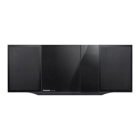
Compact Stereo System
SC-HC395EG
SC-HC397EB
SC-HC397EG
HC397EG)
(S)...Silver Type
(W)...White Type (For HC395EG,
HC397EG)
PSG1602001CE
PAGE
Advertisement
Table of Contents

Related Manuals for Panasonic SC-HC395EG


Summary of Contents for Panasonic SC-HC395EG
-
Page 1: Table Of Contents
8.9. Disassembly of Front Panel Block ------------------- 23 4 Specifications ----------------------------------------------------10 8.10. Disassembly of Bridge P.C.B.------------------------- 24 5 Location of Controls and Components ------------------11 8.11. Disassembly of Motor P.C.B.-------------------------- 25 © Panasonic Corporation 2016. All rights reserved. Unauthorized copying and distribution is a violation of law. - Page 2 8.12. Disassembly of Gear Block & Arm Spring 14.1. Voltage Measurement ---------------------------------- 81 (Top) -------------------------------------------------------- 25 15 Exploded View and Replacement Parts List----------- 85 8.13. Disassembly of Arm Spring, Gear Assembly & 15.1. Exploded View and Mechanical replacement Arm Assembly ------------------------------------------- 26 Parts List --------------------------------------------------- 85 8.14.
-
Page 3: Safety Precautions
1 Safety Precautions 1.1. General Guidelines 1. IMPORTANT SAFETY NOTICE There are special components used in this equipment which are important for safety. These parts are marked by in the Schematic Diagrams, Circuit Board Layout, Exploded Views and Replacement Parts List. It is essential that these critical parts should be replaced with manufacturer’s specified parts to prevent X-RADIATION, shock, fire, or other hazards. -
Page 4: Caution For Ac Cord (For Eb Only)
1.2. Caution for AC Cord (For EB only) 1.3. Before Repair and Adjustment Disconnect AC power, discharge unit AC Capacitors (C1702, C1710, C1725, C1727 and C1728) through a 10W, 1W resistor to ground. Caution : DO NOT SHORT-CIRCUIT DIRECTLY (with a screwdriver blade, for instance), as this may destroy solid state devices. After repairs are completed, restore power gradually using a variac, to avoid overcurrent. -
Page 5: Safety Part Information
1.6. Safety Part Information Safety Parts List: There are special components used in this equipment which are important for safety. These parts are marked by in the Schematic Diagrams, Exploded View & Replacement Parts List. It is essential that these critical parts should be replaced with manufacturer’s specified parts to prevent shock, fire or other hazards. -
Page 6: Warning
2 Warning 2.1. Prevention of Electrostatic Discharge (ESD) to Electrostatically Sensi- tive (ES) Devices Some semiconductor (solid state) devices can be damaged easily by static electricity. Such components commonly are called Elec- trostatically Sensitive (ES) Devices. The following techniques should be used to help reduce the incidence of component damage caused by electrostatic discharge (ESD). -
Page 7: Precaution Of Laser Diode
2.2. Precaution of Laser Diode CAUTION! THIS PRODUCT UTILIZES A LASER. USE OF CONTROLS OR ADJUSTMENTS OR PERFORMANCE OF PROCEDURES OTHER THAN THOSE SPECIFIED HEREIN MAY RESULT IN HAZARDOUS RADIATION EXPOSURE. Caution: This product utilizes a laser diode with the unit turned "on", invisible laser radiation is emitted from the pickup lens. Wavelength: 790 nm (CD) Maximum output radiation power from pickup: 100 μW/VDE Laser radiation from the pickup unit is safety level, but be sure the followings:... -
Page 8: Handling Precaution For Traverse Unit
2.4. Handling Precaution for Traverse Unit The laser diode in the optical pickup unit may break down due to static electricity of clothes or human body. Special care must be taken avoid caution to electrostatic breakdown when servicing and handling the laser diode in the Traverse Unit. Cautions to Be Taken in Handling the Optical Pickup Unit 2.4.1. -
Page 9: Service Navigation
3 Service Navigation 3.1. Service Information This service manual contains technical information which will allow service personnel’s to understand and service this model. Please place orders using the parts list and not the drawing reference numbers. If the circuit is changed or modified, this information will be followed by supplement service manual to be filed with original service manual. -
Page 10: Specifications
4 Specifications • Specifications are subject to change without notice. • Mass and dimensions are approximate. General • Total harmonic distortion is measured by a digital spectrum ana- Power consumption 26 W lyzer. Power consumption in standby Approx. 0.2 W *1: “BLUETOOTH STANDBY”... -
Page 11: Location Of Controls And Components
5 Location of Controls and Components 5.1. Main Unit & Remote Control Key Button Operations... -
Page 12: Service Mode
6 Service Mode This unit is equipped with features of self diagnostic & doctor mode setting for checking the functions & reliability. 6.1. Self Diagnostic Table Item FL display Key operation Mode name Description Step 1 : Select CD mode Self Diagnostic Mode To enter into self diagnostic (Ensure no disc is inserted). -
Page 13: Self Diagnostic Function Error Code
6.2. Self Diagnostic Function Error Code 6.2.1. CD Mechanism Error Code Table Error Code Diagnostic Contents Description of error of error Automatic FL Display Remarks During normal operation, if CD H15 CD Open Abnormal Press [ ] on main unit for “POS_SW_R (OPEN_SW)”... -
Page 15: Troubleshooting Guide
7 Troubleshooting Guide Power do not turn on Power on by remote control Main set power ON Check the connection of FFC connector from FL PCB to Main PCB Check the 14P of [FL]-[Main] FFC connector CN900 to CN6007. (For HC395/HC397) (The FL display "HELLO"... -
Page 17: Disassembly And Assembly Instructions
8 Disassembly and Assembly Instructions Caution Note: • This section describes the disassembly and/or assembly procedures for all major printed circuit boards & main compo- nents for the unit. (You may refer to the section of “Main components and P.C.B Locations” as described in this service manual) •... -
Page 18: Disassembly Flow Chart
8.2. Disassembly flow chart The following chart is the procedure for disassembling the casing and inside parts for internal inspection when carrying out the ser- vicing. To assemble the unit, reverse the steps shown in the chart below. For HC395... - Page 19 For HC397...
-
Page 20: Types Of Screws
8.3. Types of Screws 8.4. Main Parts Location Diagram... -
Page 21: Disassembly Of Base Stand Unit
8.5. Disassembly of Base Stand 8.6. Disassembly of Front Orna- Unit ment Unit (L) & (R) Step 1 : Remove screw. Step 2 : Remove Base Stand Unit. Note : The disassembling procedure for Front Ornament Unit (L) will be described here only. For Front Ornament Unit (R) please refer to the same proce- dure described here. -
Page 22: Disassembly Of Door Unit
8.7. Disassembly of Door Unit 8.8. Disassembly of Door Base • Refer to “Disassembly of Front Ornament Unit (L)” • Refer to “Disassembly of Front Ornament Unit (L)” • Refer to “Disassembly of Door Unit” Step 1 : Lift up Door Unit. Step 2 : Slide Door Unit to open it. -
Page 23: Disassembly Of Front Panel Block
8.9. Disassembly of Front Panel Step 4 : Remove 2 screws. Step 5 : Slide Door Unit to close it. Block Step 6 : Release catches on Front Panel Block. • Refer to “Disassembly of Front Ornament Unit (L) & (R)” Step 7 : Slightly lift up Front Panel Block. -
Page 24: Disassembly Of Bridge P.c.b
Step 8 : Detach 14P FFC at connector (CN941) on Bridge 8.10. Disassembly of Bridge P.C.B. P.C.B.. • Refer to “Disassembly of Front Ornament Unit (L) & (R)” Step 9 : Remove Front Panel Block. • Refer to “Disassembly of Front Panel Block” Step 1 : Remove screw. -
Page 25: Disassembly Of Motor P.c.b
8.11. Disassembly of Motor P.C.B. 8.12. Disassembly of Gear Block & Arm Spring (Top) • Refer to “Disassembly of Front Ornament Unit (L) & (R)” • Refer to “Disassembly of Front Panel Block” • Refer to “Disassembly of Front Ornament Unit (L) & (R)” •... -
Page 26: Arm Assembly
Step 4 : Release Arm Spring (Top) from ribs. 8.13. Disassembly of Arm Spring, Step 5 : Remove Arm Spring (Top). Gear Assembly & Arm Assem- • Refer to “Disassembly of Front Ornament Unit (L) & (R)” • Refer to “Disassembly of Door Unit” •... - Page 27 Step 3 : Remove screw. Caution : During assembling, position & align Gear B with the indicated arrow on Gear Assembly. Step 4 : Release catches. Step 5 : Remove Gear Cover. Step 6 : Remove Arm Assembly & Gear Assembly.
-
Page 28: Replacement Of Gear Assembly
8.14. Replacement of Gear Assem- 8.14.2. Disassembly of Gear C • Refer to “Disassembly of Belt, Pulley Gear, Gear B & Gear A” • Refer to “Disassembly of Front Ornament Unit (L) & (R)” • Refer to “Disassembly of Door Unit” Step 1 : Remove Gear C. -
Page 29: Replacement Of Arm Assembly
8.14.3. Disassembly of Motor Assembly 8.15. Replacement of Arm Assembly • Refer to “Refer to (Step 1) of item 8.14.1.” • Refer to “Disassembly of Front Ornament Unit (L) & (R)” • Refer to “Disassembly of Door Unit” Step 1 : Desolder pins on solder side of Motor P.C.B.. •... - Page 30 Step 3 : Remove Drive Gear, Door Holder & Gear Shaft. 8.15.2. Disassembly of Arm Bracket Metal, Door Arm Top & Door Arm Bottom • Refer to “Disassembly of Drive Gear, Door Holder & Gear Shaft” Step 1 : Remove 2 screws. Caution : During assembling, ensure Door Holder Rib is parallel into the Gear Shaft.
-
Page 31: Disassembly Of Cam Rail Top & Door Slider Top
8.16. Disassembly of Cam Rail Top & Step 4 : Remove Door Slider Top. Door Slider Top • Refer to “Disassembly of Front Ornament Unit (L) & (R)” • Refer to “Disassembly of Door Unit” • Refer to “Disassembly of Front Panel Block” Step 1 : Remove 2 screws. -
Page 32: Disassembly Of Cam Rail Bottom & Door Slider Bottom
8.17. Disassembly of Cam Rail Bot- Step 3 : Remove Door Slider Bottom. tom & Door Slider Bottom • Refer to “Disassembly of Front Ornament Unit (L) & (R)” • Refer to “Disassembly of Door Unit” • Refer to “Disassembly of Front Panel Block” •... -
Page 33: Disassembly Of Nfc P.c.b
8.18. Disassembly of NFC P.C.B. Step 3 : Lift up NFC P.C.B.. Step 4 : Detach 2P wire at connector (CN7001) on NFC P.C.B.. • Refer to “Disassembly of Front Ornament Unit (L) & (R)” Step 5 : Remove NFC P.C.B.. •... -
Page 34: Disassembly Of Smps Unit
8.19. Disassembly of SMPS Unit 8.20. Disassembly of SMPS P.C.B. • Refer to “Disassembly of Front Ornament Unit (L) & (R)” • Refer to “Disassembly of SMPS Unit” • Refer to “Disassembly of Front Panel Block” Step 1 : Remove screw. Step 1 : Remove 5 screws. - Page 35 Step 5 : Press to release catches using a screwdriver and gen- Step 6 : Gently push up SMPS Shield Unit to release catches tly push up SMPS Shield Unit. and remove it. Caution : During assembling, ensure SMPS Shield Unit is Caution : During assembling, ensure SMPS Shield properly catched to SMPS bracket as shown.
-
Page 36: Disassembly Of Fl P.c.b. & Button Ornament Unit
8.21. Disassembly of FL P.C.B. & 8.22. Disassembly of Button P.C.B. Button Ornament Unit • Refer to “Disassembly of Front Ornament Unit (L) & (R)” • Refer to “Disassembly of Front Panel Block” • Refer to “Disassembly of Front Ornament Unit (L) & (R)” •... -
Page 37: Disassembly Of Cd Mechanism
8.23. Disassembly of CD Mechanism Step 3 : Detach 24P FFC at connector (P5003) on Main P.C.B.. Step 4 : Remove CD Mechanism. • Refer to “Disassembly of Front Ornament Unit (L) & (R)” • Refer to “Disassembly of Front Panel Block” Step 1 : Remove 2 screws. -
Page 38: Disassembly Of Cd Interface P.c.b
8.24. Disassembly of CD Interface Step 2 : Lift up Mecha Chassis & remove Floating Springs. Caution : Keep the Floating Springs and place them back P.C.B. during assembling. • Refer to “Disassembly of CD Mechanism” Step 1 : Release catches and push down fixed pins as arrow shown. -
Page 39: Disassembly Of Dab Module And Dab Adapter P.c.b. (For Hc397)
Step 7 : Attach short pin to 24P FFC of Traverse Unit. 8.25. Disassembly of DAB Module Step 8 : Remove CD Interface P.C.B.. and DAB Adapter P.C.B. (For HC397) • Refer to “Disassembly of Front Ornament Unit (L) & (R)” •... -
Page 40: Disassembly Of Main P.c.b. (For Hc395)
Step 5 : Lift up to remove DAB Unit. 8.26. Disassembly of Main P.C.B. (For HC395) • Refer to “Disassembly of Front Ornament Unit (L) & (R)” • Refer to “Disassembly of Front Panel Block” • Refer to “Disassembly of SMPS Unit” •... -
Page 41: Disassembly Of Main P.c.b. (For Hc397)
Step 4 : Detach 14P FFC at connector (CN6007) on Main 8.27. Disassembly of Main P.C.B. P.C.B.. (For HC397) Step 5 : Detach 2P wire at connector (CN400) on Main P.C.B.. Step 6 : Detach 2P wire at connector (CN401) on Main P.C.B.. •... -
Page 42: Disassembly Of Front Speaker (Sp1)
8.28. Disassembly of Front Speaker Step 5 : Desolder speaker wire at the terminals on Front Speaker (SP1). (SP1) • Refer to “Disassembly of Front Ornament Unit (L) & (R)” • Refer to “Disassembly of Front Panel Block” • Refer to “Disassembly of NFC P.C.B.” •... -
Page 43: Disassembly Of Front Speaker (Sp2)
8.29. Disassembly of Front Speaker Step 3 : Remove 3 screws. Step 4 : Remove Speaker Cabinet Unit (R) Block. (SP2) • Refer to “Disassembly of Front Ornament Unit (L) & (R)” • Refer to “Disassembly of Front Panel Block” •... -
Page 44: Disassembly Of Passive Radiator Unit (Sp3)
Step 6 : Remove 4 screws. 8.30. Disassembly of Passive Radia- Step 7 : Remove Front Speaker (SP2). tor Unit (SP3) • Refer to “Disassembly of Front Ornament Unit (L) & (R)” • Refer to “Disassembly of Front Panel Block” •... -
Page 45: Disassembly Of Passive Radiator Unit (Sp4)
8.31. Disassembly of Passive Radia- 8.32. Disassembly of Jack Lid tor Unit (SP4) • Refer to “Disassembly of Front Ornament Unit (L) & (R)” • Refer to “Disassembly of Front Panel Block” • Refer to “Disassembly of Front Ornament Unit (L) & (R)” •... - Page 46 Step 3 : Lift up to remove Jack Lid in the direction as shown.
-
Page 47: Service Position
9 Service Position Note: For description of the disassembly procedures, see the Section 8 9.1. Checking of SMPS P.C.B. Step 9 : Place a Support Block to support Front Panel Block as shown. Step 10 : Connect 14P FFC at connector (CN941) on Bridge Step 1 : Remove Front Ornament Unit (L) &... -
Page 48: Checking Of Fl P.c.b
Step 13 : Check SMPS P.C.B. according to the diagram shown. 9.2. Checking of FL P.C.B. Step 1 : Remove Front Ornament Unit (L) & (R). Step 2 : Remove Front Panel Block. Step 3 : Remove NFC P.C.B.. Step 4 : Remove 2 screws. Step 5 : Detach 14P FFC at connector (CN900) on Button P.C.B.. - Page 49 Step 9 : Release catches. Step 13 : Place FL P.C.B. on the Insulating Material. Step 10 : Remove Bridge P.C.B.. Step 14 : Connect 14P FFC at connector (CN900) on FL P.C.B.. Step 15 : Connect 2P wire at connector (CN7001) on NFC P.C.B..
-
Page 50: Checking Of Cd Interface P.c.b
9.3. Checking of CD Interface P.C.B. Step 8 : Place a Support Block to support Front Panel Block as shown. Note : Insert CD before Checking CD Interface P.C.B. Step 9 : Connect 14P FFC at connector (CN941) on Bridge P.C.B.. -
Page 51: Checking Of Main P.c.b
Step 12 : Check CD Interface P.C.B. according to the diagram 9.4. Checking of Main P.C.B. shown. Step 1 : Remove Front Ornament Unit (L) & (R). Step 2 : Remove Front Panel Block. Step 3 : Remove NFC P.C.B.. Step 4 : Remove SMPS Unit. - Page 52 Step 12 : Place Bottom Ornament Unit & NFC P.C.B. on Insu- Step 15 : Place SMPS Unit as shown. lating Material. Step 16 : Connect 7P extension cable (REX1538) from Step 13 : Connect 14P FFC at connector (CN6007) on Main CN1100 on Main P.C.B.
- Page 53 Step 19 : Remove screw. Step 23 : Place Front Panel Block as shown. Step 20 : Release 5P wire from the slots. Step 24 : Connect 14P FFC at connector (CN941) on Bridge P.C.B.. Step 21 : Release catches. Step 22 : Remove Bridge P.C.B..
-
Page 55: Block Diagram
10 Block Diagram 10.1. SYSTEM CONTROL (1/2) BLOCK DIAGRAM... -
Page 56: System Control (2/2) Block Diagram
10.2. SYSTEM CONTROL (2/2) BLOCK DIAGRAM... -
Page 57: Audio Block Diagram
10.3. AUDIO BLOCK DIAGRAM... -
Page 58: Power Supply (1/2) Block Diagram
+5V VOLTAGE +5V VOLTAGE BLOCK (2/2) REGULATOR REGULATOR PW BT5V PW BT5V VOUT VOUT M VDET M VDET SYSTEM CONTROL Q404 SWITCH PW DAMP19V PW DAMP19V QR400 SWITCH FROM SMPS CUT SMPS CUT SYSTEM CONTROL SC-HC395EG,SC-HC397EB/EG POWER SUPPLY (1/2) BLOCK DIAGRAM... -
Page 59: Power Supply (2/2) Block Diagram
1.2V 3.3V VOUT 3 +3.3V VOLTAGE REGULATOR 5.7V 3.3V D3.3V Z950 D3.3V 3.3V 3.3V PW D5R7V DAB 5.7V CN6000 CN950 5.7V 5.7V VOUT 1 DAB ADAPTER P.C.B. DAB MODULE TO POWER SUPPLY BLOCK (1/2) SC-HC395EG,SC-HC397EB/EG POWER SUPPLY (2/2) BLOCK DIAGRAM... -
Page 60: Wiring Connection Diagram
P6801 CN7001* NFC P.C.B. NOTE: " * " REF IS FOR INDICATION ONLY. SC-HC395EG, SC-HC397EB/EG (NFC PCB and IC8004) and (NFC PCB and MAIN PCB) are supplied as a kit. For the details, refer to "Service Navigation". WIRING CONNECTION DIAGRAM... -
Page 61: Schematic Diagram
12 Schematic Diagram 12.1. Schematic Diagram Notes • Voltage and signal line (All schematic diagrams may be modified at any time with : +B Signal Line the development of new technology) : -B Signal Line Notes: : CD Signal Line S641: OPEN switch. -
Page 63: Cd Interface Circuit
OPTICAL PICKUP UNIT R5025 J0JYB0000013 VREF VCC(5V) R5026 CD-LD MD/LPD R5021 R5019 R5020 C5021 R5022 DVD-LD 100K Q5001 GND-LD B1ADCF000001 LASER DRIVE C5020 C5023 C8018 R5023 0.01 NOTE: “ * ” REF IS FOR INDICATION ONLY SC-HC395EG, SC-HC397EB/EG CD INTERFACE CIRCUIT... -
Page 64: Main (Micon) Circuit (1/2)
DC_DET_AMP R8022 100K TRST POSITION(CTR) R8006 100K D8000 USB_OVER_CUR B0ADDH000009 POSITION(LEFT) R8005 100K DVDDIO CHARGE_EN LOADING TO MAIN (MICON) CIRCUIT (2/2) Q8000 B1GBCFNN0038 SC-HC395EG, SC-HC397EB/EG RX8007 SWITCH J0JAD0000007 NOTE: “ * ” REF IS FOR INDICATION ONLY MAIN (MICON) CIRCUIT... -
Page 65: Main (Micon) Circuit (2/2)
R216...HC397 B1HFCDE00002 PW_iPod5V PCONT R8053 330K KEY1 R111...HC397 R214...HC395 C5054 CD: MAIN (CD): SCHEMATIC DIAGRAM - 5 DVSSQ US: MAIN (USB): SCHEMATIC DIAGRAM - 6 TU: MAIN (TUNER): SCHEMATIC DIAGRAM - 8 PCONT3 R8003 2.2K SC-HC395EG, SC-HC397EB/EG MAIN (MICON) CIRCUIT... -
Page 66: Main (Supply) Circuit
MI: MAIN (MICON): SCHEMATIC DIAGRAM - 2 ~ 3 CD: MAIN (CD): SCHEMATIC DIAGRAM - 5 US: MAIN (USB): SCHEMATIC DIAGRAM - 6 DA: MAIN (DAMP): SCHEMATIC DIAGRAM - 7 NOTE: “ * ” REF IS FOR INDICATION ONLY iPod_GND SC-HC395EG, SC-HC397EB/EG MAIN (SUPPLY) CIRCUIT... -
Page 67: Main (Cd) Circuit
C5004 R5007 MD/LPD LB5002 D5001 J0JYC0000366 LDSW C5003 LB5006 J0JYC0000656 Q5001 R5019 R5039 B1ADCE000012 2.2M SWITCH R5022 1.5K POSITION(CTR) MI: MAIN (MICON): SCHEMATIC DIAGRAM - 2 ~ 3 SU: MAIN (SUPPLY): SCHEMATIC DIAGRAM - 4 SC-HC395EG, SC-HC397EB/EG MAIN (CD) CIRCUIT... -
Page 68: Main (Usb) Circuit
MI: MAIN (MICON): SCHEMATIC DIAGRAM - 2 ~ 3 SU: MAIN (SUPPLY): SCHEMATIC DIAGRAM - 4 TU: MAIN (TUNER): SCHEMATIC DIAGRAM - 8 IC6001 C0JBAR000586 MULTIPLEXER PW_iPod5V R6020 USBD- iPod_OVER_CUR R6004 iPod- R6021 MUX_OE D6020 1.2K DZ2J036M0L USBD+ iPod_GND iPod+ C6012 SC-HC395EG, SC-HC397EB/EG MAIN (USB) CIRCUIT PW_STBY3R3V... -
Page 69: Main (Damp) Circuit
C401 MI: MAIN (MICON): SCHEMATIC DIAGRAM - 2 ~ 3 SU: MAIN (SUPPLY): SCHEMATIC DIAGRAM - 4 TU: MAIN (TUNER): SCHEMATIC DIAGRAM - 8 C444 R441 DC_DET_AMP DSP_ERR DSP_SDA DSP_SCL DSP_MUTE DSP_RESET CD_SDO CD_BCK CD_LRCK SC-HC395EG, SC-HC397EB/EG MAIN (DAMP) CIRCUIT... -
Page 70: Main (Tuner) Circuit
LB51 EZAEG2A50AX DGND J0JYC0000656 PW_3R3V J0JYC0000656 4.7K 4.7K TU_INT TU_SDA TU_SCL TU_RST MI: MAIN (MICON): SCHEMATIC DIAGRAM - 2 ~ 3 SU: MAIN (SUPPLY): SCHEMATIC DIAGRAM - 4 US: MAIN (USB): SCHEMATIC DIAGRAM - 6 SC-HC395EG, SC-HC397EB/EG MAIN (TUNER) CIRCUIT... -
Page 71: Bridge, Motor & Button Circuit
STOP J0JYC0000656 PAIRING NFC_IRQ DGND FL CIRCUIT (P900) PWR_STBY_3R3V IN SCHEMATIC REMOTE_IN KEY2 DIAGRAM - 10 R941 C941 KEY1 IR941 B3RAB0000110 REMOTE SENSOR SC-HC395EG, SC-HC397EB/EG BRIDGE / MOTOR / BUTTON CIRCUIT NOTE: “ * ” REF IS FOR INDICATION ONLY... -
Page 72: Fl Circuit
DIAGRAM - 3 LB6802 J0JHC0000118 C6807 D3R3V LB6804 J0JHC0000118 DGND LB6811 J0JYC0000656 REMOTE_IN LB6812 J0JYC0000656 KEY2 C6803 C6814 LB6813 J0JYC0000656 KEY1 P900 KEY1 KEY2 BUTTON REMOTE_IN CIRCUIT (P6801) PW_STBY3R3V IN SCHEMATIC DGND DIAGRAM - 9 NFC_INT SC-HC395EG, SC-HC397EB/EG FL CIRCUIT... -
Page 73: Smps Circuit
R1725 R1728 8.2K C1708 R1718 1000P 0.22 IC1701 C0DBZMC00006 R1729 QR1700 SHUNT REGULATOR B1GBCFJJ0051 R1727 100K STANDBY CONTROL R1730 Q1700 C1716 B1ABGC000001 0.01 PCONT C1704 1000P ZJ1702 SC-HC395EG, SC-HC397EB/EG SMPS CIRCUIT NOTE: “ * ” REF IS FOR INDICATION ONLY... -
Page 74: Dab Adapter Circuit (For Hc397)
12.13. DAB ADAPTER CIRCUIT (For HC397) SCHEMATIC DIAGRAM - 12 DAB ADAPTER CIRCUIT : +B SIGNAL LINE : TUNER/AUX SIGNAL LINE Z950 SPDIF RESET R951 CN950 SOUT/UART OUT R954 SIN/UART IN UART_OUT/IIC_CLK UART_IN/IIC_DATA C952 C950 AUDIO_LEFT 100P RESET 100P C958 AUDIO_RIGHT 5.7V MAIN (TUNER) -
Page 75: Printed Circuit Board
(SIDE A) R5020 R5019 S7201 (RESET) M7302* CN7003 (SPINDLE (TO OPTICAL CN941 MOTOR) P942 PICKUP UNIT) R942 3730BC 3730BC (SIDE B) M7301* (TRAVERSE MOTOR) 3757A 3757A SC-HC395EG,SC-HC397EB/EG NOTE: " * " REF IS FOR INDICATION ONLY CD INTERFACE / BRIDGE P.C.B. -
Page 76: Main P.c.b. (Side A)
13.2. MAIN P.C.B. (Side A) MAIN P.C.B. (RFKV5053QA...HC395EG) (RFKV5053SA...HC397EB/EG) C6807 LB6101 IC8004 C419 C414 C418 C413 C8046 LB8000 LB8014 C8052 C8003 C8004 C8002 C402 C8007 LB8002 C8029 C8025 C8034 LB8003 LB8005 C6005 C6504 LB8018 LB8016 LB8017 3730BA 3730BA (SIDE A) SC-HC395EG,SC-HC397EB/EG MAIN P.C.B. -
Page 77: Main P.c.b. (Side B)
R1123 C6804 LB61 R6826 C6820 JK51 R6823 R6820 R6813 R8600 R6020 R6822 IC6800 CN6001 C6830 C6810 R6812 R6810 C1191 3730BA 3730BA C1119 QR1100 C1010 C1012 CN1100 (SIDE B) SC-HC395EG,SC-HC397EB/EG NOTE: " * " REF IS FOR INDICATION ONLY MAIN P.C.B. -
Page 78: Motor, Fl & Button P.c.b
R941 LB980 W300 R903 R906 R907 R908 R909 S909 P6801 S910 LB982 W301 R902 R904 (CD OPEN/CLOSE) (BT-PAIRING) CN8001* (TO NFC MODULE) 3731BC 3731BC SC-HC395EG,SC-HC397EB/EG NOTE: " * " REF IS FOR INDICATION ONLY MOTOR / FL / BUTTON P.C.B. -
Page 79: Smps P.c.b. & Dab Adapter P.c.b. (For Hc397)
C952 C958 C956 CN950 Z950 C953 R951 C957 R957 C959 C954 LB952 LB953 R956 C960 IC950 R958 C961 C955 3730BD 3730BD (SIDE A) (SIDE B) SC-HC395EG,SC-HC397EB/EG NOTE: " * " REF IS FOR INDICATION ONLY SMPS / DAB ADAPTER P.C.B. -
Page 81: Disassembly Of Gear Block & Arm Spring 14.1. Voltage Measurement
Measuring instrument and its measuring condition and product itself. 14.1.1. CD INTERFACE, FL, SMPS & DAB ADAPTER (For HC397) P.C.B. Q5001 REF NO. MODE CD PLAY STANDBY SC-HC397EB/EG, SC-HC395EG CD INTERFACE P.C.B. Q6801 Q6816 REF NO. MODE POWER ON 28.2 28.2 27.5 STANDBY 28.2 28.2 27.5... - Page 82 STANDBY 10.1 19.4 REF NO. IC1105 MODE CD PLAY 12.3 19.4 STANDBY 12.3 19.4 IC1106 REF NO. MODE CD PLAY STANDBY IC1108 REF NO. MODE CD PLAY STANDBY IC1109 REF NO. MODE POWER 19.4 STANDBY 19.4 SC-HC397EB/EG, SC-HC395EG MAIN P.C.B.
- Page 83 CD PLAY STANDBY IC7230 REF NO. MODE POWER STANDBY IC8001 REF NO. MODE CD PLAY STANDBY REF NO. IC8001 MODE CD PLAY STANDBY REF NO. IC8001 MODE CD PLAY STANDBY IC8001 REF NO. MODE CD PLAY STANDBY SC-HC397EB/EG, SC-HC395EG MAIN P.C.B.
- Page 84 REF NO. MODE CD PLAY 19.5 19.5 19.5 19.5 19.5 19.5 19.5 STANDBY 19.5 19.5 19.5 19.5 19.5 19.5 19.5 Q6005 Q8000 Q8102 QR400 REF NO. MODE POWER STANDBY QR1100 REF NO. MODE CD PLAY STANDBY SC-HC397EB/EG, SC-HC395EG MAIN P.C.B.
- Page 85 15 Exploded View and Replacement Parts List 15.1. Exploded View and Mechanical replacement Parts List 15.1.1. Cabinet Parts Location (For HC395) CN941 (BRIDGE P.C.B.) P942 CN931 S641 S642 (MOTOR P.C.B.) 59 59 SC-HC395EG CABINET DRAWING...
- Page 86 NOTE: " * " PART IS NOT SUPPLIED / REF IS FOR INDICATION ONLY. SC-HC395EG " ** " (NFC PCB and IC8004) and (NFC PCB and MAIN PCB) are supplied as a kit. For the details, refer to "Service Navigation".
- Page 87 WALL BRACKET ASS’Y REMOTE CONTROL A1-1 R/C BATTERY COVER SAFETY HOLDER WALL MOUNT BRACKET AC CORD SCREW O/I BOOK FM INDOOR ANTENNA ** CORRUGATED PAD SC-HC395EG POLYFOAM (LEFT) POLYFOAM (RIGHT) SC-HC395EG PACKAGING DRAWING NOTE: " ** " PART IS NOT SUPPLIED.
- Page 88 15.1.3. Cabinet Parts Location (For HC397) CN941 (BRIDGE P.C.B.) P942 CN931 S641 S642 (MOTOR P.C.B.) 59 59 SC-HC397EB SC-HC397EG CABIENT DRAWING...
- Page 89 *CN8001 **(NFC P.C.B.) (BUTTON IR941 P6801 P.C.B.) S901 S903 S902 (FL P.C.B.) S904 S906 P900 S908 S905 S907 *CN7001 S909 S910 CN900 *(SUPPORT P.C.B.) FL6801 57-1 (BLUETOOTH MODULE) CN401 CN400 JK6800 (DAB MODULE) **IC8004 CN6000 **(MAIN P.C.B.) (EEPROM IC) JK6000 CN6007 P5003 *CN8000...
- Page 90 15.1.4. Packaging (For HC397) ACCESSORIES BAG WALL BRACKET ASS’Y REMOTE CONTROL A1-1 R/C BATTERY COVER SAFETY HOLDER WALL MOUNT BRACKET AC CORD SCREW (FOR EB ONLY) AC CORD DAB ANTENNA UNIT (FOR EG ONLY) O/I BOOK ** CORRUGATED PAD SC-HC397EB/EG POLYFOAM (LEFT) SC-HC397EB POLYFOAM (RIGHT)
- Page 91 15.1.5. Mechanical Replacement Parts List Safety Ref. No. Part No. Part Name & Qty Remarks Description Safety Ref. No. Part No. Part Name & Qty Remarks RGN3591B-K1 NAME PLATE HC397EB Description HC397EG -K/S, CABINET AND HC397EG CHASSIS RYK1915-K FRONT ORNAMENT HC395EG RDG0665 PULLEY GEAR...
- Page 92 Safety Ref. No. Part No. Part Name & Qty Remarks Safety Ref. No. Part No. Part Name & Qty Remarks Description Description RGP1681K-W3 REAR CABINET HC395EG RYP2138-K DOOR UNIT HC395EG RGP1681L-K3 REAR CABINET HC397EB RYP2138-S DOOR UNIT HC395EG HC397EG RYP2138-W DOOR UNIT HC395EG HC397EG...
- Page 93 Safety Ref. No. Part No. Part Name & Qty Remarks Description RPG0T26 PACKING CASE HC397EG RPG0T27 PACKING CASE HC397EG RPG0T28 PACKING CASE HC395EG RPN2629 POLYFOAM RPFX0262-1 MIRAMAT BAG ACCESSORIES N2QAYB000944 REMOTE CONTROL A1-1 RKK-AKX18PHK R/C BATTERY COVER K2CQ2YY00119 AC CORD HC395EG HC397EG K2CT2YY00097...
- Page 94 15.2. Electrical Replacement Parts List Safety Ref. No. Part No. Part Name & Qty Remarks Description Safety Ref. No. Part No. Part Name & Qty Remarks IC52 VUEALLPT091 (E.S.D) Description HC397EB PRINTED CIR- IC52 VUEALLPT094 (E.S.D) CUITS BOARDS HC395EG IC400 VUEALLPT092 (E.S.D) PCB1...
- Page 95 Safety Ref. No. Part No. Part Name & Qty Remarks Safety Ref. No. Part No. Part Name & Qty Remarks Description Description CN941 K1MY14AA0267 14P CONNECTOR TRANSISTORS CN950 K1MY09BA0565 9P CONNECTOR HC397 CN1100 K1KY07A00029 7P CONNECTOR Q400 B1HBCDA00001 TRANSISTOR (E.S.D) CN6000 K1MY09AA0266 9P CONNECTOR...
- Page 96 Safety Ref. No. Part No. Part Name & Qty Remarks Safety Ref. No. Part No. Part Name & Qty Remarks Description Description LB8000 J0JYC0000656 INDUCTOR W201 D0GFR00J0005 1/4W LB8001 J0JYC0000656 INDUCTOR W202 D0GFR00J0005 1/4W LB8002 J0JYC0000656 INDUCTOR W203 D0GFR00J0005 1/4W LB8003 J0JYC0000656 INDUCTOR...
- Page 97 Safety Ref. No. Part No. Part Name & Qty Remarks Safety Ref. No. Part No. Part Name & Qty Remarks Description Description R1104 D1BB1002A074 1/10W R6004 D0GB101JA065 1/10W R1110 D0GBR00J0004 1/10W R6007 D0GB103JA065 1/10W R1111 D0GBR00J0004 1/10W R6008 D0GB104JA065 100K 1/10W R1116 D1BB4642A074...
- Page 98 Safety Ref. No. Part No. Part Name & Qty Remarks Safety Ref. No. Part No. Part Name & Qty Remarks Description Description R8054 D0GB223JA065 1/10W C409 F1H1A105A113 R8055 D0GB473JA065 1/10W C410 F2G1E2210026 220uF R8056 J0JCC0000408 INDUCTOR C411 F1J1E475A257 4.7uF R8057 J0JCC0000397 INDUCTOR C412...
- Page 99 Safety Ref. No. Part No. Part Name & Qty Remarks Safety Ref. No. Part No. Part Name & Qty Remarks Description Description C1152 F1K1C2260001 22uF C6807 F1H1A105A113 C1153 F1H1H102B047 1000pF C6807 F1H1E105A153 C1169 F1H1A105A113 C6808 F1H1E105A153 C1181 F1J1E105A287 C6810 F1G1A1050004 C1182 F1H1C105A118 C6811...
- Page 100 Safety Ref. No. Part No. Part Name & Qty Remarks Description C8060 F1G1C104A149 0.1uF C8061 F1H1H104B047 0.1uF C11371 F1H1H391A219 390pF SERVICE FIXTURE AND TOOLS SFT1 REE1978 24P FFC (MAIN - CD INTERFACE) SFT2 REX1538 7P WIRE (MAIN - SMPS) IPSG1602...
Need help?
Do you have a question about the SC-HC395EG and is the answer not in the manual?
Questions and answers