Table of Contents
Advertisement
Quick Links
www.ti.com
User's Guide
INA4290 Evaluation Module
This user's guide describes the characteristics, operation, and use of the INA4290 evaluation module (EVM).
This EVM is designed to evaluate the performance of the INA4290 voltage-output, current shunt monitor in a
variety of configurations. Throughout this document, the terms evaluation board, evaluation module, and EVM
are synonymous with the INA4290EVM. This document also includes a schematic, reference printed-circuit
board (PCB) layouts, and a complete bill of materials (BOM).
SBOU258 – MARCH 2021
Submit Document Feedback
ABSTRACT
Copyright © 2021 Texas Instruments Incorporated
INA4290 Evaluation Module
1
Advertisement
Table of Contents

Subscribe to Our Youtube Channel
Related Manuals for Texas Instruments INA4290EVM


Summary of Contents for Texas Instruments INA4290EVM
- Page 1 This EVM is designed to evaluate the performance of the INA4290 voltage-output, current shunt monitor in a variety of configurations. Throughout this document, the terms evaluation board, evaluation module, and EVM are synonymous with the INA4290EVM. This document also includes a schematic, reference printed-circuit board (PCB) layouts, and a complete bill of materials (BOM).
-
Page 2: Table Of Contents
Table of Contents www.ti.com Table of Contents 1 General Texas Instruments High Voltage Evaluation (TI HV EVM) User Safety Guidelines..........Overview....................................4 2.1 EVM Kit Contents................................4 2.2 Related Documentation From Texas Instruments......................3 Hardware....................................3.1 Features..................................... Operation....................................6 4.1 Quick Start Setup................................ -
Page 3: General Texas Instruments High Voltage Evaluation (Ti Hv Evm) User Safety Guidelines
General Texas Instruments High Voltage Evaluation (TI HV EVM) User Safety Guidelines 1 General Texas Instruments High Voltage Evaluation (TI HV EVM) User Safety Guidelines WARNING Always follow TI’s setup and application instructions, including use of all interface components within their recommended electrical rated voltage and power limits. -
Page 4: Overview
Item Item Part Number Quantity INA4290EVM test board INA4290EVM 2.2 Related Documentation From Texas Instruments This document provides information regarding Texas Instruments' integrated circuits used in the assembly of the INA4290EVM. Table 2-3. Related Documentation Document Literature Number INAx290 product data sheet... -
Page 5: Hardware
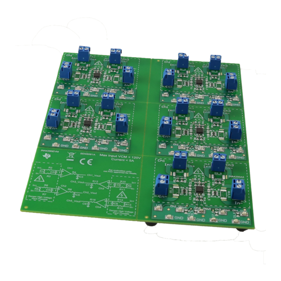
Hardware 3 Hardware The INA4290EVM provides a basic functional evaluation of the INA4290. The fixture layout is not intended to be a model for the target circuit, nor is it laid out for electromagnetic compatibility (EMC) testing. The INA4290EVM is one PCB with five optional PCB cutouts the engineer can use to test each of the five gain options (1 to 5) -
Page 6: Operation
4.1 Quick Start Setup Follow these procedures to set up and use one of the INA4290EVM panels. For these instructions, n is gain option 1, 2, 3, 4, or 5 and x is the channel option 1, 2, 3, or 4. -
Page 7: Evm Components
EVM Components 5 EVM Components This section summarizes the INA4290EVM components. For these instructions, n is gain option 1, 2, 3, 4, or 5. 5.1 R2_n, R3_n, R4_n, R6_n, R7_n, R8_n, R10_n, R11_n, R14_n, R15_n, C2_n - C9_n R2_n, R3_n, R4_n, R6_n, R7_n, R8_n are factory-installed 0-Ω 0603 resistors. -
Page 8: Schematic, Pcb Layout, And Bill Of Materials
INA4290EVM PCB manufacturing. 6.1 Schematics Figure 6-1 through Figure 6-5 show the schematics for the A pinout of the INA4290EVM PCB for all gain options. Figure 6-1. INA4290EVM Schematic: Gain A1 Panel INA4290 Evaluation Module SBOU258 – MARCH 2021 Submit Document Feedback... -
Page 9: Figure 6-2. Ina4290Evm Schematic: Gain A2
Schematic, PCB Layout, and Bill of Materials Figure 6-2. INA4290EVM Schematic: Gain A2 Panel SBOU258 – MARCH 2021 INA4290 Evaluation Module Submit Document Feedback Copyright © 2021 Texas Instruments Incorporated... -
Page 10: Figure 6-3. Ina4290Evm Schematic: Gain A3
Schematic, PCB Layout, and Bill of Materials www.ti.com Figure 6-3. INA4290EVM Schematic: Gain A3 Panel INA4290 Evaluation Module SBOU258 – MARCH 2021 Submit Document Feedback Copyright © 2021 Texas Instruments Incorporated... -
Page 11: Figure 6-4. Ina4290Evm Schematic: Gain A4 Panel
Schematic, PCB Layout, and Bill of Materials Figure 6-4. INA4290EVM Schematic: Gain A4 Panel SBOU258 – MARCH 2021 INA4290 Evaluation Module Submit Document Feedback Copyright © 2021 Texas Instruments Incorporated... -
Page 12: Figure 6-5. Ina4290Evm Schematic: Gain A5
Schematic, PCB Layout, and Bill of Materials www.ti.com Figure 6-5. INA4290EVM Schematic: Gain A5 Panel INA4290 Evaluation Module SBOU258 – MARCH 2021 Submit Document Feedback Copyright © 2021 Texas Instruments Incorporated... -
Page 13: Pcb Layout
Schematic, PCB Layout, and Bill of Materials 6.2 PCB Layout Figure 6-6 through Figure 6-12 show the PCB layout for the INA4290EVM. Figure 6-6. INA4290EVM Top Overlay Figure 6-7. INA4290EVM Bottom Overlay Figure 6-8. INA4290EVM Top Layer Figure 6-9. INA4290EVM Bottom Layer SBOU258 –... -
Page 14: Figure 6-10. Ina4290Evm Top Solder
Schematic, PCB Layout, and Bill of Materials www.ti.com Figure 6-10. INA4290EVM Top Solder Figure 6-11. INA4290EVM Bottom Solder Figure 6-12. INA4290EVM Drill Drawing INA4290 Evaluation Module SBOU258 – MARCH 2021 Submit Document Feedback Copyright © 2021 Texas Instruments Incorporated... -
Page 15: Bill Of Materials
Schematic, PCB Layout, and Bill of Materials 6.3 Bill of Materials Table 6-1 provides the parts list for the INA4290EVM. Table 6-1. Bill of Materials DESIGNATOR VALUE DESCRIPTION PACKAGE REFERENCE PART NUMBER MANUFACTURER C1_1, C1_2, C1_3, C1_4, C1_5 0.1uF CAP, CERM, 0.1 uF, 25 V, ±10%, X7R,... - Page 16 R1_1, R1_2, R1_3, R1_4, R1_5, R5_1, R5_2, R5_3, R5_4, 0.01 RES, 0.01, 1%, 3 W, 2512 2512 CRA2512-FZ-R010ELF Bourns R5_5, R9_1, R9_2, R9_3, R9_4, R9_5, R13_1, R13_2, R13_3, R13_4, R13_5 INA4290 Evaluation Module SBOU258 – MARCH 2021 Submit Document Feedback Copyright © 2021 Texas Instruments Incorporated...
- Page 17 TI products. TI’s provision of these resources does not expand or otherwise alter TI’s applicable warranties or warranty disclaimers for TI products. TI objects to and rejects any additional or different terms you may have proposed. IMPORTANT NOTICE Mailing Address: Texas Instruments, Post Office Box 655303, Dallas, Texas 75265 Copyright © 2022, Texas Instruments Incorporated...
Need help?
Do you have a question about the INA4290EVM and is the answer not in the manual?
Questions and answers