Table of Contents
Advertisement
UM2819
User manual
STM32WB Nucleo-64 board (MB1355)
Introduction
®
The NUCLEO-WB55RG STM32WB Nucleo-64 board based on the MB1355 board is a Bluetooth
Low Energy wireless
®
and ultra-low-power device embedding a powerful and ultra-low-power radio compliant with the Bluetooth
Low Energy SIG
specification v5.2 and IEEE802.15.4-2011 PHY and MAC is supported.
®
The ARDUINO
Uno V3 connectivity support and the ST morpho headers provide an easy means of expanding the functionality
of the STM32WB Nucleo open development platform with a wide choice of specialized shields.
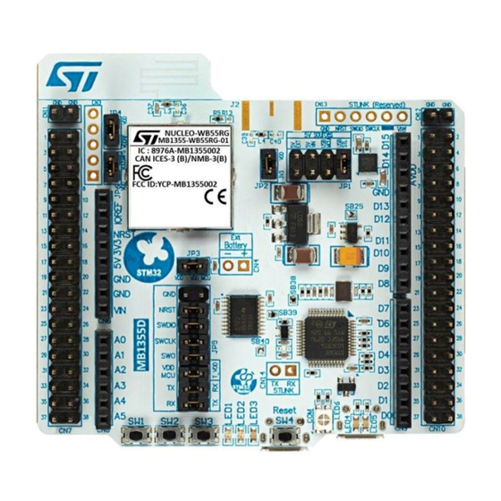
Figure 1.
NUCLEO-WB55RG top view
Picture is not contractual.
UM2819 - Rev 1 – March 2022
www.st.com
For further information contact your local STMicroelectronics sales office.
Advertisement
Table of Contents

Related Manuals for ST NUCLEO-WB55RG STM32WB


Summary of Contents for ST NUCLEO-WB55RG STM32WB
-
Page 1: Figure 1. Nucleo-Wb55Rg Top View
IEEE802.15.4-2011 PHY and MAC is supported. ® The ARDUINO Uno V3 connectivity support and the ST morpho headers provide an easy means of expanding the functionality of the STM32WB Nucleo open development platform with a wide choice of specialized shields. Figure 1. -
Page 2: Features
Board connectors: – ® ARDUINO Uno V3 expansion connector – ST morpho extension pin headers for full access to all STM32WB I/Os • Integrated PCB antenna and SMA connector footprint • Flexible power-supply options: ST-LINK, USB V , or external sources •... -
Page 3: Ordering Information
UM2819 Ordering information Ordering information To order the NUCLEO-WB55RG Nucleo-64 board, refer to Table 1. Additional information is available from the datasheet and reference manual of the target STM32. Table 1. Ordering information Order code Board reference Target STM32 NUCLEO-WB55RG MB1355 STM32WB55RG Codification... -
Page 4: Development Environment
STM32 Flash memory for easy demonstration of the device peripherals in standalone mode. The latest versions of the demonstration source code and associated documentation can be downloaded from www.st.com. UM2819 - Rev 1 page 4/37... -
Page 5: Conventions
UM2819 Conventions Conventions Table 3 provides the conventions used for the ON and OFF settings in the present document. Table 3. ON/OFF convention Convention Definition Jumper JPx ON Jumper fitted Jumper JPx OFF Jumper not fitted Jumper JPx [1-2] Jumper fitted between Pin 1 and Pin 2 SBx connections closed by 0 Ω... -
Page 6: Safety Recommendations
UM2819 Safety recommendations Safety recommendations Targeted audience This product targets users with at least basic electronics or embedded software development knowledge such as engineers, technicians, or students. This board is not a toy and is not suited for use by children. Handling the board This product contains a bare printed circuit board and like all products of this type, the user must be careful about the following points:... -
Page 7: Quick Start
Connect the Nucleo board to a PC with a USB Type-A or USB Type-C to Micro-B cable through CN15 USB ST-LINK connector. Once powered on, the LD2 green LED blinks for each advertising interval – timeout after one minute. ®... -
Page 8: Hardware Layout And Configuration
Figure 2 illustrates the connection between NUCLEO-WB55RG and its peripherals (ARDUINO Uno V3 connector, ST morpho connector, and embedded ST-LINK). Figure 3 Figure 5 help the user to locate these features on the NUCLEO-WB55RG board. The mechanical... -
Page 9: Figure 3. Nucleo-Wb55Rg Pcb Top Side
CN15 USB_STLINK LD1, LD2, LD3 user LEDs U8 STLINK MCU CN1 USB_MCU LD6 STLINK Status B4 Reset push-button ST Restricted Figure 4. NUCLEO-WB55RG PCB with details of the main part (SoC and RF) MLPF-WB55-01E3 HSE Crystal (32MHz) (Matching Network & Filter) U1 STM32WB55RG LSE Crystal (32.768KHz) -
Page 10: Figure 5. Nucleo-Wb55Rg Pcb Bottom Side
UM2819 Hardware layout and configuration Figure 5. NUCLEO-WB55RG PCB bottom side Footprint for CR2032 battery socket (optional: not assembly by default) SW5 Switch for external power supply CN15 USB_STLINK USB_MCU UM2819 - Rev 1 page 10/37... -
Page 11: Figure 6. Nucleo-Wb55Rg Mechanical Dimensions (In Millimeters)
UM2819 Hardware layout and configuration Figure 6. NUCLEO-WB55RG mechanical dimensions (in millimeters) UM2819 - Rev 1 page 11/37... -
Page 12: Power Supply
® ARDUINO shield which can deliver this type of voltage on the VIN pin. VIN CN7 pin 24 of the ST morpho connector. It is possible to apply until +12 V on this pin like for the ® ARDUINO connection. -
Page 13: Power Supply
ST-LINK/V2 and Virtual COM port and therefore can get supply from the host computer. It is also possible to connect a USB charger to this connector. In this case, the ST-LINK and the VCP cannot be accessible. -
Page 14: Current Measurement
Close SB17 Open Ext (CN4-1) SB20 Close SB16 Open SB19 Optional CR2032 Socket (CN2) VBAT Open JP1(5-6) USB MCU (CN1) VDDSMPS JP1(7-8) Close USB STLNK (CN15) Close STM32F103 (STLINK MCU) LDO 3V3 ST Restricted UM2819 - Rev 1 page 14/37... -
Page 15: Clock Sources
The NUCLEO-WB55RG reset signal is active LOW. The internal pull-up resistor forces the RST signal to a high level. The sources of reset are: • B4 reset push button • Embedded ST-LINK/V2-1 • ® ® CN2 ARDUINO connector pin 3 (ARDUINO board reset). • CN7 ST morpho connector pin 14 UM2819 - Rev 1 page 15/37... -
Page 16: Embedded St-Link/V2-1
7.4.2 ST-LINK/V2-1 firmware upgrade The ST-LINK/V2-1 embeds a firmware upgrade mechanism for the in-situ upgrade through the USB port. As the firmware may evolve during the lifetime of the ST-LINK/V2-1 product (for example new functionalities, bug fixes, support for new microcontroller families), it is recommended to visit the www.st.com... -
Page 17: Virtual Com Port: Usart1
3.3 V sources. By default, STM32WB55RG is supplied by the same voltage value as ST-LINK, but it is possible to supply the SoC with another value. It accepts a voltage between 1.8 and 3.3 V trust to a level shifter. -
Page 18: Jp5 Multi-Function Jumper
Embedded ST-LINK/V2-1 7.4.7 JP5 multi‑function jumper The JP5 multi‑function jumper can connect ST-LINK/V2-1 to STM32WB55RG. It is located between the level shifter and the SoC. It is referenced to the VDD domain (STM32WB55RG supply voltage domain). Figure 11. Interconnection bloc diagram between STM32WB55RG and ST-LINK/V2-1... -
Page 19: Leds
– Slow blinking red and OFF: at power-on, before USB initialization – Fast blinking red and OFF: after the first correct communication between the host PC and ST-LINK/ V2-1 (enumeration) – Red ON: when initialization between the host PC and ST-LINK/V2-1 is successfully finished. -
Page 20: Push-Buttons
UM2819 Push-buttons Push-buttons 7.6.1 Description NUCLEO-WB55RG provides two types of buttons: • B1 USER1 pushbutton • B2 USER2 pushbutton • B3 USER3 pushbutton • B4 reset pushbutton to reset the NUCLEO-WB55RG board. Figure 13. Push-buttons location B1, user Pushbutton B2, user Pushbutton B3, user Pushbutton B4, reset Pushbutton 7.6.2... -
Page 21: Rf I/O Stage
® Note that PA0 is also connected to ARDUINO and ST morpho connectors as GPIO, depending on the use case that can generate conflict with B1. In this case, it possible to remove the connection of B1 (SB11 OFF). Table 8. -
Page 22: Embedded Smps
UM2819 Embedded SMPS Embedded SMPS NUCLEO-WB55RG embeds an SMPS to optimize the power consumption. All the details of this part are explained in the datasheet and the reference manual of the NUCLEO-WB55RG. NUCLEO-WB55RG allows the evaluation of the SoC with this SMPS active. All the components necessary for the operation are present. Moreover, it is possible to bypass the SMPS. -
Page 23: Arduino Connector
UM2819 ARDUINO® and MORPHO connectors ® ARDUINO connector 7.9.1 Description ® On the bottom side of the board, there is an ARDUINO Uno V3 extension socket. It is built around four standard ® CN5, CN6, CN8, and CN9 connectors. Most shields designed for ARDUINO can fit with the development boards to offer flexibility in small form factor applications. -
Page 24: Arduino ® Interface And Pinout
Figure 17. ARDUINO connector location and pinout NUCLEO-WB55RG AVDD CN5 digital 8-15 ARDUINO ® IOREF CN6 power ARDUINO ® NRST CN9 digital 0-7 ARDUINO ® CN8 analog 0-5 ARDUINO ® Arduino Uno Shield ST Res UM2819 - Rev 1 page 24/37... -
Page 25: Table 9. Arduino ® Connector Pinout
UM2819 ARDUINO® and MORPHO connectors ® Table 9. ARDUINO connector pinout Connector Pin number Signal name STM32 pin Comment Not connected (Reserved for the test) 3V3 (IOREF) IOREF 3.3 V NRST NRST NRST 3.3 V External Supply Input (+12 V) ADC1_IN9 ADC1_IN11 ADC1_IN6... -
Page 26: Nucleo-Wb55Rg I/O Assignment
NUCLEO-WB55RG I/O assignment The CN7 and CN10 ST morpho connectors are male pin headers accessible on both sides of the board. All signals and power pins of the MCU are available on these ST morpho connectors. These connectors can also be probed by an oscilloscope, logical analyzer, or voltmeter. -
Page 27: Table 10. St Morpho Connectors Pinout
UM2819 ARDUINO® and MORPHO connectors Table 10. ST morpho connectors pinout CN10 STM32WB55RGpi STM32WB55RG STM32WB55RG STM32WB55RG number n name number pin name number pin name number pin name PB11 5V_EXT BOOT0 AVDD 5V_USB_MCU 5V_INT (with 1 kΩ resistor) PA12 PA13... -
Page 28: Nucleo-Wb55Rg Board Information
Evaluation tools marked as “ES” or “E” are not yet qualified and therefore not ready to be used as reference design or in production. Any consequences deriving from such usage will not be at ST charge. In no event, ST will be liable for any customer usage of these engineering sample tools as reference designs or in production. -
Page 29: Federal Communication Commission (Fcc)
UM2819 Federal Communication Commission (FCC) Federal Communication Commission (FCC) Identification of products: NUCLEO-WB55RG. FCC ID: YCP-MB1355002 Part 15.19 This device complies with Part 15 of the FCC Rules. Operation is subject to the following two conditions: (1) this device may not cause harmful interference, and (2) this device must accept any interference received, including interference that may cause undesired operation. -
Page 30: Innovation, Science And Economic Development Canada (Ised) Compliance Statements
UM2819 Innovation, Science and Economic Development Canada (ISED) Compliance Statements Innovation, Science and Economic Development Canada (ISED) Compliance Statements This radio transmitter (8976A-MB1355002) has been approved by Industry Canada to operate with the antenna types listed below with the maximum permissible gain and required antenna impedance for each antenna type indicated. -
Page 31: Red Compliance Statement
UM2819 RED compliance statement RED compliance statement Déclaration de conformité CE simplifiée : STMicroelectronics déclare que l'équipement radioélectrique du type " NUCLEO-WB55RG " est conforme à la directive 2014/53/UE. Bande de fréquence utilisée en transmission et puissance maximale rayonnée dans cette bande : •... -
Page 32: Revision History
UM2819 Revision history Table 11. Document revision history Date Version Changes 04-Mar-22 Initial release. UM2819 - Rev 1 page 32/37... -
Page 33: Table Of Contents
Reset sources ........................... 15 Embedded ST-LINK/V2-1 ....................... 16 7.4.1 Drivers .............................. 16 7.4.2 ST-LINK/V2-1 firmware upgrade ....................16 7.4.3 CN15 ST-LINK/V2-1 USB connector ................... 16 7.4.4 Virtual COM port: USART1 ......................17 7.4.5 Level shifter ............................17 7.4.6 JP5 multi‑function jumper ......................17 LEDs .............................. - Page 34 UM2819 Contents RF I/O stage ............................21 Embedded SMPS ..........................22 ® ARDUINO connector ........................23 7.9.1 Description ............................23 7.9.2 Operating voltage ..........................23 ® 7.9.3 ARDUINO interface and pinout ....................24 7.9.4 NUCLEO-WB55RG I/O assignment ..................... 26 NUCLEO-WB55RG board information ..................28 Product marking ..........................
-
Page 35: List Of Tables
Table 7. Multi-function jumper pinout description ..........................18 Table 8. I/O configuration for the physical user interface........................21 ® Table 9. ARDUINO connector pinout ..............................25 Table 10. ST morpho connectors pinout ..............................27 Table 11. Document revision history.................................32 UM2819 - Rev 1 page 35/37... -
Page 36: List Of Figures
Figure 9. Current measurement with an external power supply .......................15 Figure 10. USB composite device ................................16 Figure 11. Interconnection bloc diagram between STM32WB55RG and ST-LINK/V2-1 ..............17 Figure 12. LEDs location ..................................19 Figure 13. Push-buttons location ................................20 Figure 14. - Page 37 ST’s terms and conditions of sale in place at the time of order acknowledgement. Purchasers are solely responsible for the choice, selection, and use of ST products and ST assumes no liability for application assistance or the design of Purchasers’...
Need help?
Do you have a question about the NUCLEO-WB55RG STM32WB and is the answer not in the manual?
Questions and answers