Table of Contents
Advertisement
UM2910
User manual
STLINK-V3MINIE debugger/programmer tiny probe for STM32 microcontrollers
Introduction
STLINK-V3MINIE
is a stand-alone debugging and programming tiny probe for STM32 microcontrollers.
The JTAG/SWD interfaces are used to communicate with any STM32 microcontroller located on an application board.
STLINK-V3MINIE also provides a Virtual COM port interface for the host PC to communicate with the target microcontroller
through one UART.
STLINK-V3MINIE is a portable version easy‑to‑use debugger and programmer including STDC14 interface with its flat cable
and on‑board pads for board‑to‑board (BTB) card edge connector.
Figure 1.
STLINK-V3MINIE top, bottom, and cable views
Pictures are not contractual.
UM2910 - Rev 2 - January 2022
www.st.com
For further information contact your local STMicroelectronics sales office.
Advertisement
Table of Contents

Related Manuals for ST STLINK-V3MINIE


Summary of Contents for ST STLINK-V3MINIE
-
Page 1: Figure 1. Stlink-V3Minie Top, Bottom, And Cable Views
STM32 microcontrollers. The JTAG/SWD interfaces are used to communicate with any STM32 microcontroller located on an application board. STLINK-V3MINIE also provides a Virtual COM port interface for the host PC to communicate with the target microcontroller through one UART. -
Page 2: Features
1.27 mm pitch STDC14 debug connector with STDC14 to STDC14 flat cable – 2.0 mm pitch on-board pads for BTB (Board-to-board) card edge connector Note: STLINK-V3MINIE does not provide any power supply to the target application. UM2910 - Rev 2 page 2/20... -
Page 3: Ordering Information
UM2910 Ordering information Ordering information To order the STLINK-V3MINIE tiny probe, refer to Table Table 1. Ordering information Order code Content and references Description • MB1762 • STLINK-V3 in-circuit debugger and programmer for STLINK-V3MINIE STM32 microcontrollers with level shifter •... -
Page 4: Development Environment
Firmware upgrade The STLINK-V3MINIE tiny probe embeds firmware that needs to be frequently updated from the www.st.com website to benefit from new functionality or corrections. Refer to the technical note Overview of ST-LINK derivatives (TN1235) for details. UM2910 - Rev 2... -
Page 5: Quick Start
Before installing and using these products, accept the Evaluation Product License Agreement from the www.st.com/epla web page. The STLINK-V3MINIE tiny probe is a stand-alone debugging and programming probe for STM32 microcontrollers: • It supports JTAG and SWD protocols to communicate with any STM32 microcontroller. -
Page 6: Stlink-V3Minie Functional Description
VCP (From 736 bps to 16 Mbps) A double‑row, 14‑pin (2 × 7) 1.27 mm pitch male STDC14 connector is located in STLINK-V3MINIE for connection to the application target. An STDC14 to STDC14 flat cable is included in the packaging. -
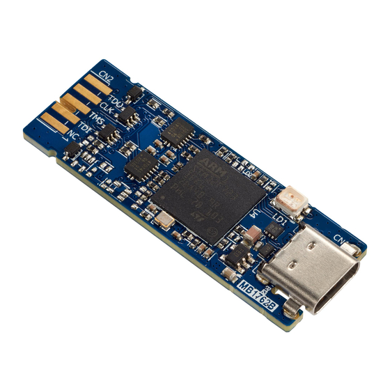
Page 7: Figure 3. Mb1762 Top Layout
UM2910 Hardware layout Figure 3. MB1762 top layout USB Type-C ® connector (CN1) COM LED (LD1) Power LED (LD2) STM32F723 microcontroller (U4) Pads for BTB connector (Top) (CN2) Figure 4. MB1762 bottom layout STDC14 connector (CN4) Pads for BTB connector (Bottom) (CN2) UM2910 - Rev 2 page 7/20... -
Page 8: Figure 5. Mb1762 Mechanical Drawing (In Millimeters)
UM2910 Hardware layout Figure 5. MB1762 mechanical drawing (in millimeters) UM2910 - Rev 2 page 8/20... -
Page 9: Stlink-V3Minie Functions
5.5.3 Virtual COM port (VCP) The serial interface VCP is directly available as a Virtual COM port of the PC, connected to the STLINK-V3MINIE CN1 USB connector. This function may be used for STM32 microcontrollers. The signals may perform from 736 bps to 16 Mbps. -
Page 10: Board Connectors
Pads on board to CN2 BTB card edge connector The pads on the board have the same function as the STDC14 connector. The user can select a BTB card edge connector to connect STLINK-V3MINIE and the target board. The board‑to‑board card edge connector reference is 009159010061911 from AVX. -
Page 11: Cn4 Stdc14 Connector
UM2910 CN4 STDC14 connector CN4 STDC14 connector The CN4 STDC14 connector allows the connection to an STM32 target using the JTAG or SWD protocol, ® ® respecting from pin 3 to pin 12 the MIPI‑10 (Arm Cortex debugging connector) pinout. It also advantageously provides two UART signals for the Virtual COM port. -
Page 12: Performance Figures
Performance figures Table 5 gives an overview of the achievable maximal performances with STLINK-V3MINIE on different communication channels. Those performances are also depending on the overall system context (target included), so they are not guaranteed to be always reachable. For instance, a noisy environment or the connection quality can impact system performance. -
Page 13: Stlink-V3Minie Board Information
Evaluation tools marked as “ES” or “E” are not yet qualified and therefore not ready to be used as reference design or in production. Any consequences deriving from such usage will not be at ST charge. In no event, ST will be liable for any customer usage of these engineering sample tools as reference designs or in production. -
Page 14: Federal Communications Commission (Fcc) And Innovation, Science And Economic
UM2910 Federal Communications Commission (FCC) and Innovation, Science and Economic Development Canada (ISED) Compliance Statements Federal Communications Commission (FCC) and Innovation, Science and Economic Development Canada (ISED) Compliance Statements FCC Compliance Statement Part 15.19 This device complies with Part 15 of the FCC Rules. Operation is subject to the following two conditions: (1) this device may not cause harmful interference, and (2) this device must accept any interference received, including interference that may cause undesired operation. -
Page 15: Revision History
UM2910 Revision history Table 6. Document revision history Date Version Changes 20-Oct-2021 Initial release. Added: • Performance figures Updated: • Features 19-Jan-2022 • Ordering information • Section 3.3 Firmware upgrade • Figure Figure Figure 4, and Figure 5 • Section 5.5.4 Mass-storage interface ®... -
Page 16: Table Of Contents
STLINK-V3MINIE functional description ........ - Page 17 UM2910 Contents List of tables ................18 List of figures.
- Page 18 CN4 STDC14 connector pinout ............11 Table 5. Achievable maximal performance with STLINK-V3MINIE on different channels ......12 Table 6.
- Page 19 STLINK-V3MINIE top, bottom, and cable views........
- Page 20 ST’s terms and conditions of sale in place at the time of order acknowledgement. Purchasers are solely responsible for the choice, selection, and use of ST products and ST assumes no liability for application assistance or the design of Purchasers’...
Need help?
Do you have a question about the STLINK-V3MINIE and is the answer not in the manual?
Questions and answers