Table of Contents
Advertisement
Quick Links
Colour Television
Contents
11. Styling Sheets
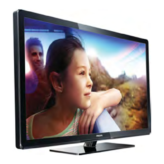
3000 series 32"
3000 series 42"
Published by XjL/MjX/MC/SC 1266 TV Quality
©
2012
TP Vision Netherlands B.V.
All rights reserved. Specifications are subject to change without notice. Trademarks are the
property of Koninklijke Philips Electronics N.V. or their respective owners.
TP Vision Netherlands B.V. reserves the right to change products at any time without being obliged to adjust
earlier supplies accordingly.
PHILIPS and the PHILIPS' Shield Emblem are used under license from Koninklijke Philips Electronics N.V.
Page
2
2
5
9
24
26
30
37
38
39
Drawing PWB
38
59-60
61
62
63
64
67
68
Printed in the Netherlands
Chassis
TPM9.1A
Subject to modification
EN 3122 785 19330
LA
Advertisement
Table of Contents

Related Manuals for Philips 32PFL3007


Summary of Contents for Philips 32PFL3007
-
Page 1: Table Of Contents
Koninklijke Philips Electronics N.V. or their respective owners. TP Vision Netherlands B.V. reserves the right to change products at any time without being obliged to adjust earlier supplies accordingly. PHILIPS and the PHILIPS’ Shield Emblem are used under license from Koninklijke Philips Electronics N.V. -
Page 2: Revision List
& Notes: drivers. • Figures can deviate due to the different set executions. Table 2-1 Described Model Numbers and Diversity Mechanics Block Diagrams Schematics 32PFL3007/56 4.3.1 4.3.4 10.1 10.2 10.3 11.1 32PFL3007/98 4.3.1 4.3.4... - Page 3 Technical Specs, Diversity, and Connections TPM9.1AL LA EN 3 Connections TV ANTENNA AUDIO PC IN HDMI 2 CVI 2/AV SERV.U HDMI 1 VIDEO AV OUT CVI 1 19330_001_120608.eps 120612 Figure 2-1 Connection overview Note: The following connector colour abbreviations are used Rd - Audio R 0.5 V / 10 k...
- Page 4 EN 4 TPM9.1AL LA Technical Specs, Diversity, and Connections 18 - +5V 13 - H-sync 0 - 5 V 19 - HPD Hot Plug Detect 14 - V-sync 0 - 5 V 20 - Ground 15 - DDC_SCL DDC clock 2.3.2 Rear Connections 9 - HDMI 2: Digital Video - In, Digital Audio with ARC -...
-
Page 5: Precautions, Notes, And Abbreviation List
3.3.3 Spare Parts external damage. • Check the strain relief of the Mains/AC Power cord for For the latest spare part overview, consult your Philips Spare proper function. Part web portal. • Check the electrical DC resistance between the Mains/AC... - Page 6 EN 6 TPM9.1AL LA Precautions, Notes, and Abbreviation List The third digit in the serial number (example: Abbreviation List AG2B0335000001) indicates the number of the alternative B.O.M. (Bill Of Materials) that has been used for producing the 0/6/12 SCART switch control signal on A/V specific TV set.
- Page 7 6.5 MHz. L' is Band (VESA standard for communication I, L is all bands except for Band I channel and display). Using E-DDC, LG.Philips LCD (supplier) the video source can read the EDID Loudspeaker information form the display.
- Page 8 SOPS Self Oscillating Power Supply Serial Peripheral Interface bus; a 4-wire synchronous serial data link standard S/PDIF Sony Philips Digital InterFace SRAM Static RAM Service Reference Protocol Small Signal Board Spread Spectrum Clocking, used to reduce the effects of EMI...
-
Page 9: Mechanical Instructions
Mechanical Instructions TPM9.1AL LA EN 9 4. Mechanical Instructions Index of this chapter: Notes: 4.1 Cable Dressing • Figures below can deviate slightly from the actual situation, 4.2 Service Positions due to the different set executions. 4.3 Assembly/Panel Removal 4.4 Set Re-assembly Cable Dressing 19330_100_120608.eps 120608... - Page 10 EN 10 TPM9.1AL LA Mechanical Instructions 19330_101_120608.eps 120611 Figure 4-2 Cable dressing (42") Service Positions For easy servicing of a TV set, the set should be put face down on a soft flat surface, foam buffers or other specific workshop tools.
- Page 11 Mechanical Instructions TPM9.1AL LA EN 11 M4 × 8 Q4 × 16 Q3 × 8 19330_102_120612.eps 120612 Figure 4-3 Rear cover removal 4.3.2 Stand Refer to Figure 4-4 for details. 1. Remove fixation screws [4] that secure the base assembly, pull the base assembly downwards away from the catches.
- Page 12 EN 12 TPM9.1AL LA Mechanical Instructions M4 × 18 19330_104_120612.eps 120612 Figure 4-4 Stand removal 4.3.3 Power Supply Unit (PSU) Caution: it is mandatory to remount all different screws at their original position during re-assembly. Failure to do so may result in damaging the PSU.
- Page 13 Mechanical Instructions TPM9.1AL LA EN 13 4.3.6 Keyboard Control unit 1. Unplug the connector from the keyboard control panel. 2. Gently push inwards the two clips at the PSU side of the unit. Release the unit at the PSU side and turn it away from the PSU.
-
Page 14: Service Modes, Error Codes, And Fault Finding
EN 14 TPM9.1AL LA Service Modes, Error Codes, and Fault Finding 5. Service Modes, Error Codes, and Fault Finding Index of this chapter: Life Timer 5.1 Test Points During the life time cycle of the TV set, a timer is kept (called 5.2 Service Modes “Op. - Page 15 Service Modes, Error Codes, and Fault Finding TPM9.1AL LA EN 15 – Automatic user menu time-out (menu switches controls will not have I+ button, but an “INFO” button back/OFF automatically. instead. – Auto Volume levelling (AVL). How to Exit SDM How to Activate SDM •...
- Page 16 EN 16 TPM9.1AL LA Service Modes, Error Codes, and Fault Finding Main Menu Sub-menu 1 Sub-menu 2 Description Download from USB Copy Channel List from USB To download several settings from the USB stick to the TV Copy NVM from USB Copy Readable Info from USB Copy EDID from USB Initialize NVM...
- Page 17 Service Modes, Error Codes, and Fault Finding TPM9.1AL LA EN 17 Default value Item Item value 32" 42" Description CLR_TEMP_G Green colour temperature setting CLR_TEMP_B Red colour temperature setting AUTO_COLOR Press OK PC: any pattern that has black and white, YPbPr: SMPTE bar (colour bar), any timing. ADC_GAIN_R Red ADC gain ADC_GAIN_G...
- Page 18 EN 18 TPM9.1AL LA Service Modes, Error Codes, and Fault Finding Note: When the TV is switched “off” by a power interrupt, or • 3.2 Child lock Not active / active. This is a combined item normal switch to “stand-by” while in the factory mode, the TV for locks.
- Page 19 Service Modes, Error Codes, and Fault Finding TPM9.1AL LA EN 19 Stepwise Start-up Standby Soft Mode Command Received, Switch previously in Standby Off(Mains Soft Mode (Power tact Standby Power Plug) switch) Digital Digital background background tasks started tasks completed TV Wakeup commands Received Standby...
- Page 20 A description on how to upgrade the main 1. ComPair helps to quickly get an understanding on how to software can be found in the DFU or on the Philips website. repair the chassis in a short and effective way.
- Page 21 Service Modes, Error Codes, and Fault Finding TPM9.1AL LA EN 21 • FUS_clustername_version.zip: Contains the “autorun.upg” which is needed to upgrade the TV main software and the software download application. • NVM_clustername_version.zip: Default NVM content. Must be programmed via ComPair. 5.5.7 How to Copy NVM Data to/from USB When copying data to and from a USB memory stick, the folder...
- Page 22 EN 22 TPM9.1AL LA Service Modes, Error Codes, and Fault Finding – ERROR: 034 013 000 000 000: Error code 13 was • It is assumed that the components are mounted correctly detected first and error code 34 is the last detected with correct values and no bad solder joints.
- Page 23 Service Modes, Error Codes, and Fault Finding TPM9.1AL LA EN 23 5.8.10 Display option code Attention: In case the SSB is replaced, always check the Panel Code in CSM, even when picture is available. Performance with the incorrect display option code can lead to unwanted side-effects for certain conditions.
-
Page 24: Alignments
US/AP-NTSC models: an NTSC M/N TV-signal with a Picture mode Screen size Green Blue signal strength of at least 1 mV and a frequency of Normal (9000K) 32PFL3007 61.25 MHz (channel 3). 42PFL3007 • LATAM models: an NTSC M TV-signal with a signal Cool (11000K) 32PFL3007... - Page 25 6-3. After resetting the Display Code, restart the set immediately. Table 6-3 Display code overview CTN_ALT BOM# Panel Type Display Code 32PFL3007 T315XW04 V384 42PFL3007 LCD LC420WUE-SCV1 Reset of Repaired SSB A very important issue towards a repaired SSB from a Service repair shop (SSB repair on component level) implies the reset of the NVM on the SSB.
-
Page 26: Circuit Descriptions
7.4 Front-End Analogue and reception 7.5 HDMI Philips 3007 series comes with the following stylings: 7.6 Video and Audio Processing - MT5301B • Philips 3007 series be supported for 1920 × 1080 full-HD • Panel (3007 series 32PFL3007/42PFL3007) Notes: •... - Page 27 Circuit Descriptions TPM9.1AL LA EN 27 7.1.3 SSB Cell Layout DC/DC MT5301B Headphone TUNER HDMI SWITCH AV IN ANALOG I/O CVI/AV AV OUT HDMI HDMI 19330_200_120611.eps 120612 Figure 7-1 SSB layout cells (top view) back to 2012-Jun-15 div. table...
- Page 28 This part is available in the regular market. PSL stands for Power Supply with integrated LED-drivers. Consult the Philips Service web portal for the order codes of the PSLS stands for a Power Supply with integrated LED-drivers boards.
- Page 29 Circuit Descriptions TPM9.1AL LA EN 29 • AVDD 1V2,from the power supply for the scaler IC MT5301B • +1V2, supply voltage for power supply for the scaler IC HDMI 1 MT5301B • DDRV (+1.8V) supply voltage for DDR2 TMDS • V3.3 V1.2 supply voltage for DEMOD MT5301B HDMI 2...
-
Page 30: Ic Data Sheets
EN 30 TPM9.1AL LA IC Data Sheets 8. IC Data Sheets This chapter shows the internal block diagrams and pin configurations of ICs that are drawn as “black boxes” in the electrical diagrams (with the exception of “memory” and “logic” ICs). - Page 31 IC Data Sheets TPM9.1AL LA EN 31 Pinning information FSRC_WR 192 AVDD33_XTAL_STB GPIO14 191 XTALI VCC3IO 190 XTALO AVDD12_VPLL 189 AVDD33_DEMOD AE5P 188 AVSS33_DEMOD AE5N 187 AVSS12_DEMOD AE4P 186 AVDD33_IFPGA AE4N 185 ADCINN_DEMOD AE3P 184 ADCINP_DEMOD AE3N 183 AVDD12_DEMOD AECKP 182 AVDD33_CVBS AECKN 181 CVBS0P...
- Page 32 EN 32 TPM9.1AL LA IC Data Sheets Diagram 10-1-9 B09, HDMI A & Switch 3:1, TMDS361BPAGR (IC U501) Block diagram Dx+_1 TMDS361B TMDS Rx w/ AEQ Dx–_1 CLK+_1 TMDS Rx CLK–_1 Clock Detect VSadj SCL1 Dx+_SINK TMDS Tx Dx–_SINK SDA1 CLK+_SINK TMDS Tx CLK–_SINK...
- Page 33 IC Data Sheets TPM9.1AL LA EN 33 Diagram 10-1-16 B16, Headphone Out, TPA6132A2RTER (IC U606) Block diagram HPVDD TPA6132A2RTER Supply 2.2 F Control PGND HPVDD INL- Resistor OUTL Array INL+ Short-Circuit HPVSS Protection Thermal HPVDD Protection INR- Resistor OUTR Array INR+ HPVDD HPVSS...
- Page 34 EN 34 TPM9.1AL LA IC Data Sheets Diagram 10-1-17 B17, I2S Post amplifier & S/PDIF Out, AD82586 (IC U4104) Block diagram C Control Logic ERROR Interface Interface Internal BCLK AD82586 System Input SDATA Clock Interface LRCIN Loudspeaker Audio Signal PCM to PWM Driver Processing Pinning information...
-
Page 35: Block Diagrams
Block Diagrams TPM9.1A LA EN 35 9. Block Diagrams Wiring diagram 3000 32" WIRING DIAGRAM 32" (3000) Board Level Repair Component Level Repair Component Level Repair Component Level Repair Only for authorized workshops Only for authorized workshops Only for authorized workshops to panel CN701 CN902... -
Page 36: Wiring Diagram 3000 42
Block Diagrams TPM9.1A LA EN 36 Wiring diagram `3000 42" WIRING DIAGRAM 42" (3000) Board Level Repair Component Level Repair Component Level Repair Component Level Repair Only for authorized workshops Only for authorized workshops Only for authorized workshops to panel to panel to panel CN902... -
Page 37: Block Diagram 3000
Block Diagrams TPM9.1A LA EN 37 Block Diagram 3000 DDR III × 1 SPI FLASH NAND FLASH 128M × 16b 8M Byte 32MB 1333 MHz Digital Demodulator IF+/- D+A RF ATBM8846E LCD PANEL (PARALLEL) TUNER Analog IF+/- LVDS (50/60 Hz) TUNER Demodulator PC IN... -
Page 38: Circuit Diagrams And Pwb Layouts
Circuit Diagrams and PWB Layouts TPM9.1A LA EN 38 10. Circuit Diagrams and PWB Layouts 10.1 B 715G5617 SSB 3000 series 10-1-1 B01, MT5301B/D LQFP256 MT5301B/D LQFP256 NAND IF_AGC R4004 10K 1/16W 5% IF_AGC_S2T 5V_SW AVDD1V2 AVDD3V3 5,6,7,8,9,10,11,12,13,14,15,16,17,18,19,20,21,22,23,24 PDD0 BL_DIM_PWM R4013 PDD0 BL_DIM_PWM... - Page 39 Circuit Diagrams and PWB Layouts TPM9.1A LA EN 39 10-1-2 B02, Soc Peripheral SoC Peripheral MEMORY_WP# MEMORY_WP# 4 Serial Flash DVDD3V3 128 Mbit Nand Flash POOE# POOE# U403 PDD7 ATV :64Mb MX25L6406 PDD7 PDD6 R4117 NC28 PDD6 4K7 1/16W 5% NC27 NC26 DVDD3V3...
- Page 40 Circuit Diagrams and PWB Layouts TPM9.1A LA EN 40 10-1-3 B03, DDR3 DDR3 DDR3# 1-2 Gbit - 1333 MHz U402 RDQ0 B_A0 DQL0 RDQ1 B_A1 DQL1 RDQ2 B_A2 DQL2 RDQ3 B_A3 Damping & Termination for CLK DQL3 RDQ4 B_A4 DQL4 RDQ5 B_A5 DQL5...
- Page 41 Circuit Diagrams and PWB Layouts TPM9.1A LA EN 41 10-1-4 B04, LVDS, JTAG & UART LVDS, JTAG & UART LVDSVDD TX_AE0P FHD 8/10-Bit LVDS Connector TX_AE0P TX_AE0N JTAG (ICE) Debug TX_AE0N FB401 TX_AE1P DVDD3V3 DVDD3V3 DVDD3V3 DVDD3V3 TX_AE1P TX_AE1N TX_AE1N Panel_12V_5V TX_AE2P TX_AE2P...
- Page 42 Circuit Diagrams and PWB Layouts TPM9.1A LA EN 42 10-1-5 B05, USB1 & USB2 USB1 & USB2 5V_SW VUSB5V VUSB2_5V USB2 120R/3000mA FB1007 CN104 USB_DM1 USB2_D- R1017 0R05 1/16W USB CONN USB_DP1 USB2_D+ R1018 0R05 1/16W C1011 10U 16V C1007 R1019 R1020 C1008...
- Page 43 Circuit Diagrams and PWB Layouts TPM9.1A LA EN 43 10-1-6 B06, AV1 (side) & Audio-in multiplexer AV1 (side) & Audio-in mulitplexer 5V_SW AMUX_5V AV1_CVBS Audio-in multiplexer AV1_CVBS CVBS_COM CVBS_COM AMUX_5V FB101 U102 120R/3000mA VGA_L_IN AV1_LIN AV1_RIN AUD_LOUT CVI_R_IN1 R101 AIN0_R_AADC Yout AIN0_R_AADC 4 EXT_L_IN...
- Page 44 Circuit Diagrams and PWB Layouts TPM9.1A LA EN 44 10-1-7 B07, CVI 1 & EXT CVI 1 & EXT C121 R133 0R05 1/16W 1.5nF 50V SOY1 CVI_R_IN1 CVI_R_IN1 R198 18R 1/16W 5% R135 68R 1/16W 5% C122 CVI_L_IN1 CVI_L_IN1 FB102 30R/700mA 10N 50V ZD107...
- Page 45 Circuit Diagrams and PWB Layouts TPM9.1A LA EN 45 10-1-8 B08, VGA & PC Line-in VGA & PC Line-in VGA SYNC Slicer VGACOM VGACOM R166 68R 1/16W 5% C145 10N 50V R181 0R05 1/16W VSYNC HSYNC VGA Input HSYNC FB108 30R/700mA VSYNC VSYNC...
- Page 46 Circuit Diagrams and PWB Layouts TPM9.1A LA EN 46 10-1-9 B09, HDMI A & Switch 3:1 HDMI A & Switch 3:1 HDMI_HPD1 VS_ADJ M_RX1_2 M_RX1_2B M_RX1_CB 5V_SW 5VDD AVDD3V3 DV33_TMDS R557 NC/100R 1/16W 1% R512 R513 M_RX1_CB M_RX1_C 10K 1/10W 4.02K 1% FB501 M_RX1_C...
- Page 47 Circuit Diagrams and PWB Layouts TPM9.1A LA EN 47 10-1-10 B10, HDMI B & HDMI C (Side) HDMI B & HDMI C (Side) CN502 RXB_2+ Option for 3x port RXB_2+ HDMI RXB_2- RXB_2- RXB_2+ RXB_1+ RXB_1+ RXB_1- D2 Shield RXB_1- RXB_2- RXB_1+ RXB_0+...
- Page 48 Circuit Diagrams and PWB Layouts TPM9.1A LA EN 48 10-1-11 B11, Demodulator (DTMB DVB-T PAL) Demodulator (DTMB DVB-T PAL) OSDA0 OSDA0 4,5,7,12,15,20 OSCL0 OSCL0 4,5,7,12,15,20 V3.3 AVDD33 ASIC_3V3 V1.2 VDD12 AVDD1V2 TU_SDA TU_SDA TU_SCL TU_SCL FB1107 FB1108 NC/120R/3000mA NC/120R/3000mA FB1109 FB1110 NC/120R/3000mA NC/120R/3000mA...
- Page 49 Circuit Diagrams and PWB Layouts TPM9.1A LA EN 49 10-1-12 B12, Half NIM Tuner Half NIM Tuner RF_AGC_S2T RF_AGC_S2T Tuner _I2C 3.3V to 5V +B_5V 3V3_BUCK 5V_TUNER 5V_SW 120R/3000mA >26" +B_5V FB1102 R1140 IF_AGC_S2T IF_AGC_S2T 4K7 1/16W 5% R1141 0R05 1/16W OSCL0 +B_5V IF_AGC_D2T...
- Page 50 Circuit Diagrams and PWB Layouts TPM9.1A LA EN 50 10-1-13 B13, POP Killer & Extender POP Killer & Extender AVDD3V3_HP R642 10K 1/16W 5% HPHONE_EN V_MUTE R625 Q607 HPHONE_EN HPHONE_EN Q609 10K 1/16W 5% PMBS3904 R638 PMBS3906 47K 1/16W 5% R643 10K 1/16W 5% POP_MUTE#...
- Page 51 Circuit Diagrams and PWB Layouts TPM9.1A LA EN 51 10-1-14 B14, IR & Keypad Interface IR & Keypad Interface 5VSB 5VSB_2 3V3SB 3V3SB_2 FB201 FB202 LED_RED_OFF# LED_RED_OFF# 4 LED_WGB LED_WGB 120R/3000mA 120R/3000mA C201 C202 OIRI 100N 16V 100N 16V OIRI ADC_KEY ADC_KEY TOC_KEY...
- Page 52 Circuit Diagrams and PWB Layouts TPM9.1A LA EN 52 10-1-15 B15, AV Out (rear) AV Out (rear) AV_OUT (CVBS & R/L) +12V MONITOR_OUT MONITOR_OUT 4 FB704 AL0O AL0O AR0O AR0O CN1102 NC 120R/6000mA NC CONN POP_MUTE# POP_MUTE# 4,16 L1115 MONITOR_OUT R1165 0R05 1/16W R1176...
- Page 53 Circuit Diagrams and PWB Layouts TPM9.1A LA EN 53 10-1-16 B16, Headphone Out Headphone Out HPHONE_DET Headphone Out (R/L) HPHONE_DET 4 OUTL R640 22R 1/16W 5% HPHONE_EN HPHONE_EN AVDD3V3_HP C612 AVDD3V3_HP 10N 50V SMD/0402 3V3_BUCK AL1O AVDD3V3_HP C613 R644 AL1O 2.2UF 16V AR1O 4K7 1/16W 5%...
- Page 54 Circuit Diagrams and PWB Layouts TPM9.1A LA EN 54 10-1-17 B17, I2S Post amplifier & S/PDIF Out S Post amplifier & S/PDIF Out FB605 24V_12V_SW 18V4_BUCK AMP_PWR L601 56UH AMP_RA ROUT+ SPK_R+ 120R/3000mA S Post Amplifier AMP_PWR R655 C634 FB603 10 OHM 1/8W 100N 50V 120R/3000mA...
- Page 55 Circuit Diagrams and PWB Layouts TPM9.1A LA EN 55 10-1-18 B18, PSU & Inverter Interface PSU & Inverter Interface LIPS Interface CN701 PSU_STBY +12V PSU_STBY 4,22 BL_CTRL FB701 BRI_ADJ PWR_OK PWR_OK 120R/6000mA 5V_SW DVDD3V3 BL_DIM_PWM C701 C702 BL_DIM_PWM 4 330UF 35V 100N 50V +24V BL_ON/OFF#...
- Page 56 Circuit Diagrams and PWB Layouts TPM9.1A LA EN 56 10-1-19 B19, Power MOSFET Switch Power MOSFET Switch Panel Logic Power Control 5VSB 5V_BUCK +12V LVDSVDD System Power Control 5VSB 5V_SW FB711 FB712 FB713 FB707 NC/120R/6000mA NC/120R/6000mA 120R/6000mA NC/120R/6000mA R715 C762 10K 1/16W 5% 220NF 25V ZD702...
- Page 57 Circuit Diagrams and PWB Layouts TPM9.1A LA EN 57 10-1-20 B20, Power 1 Power 1 5V_SW 5V_SW 1V5 DDR Power : DDRV 900mA OPWRSB FB715 OPWRSB 4,21 R4153 FB718 10R 1/16W 5% R4150 DDRV DVDD3V3 10R 1/16W 5% 3V3_BUCK FB716 120R/3000mA C767 C726...
- Page 58 Circuit Diagrams and PWB Layouts TPM9.1A LA EN 58 10-1-21 B21, Power 2 Power 2 STBY Power : 3V3SB Analog Power : AVDD1V2 AVDD1V2 5VSB 3V3SB U711 AVDD3V3 FB729 FB730 U705 G912T63U FB727 G903T63UF FB728 120R/3000mA 120R/3000mA VOUT 120R/3000mA 120R/3000mA C4134 C765 C768...
- Page 59 Circuit Diagrams and PWB Layouts TPM9.1A LA EN 59 10-1-22 SSB layout top FB724 CN701 CN409 C714 FB725 R713 R714 R750 C739 C706 CN411 Q709 C746 C1006 FB1007 R715 R752 R751 FB707 FDT5 R709 R706 C762 R1016 C705 C708 C707 C703 R708 R710...
- Page 60 Circuit Diagrams and PWB Layouts TPM9.1A LA EN 60 10-1-23 SSB layout bottom FDT13 FB402 FDT3 Q706 C737 R4152 C4131 R4151 C736 R1017 R1018 U1005 R1007 R1008 FB731 FB732 R4106 R717 C757 FB1109 C758 C4128 C4126 C4113 R4133 R4141 C1120 C4005 C1115 C1111...
-
Page 61: J 715G5324 Ir/Led 3000 Series
Circuit Diagrams and PWB Layouts TPM9.1A LA EN 61 10.2 J 715G5324 IR/LED 3000 series 10-2-1 IR/LED board IR/LED board R006 R007 NC/1K 1/10W 1% NC/2.2K1/16W R005 NC/PMBS3906 NC/2.2K1/16W BLUE R003 NC/PMBT3904 CONN Q002 LED1 NC/2.2K1/16W R002 LED_B 1K 1/10W 1% LED_R R004 CN01... - Page 62 Circuit Diagrams and PWB Layouts TPM9.1A LA EN 62 10-2-2 IR/LED Board layout Layout IR/LED Board (Top Side) GND1 GND2 R006 R007 R005 R003 R002 R004 Layout IR/LED Board (Bottom Side) 2012-03-20 IR/LED board 715G5324 layout top/bottom 19330_524_120608.eps 120611 back to 2012-Jun-15 div.
-
Page 63: E 715G3814 Keyboard3000 Series
Circuit Diagrams and PWB Layouts TPM9.1A LA EN 63 10.3 E 715G3814 Keyboard3000 series 10-3-1 Keyboard Keyboard control panel SW01 VOL+ TACT SW FWRD H1.5MM 7K5 1/8W +/-1% SW02 VOL- TACT SW FWRD H1.5MM 2K7 +-1% 1/8W SW03 TACT SW FWRD H1.5MM 1K8 +/-1% 1/8W CN01 SW04... - Page 64 Circuit Diagrams and PWB Layouts TPM9.1A LA EN 64 10-3-2 Keyboard layout Layout Key Board (Top Side) CN01 SW07 SW06 SW05 SW04 SW03 SW02 SW01 CN21 Layout Key Board (Bottom Side) 2010-01-29 Keyboard 715G3814 layout top/bottom 19330_526_120608.eps 120611 back to 2012-Jun-15 div.
- Page 65 Styling Sheets TPM9.1A LA EN 65 11. Styling Sheets 11.1 3000 series 32” 3000 series 32" 1053 0041 1050 1054 0050 0031 1185 0030 Pos No. Description Remarks 1185 0030 Base 0031 Front bezel 0041 Rear cover 0050 Stand-base Assembly 1050 Display panel 1053...
- Page 66 Styling Sheets TPM9.1A LA EN 66 11.2 3000 series 42” 3000 series 42" 1053 1050 0041 1054 1185 0050 0031 0030 1185 Pos No. Description Remarks 0030 Base 0031 Front bezel 0041 Rear cover 1056 1057 0050 Stand assembly 1050 Display panel 1053 Panel SSB...
Need help?
Do you have a question about the 32PFL3007 and is the answer not in the manual?
Questions and answers