
Related Manuals for Icop VSX-6126


Summary of Contents for Icop VSX-6126
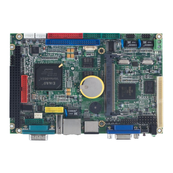
- Page 1 VSX-6126 DM&P Vortex86SX 300MHz 3.5” CPU Module with 4S/3USB/VGA/LCD/LVDS/AUDIO/3LAN/GPIO/CF 128MB DDR2 Onboard User’s Manual (Revision 1.0A)
- Page 2 No part of this manual may be reproduced, copied, translated or transmitted, in whole or in part, in any form or by any means without the prior written permission of the ICOP Technology Inc.. ©Copyright 2007 ICOP Technology Inc.
-
Page 3: Table Of Contents
T a b l e C o n t e n t s T a b l e o f C o n t e n t s ........iii C h a p t e r 1 Introduction……………………………………………1 Packing List............1 Product Description .......... -
Page 4: Chapter 1 Introduction
Package Embedded Vortex86SX CPU All-in-One Board Manual & Drivers CD x 1 RS232 cable x 4 PRINTER cable x1 VSX-6126 IDE cable x 1 USB cable x 1 (USB port x 2 LAN cable x 2 GPIO cable x 1 AUDIO Line x2 YKB for Keyboard &... -
Page 5: Product Description
3.5” controller. The VSX-6126 family of controller is designed as a plug in replacement, with backward compatibility to support legacy software to help extend existing product life cycle without heavy re-engineering. -
Page 6: Specifications
1.3 Specifications Features VSX-6126 DM&P SoC CPU Vortex86SX- 300MHz Real Time Clock with Lithium Battery Backup Cache L1:16K I-Cache, 16K D-Cache BIOS AMI BIOS Bus Interface PC/104 Standard Compliant System Memory 128MB DDR2 onboard Software programmable from 30.5 us to 512 seconds x2... - Page 7 2.00 mm ∅ 44-pin box header for IDE x1 Connectors 2.00 mm ∅ 44-pin box header for LCD x 1 2.00 mm ∅ 26-pin box header for Printer x1 2.00 mm ∅ 20-pin box header for 16-bit GPIO x1 2.00 mm ∅ 16-pin box header for LVDS x 1 2.00 mm ∅...
-
Page 8: Board Dimension
Board Dimension Vortex86SX-6126 Vortex86SX™ 3.5” CPU Module... -
Page 9: Chapter 2 Installation
C h a p t e r 2 Installation Board Outline Vortex86SX-6126 Vortex86SX™ 3.5” CPU Module... -
Page 10: Connectors & Jumpers Location
Connectors & Jumpers Location Connectors Vortex86SX-6126 Vortex86SX™ 3.5” CPU Module... - Page 11 Jumpers & LEDs Vortex86SX-6126 Vortex86SX™ 3.5” CPU Module...
-
Page 12: Connectors & Jumpers Summary
Connectors & Jumpers Summary Summary Table Description Type of Connections Pin nbrs. 44-pin Box Header, 2.0∅ ,22x2 USB 2 USB connector 4-pin USB 0 & USB 1 10-pin Box Header,2.0∅ , 5x2 LAN 1 8-pin RJ45 Connector JTAG 6-pin Wafer, 1.25∅ , 6x1 Reset 2-pin Pin Header, 2,54∅,1x2... - Page 13 LAN 3 8-pin Pin Header, 2.0∅ , 4x2 CF Card Master/Slave Select 3-pin Slide SW LINE-OUT 4-pin Molex Header, 2.0∅, 4x1 MIC-IN 4-pin Molex Header, 2.0∅, 4x1 Compact Flash 50-pin Type I/II CF Connector LAN Link/Active LED (Green) LED-SMD LAN Duplex LED ( Yellow ) LED-SMD LAN Link/Active LED (Green) LED-SMD...
-
Page 14: Pin Assignments & Jumper Settings
Pin Assignments & Jumper Settings J1: IDE (44 Pins) Pin # Signal Name Pin # Signal Name IDERST IDED7 IDED8 IDED6 IDED9 IDED5 IDED10 IDED4 IDED11 IDED3 IDED12 IDED2 IDED13 IDED1 IDED14 IDED0 IDED15 IDEREQ IDEIOW IDEIOR ICHRDY IDEACK IDEINT IDESA1 IDECBLID IDESA0... - Page 15 J7: JTAG Pin # Signal Name Pin # Signal Name J8: RESET Pin # Signal Name Pin # Signal Name Reset J9: PS/2 Keyboard / Mouse Pin # Signal Name Pin # Signal Name KBDATA KBCLK MSDATA MSCLK GGND GGND GGND GGND GGND...
- Page 16 J11: GPIO (Port 0 / 1) Pin # Signal Name Pin # Signal Name GP00 GP10 GP01 GP11 GP02 GP12 GP03 GP13 GP04 GP14 GP05 GP15 GP06 GP16 GP07 GP17 J12: COM2 (RS232 / RS485) Pin # Signal Name Pin # Signal Name DCD2 RXD2 TXD2...
- Page 17 J16: Power Connector (Terminal Block 5.0mm) Pin # Signal Name J17: COM3 Pin # Signal Name Pin # Signal Name DCD3 RXD3 TXD3 DTR3 DSR3 RTS3 CTS3 J18: PRINT Pin # Signal Name Pin # Signal Name STB- ACK- BUSY SLCT AFD- ERR-...
- Page 18 J19: COM4 Pin # Signal Name Pin # Signal Name DCD4 RXD4 TXD4 DTR4 DSR4 RTS4 CTS4 J25: PC104 Connector – 64pin Pin # Signal Name Pin # Signal Name IOCHCHK * RESETDRV IRQ9 DRQ2 -12V +12V IOCHRDY SMEMW * SA19 SMEMR * SA18...
- Page 19 J26: PC104 Connector – 40pin Pin # Signal Name Pin # Signal Name MEMCS16 * SBHE * IOCS16 * SA23 IRQ10 SA22 IRQ11 SA21 IRQ12 SA20 IRQ15 SA19 IRQ14 SA18 DACK0 * SA17 DRQ0 MEMR * DACK5 * MEMW * DRQ5 DACK6 * DRQ6...
- Page 20 J30: VGA Pin # Signal Name Pin # Signal Name R OUT G OUT B OUT DDCDAT HSYNC VSYNC DDCCLK J31: LVDS Pin # Signal Name Pin # Signal Name VCC3 (3.3V) VCC3 (3.3V) RxIN0- RxIN0+ RxIN1- RxIN1+ RxIN2+ RxIN2- CKIN- CKIN+ Vortex86SX-6126...
- Page 21 J32~J38: Display type setup (CRT /LCD) Connector Pin # Signal Name GPIOA GPIOB GPIOC GPIOD GPIOE GPIOF (Please refer to Appendix D, for Display type setup) Vortex86SX-6126 Vortex86SX™ 3.5” CPU Module...
- Page 22 J33: LCD (DVO) Connector Pin # Signal Name Pin # Signal Name VCC3 VCC3 LCLK LHSYNC LVSYNC LBACKL LVDDEN (Please refer to Appendix A, for TFT Flat Panel Data Output) J39: LAN 2 Pin # Signal Name Pin # Signal Name TX+1 TX-1 RX+1...
- Page 23 J40: LAN 3 Pin # Signal Name Pin # Signal Name TX+2 TX-2 RX+2 LED02 LED02+ RX-2 LED12+ LED12 J42: LINE OUT Pin # Signal Name LOUTR LOUTL J43: MIC-IN Pin # Signal Name MICVREF MIC-IN Vortex86SX-6126 Vortex86SX™ 3.5” CPU Module...
-
Page 24: System Mapping
System Mapping Vortex86SX-6126 Vortex86SX™ 3.5” CPU Module... - Page 25 Vortex86SX-6126 Vortex86SX™ 3.5” CPU Module...
- Page 26 Vortex86SX-6126 Vortex86SX™ 3.5” CPU Module...
-
Page 27: Watchdog Timer
Watchdog Timer There are two watchdog timers in Vortex86SX CPU. One is compatible with M6117D watchdog timer and the other is new. The M6117D compatible watchdog timer is called WDT0 and new one is called WDT1. We also provide DOS, Linux and WinCE example for your reference. For more technical support, please visit: http://www.dmp.com.tw/tech or download the PDF file:... -
Page 28: Gpio
GPIO (General Purpose Input / Output) 40 GPIO pins are provided by the Vortex86SX for general usage in the system. All GPIO pins are independent and can be configured as inputs or outputs, with or without pull-up/pull-down resistors. We also offer DOS, Linux and WinCE example for your reference. For more technical support, please visit: http://www.dmp.com.tw/tech or download the PDF file:... -
Page 29: Spi Flash
SPI flash (Serial Peripheral Interface) As SPI Flash Serial Peripheral Interface) offers many benefits including: reduced controller pin count, smaller and simpler PCBs, reduced switching noise, less power consumption, and lower system cost Many of users may consider using a formatted SPI flash to boot for the system or emulate SPI flash as Floppy (A: Driver or B: Driver). -
Page 30: Chapter 3 Driver Installation
C h a p t e r Driver Installation The Vortex86SX processor also use external Display chip ““Volari™ Z9s” which is an ultra low powered graphics chipset with total power consumption at around 1-1.5 W. It is capable in providing VGA display output upto 1600x1200. With DVO interface, developers could easily connect flat Panel to support TFT and LVDS output. -
Page 31: Appendix
Appendix TFT Flat Panel Data Output Vortex86SX-6126 Vortex86SX™ 3.5” CPU Module... -
Page 32: Tft Flat Panel Support List
B.TFT Flat Panel Support List Size Brand Resolution Model No. 5.7” Data image 320x240 FG050701DSSWBG01 5.7” Optrex 320x240 55264GD057J-FW-ABN 5.7” TOSHIBA 320x240 LTA057A343F 5.7” Sharp 320x240 (QVGA / VGA) LQ057Q3DC02 5.7” Kyocera 320x240 (QVGA / VGA) TCG057QV1AC-G10 5.7” 320x240 (QVGA / VGA) PD057VU4 /U5 5.7”... -
Page 33: Lvds Flat Panel Support List
C. LVDS Flat Panel Support Size Brand Resolution Model No. 3.5” 640x480 PD035VL1 6.5” 640x480 G065VN01 8.4” 800x600 G084SN03 10.4” MITSUBISHI 800x600 AA104SG01 10.4” 800x600 G104SN02 10.4” Sharp 800x600 LQ104S1LG61 12.1” MITSUBISHI 800x600 AA121SL03 12.1” 800x600 G121SN01 Vortex86SX-6126 Vortex86SX™ 3.5” CPU Module... -
Page 34: Flat Panel Hardware Setting
D. Flat Panel Hardware Setting: The Vortex86SX-6126 offers the Hardware setting for the various TFT LCD Flat Panels support and please make sure the jumper setting (J32~J38) before you connect the LCD. Display type setup Connector Note: "C" means close; "O" means open Vortex86SX-6126 Vortex86SX™... -
Page 35: Flat Panel Wiring And Lighting
Wiring LCD Cable Please refer to Page 19 (J33: LCD connector) and Page 28~32. Or for more LCD lighting and integration service, please contact our regional sales or mail to info@icop.com.tw you have any questions. Vortex86SX-6126 Vortex86SX™ 3.5” CPU Module... -
Page 36: Tcp/Ip Library For Dos Real Mode
Mity-Mite Serial Server, Web Camera Tiny Server and RSIP Serial Server. DSock is free for All ICOP products using M6117D/Vortex86/Vortex86SX CPU and ICOP also provide the business version of DSock for those customers who are using other x86 CPUs. -
Page 37: Bios Default Setting
G. BIOS Default setting If the system cannot be booted after BIOS changes are made, Please follow below procedures in order to restore the CMOS as default setting. Press “End” Key, when the power on Press <Del> to enter the AMI BIOS setup Press “F9”... -
Page 38: Warranty
Warranty This product is warranted to be in good working order for a period of one year from the date of purchase. Should this product fail to be in good working order at any time during this period, we will, at our option, replace or repair it at no additional charge except as set forth in the following terms.
Need help?
Do you have a question about the VSX-6126 and is the answer not in the manual?
Questions and answers