Table of Contents
Advertisement
Quick Links
Introduction
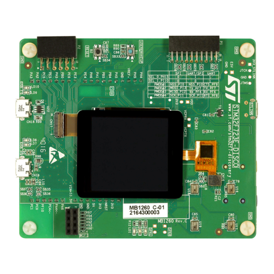
The 32F723EDISCOVERY Discovery kit is a complete demonstration and development
platform for the STMicroelectronics ARM
microcontroller. It features the following interfaces: three I
multiplexed simplex I
UARTs peripherals, one CAN bus, three 12-bit ADCs, two 12-bit DACs, two SAIs, internal
256 Kbytes of SRAM, 512 Kbytes of Flash memory, one USB OTG HS internal PHY, USB
OTG FS and SWD debugging support. This 32F723EDISCOVERY Discovery kit offers
everything required for users to get started quickly and develop applications easily.
The full range of hardware features on the board helps users to evaluate almost all
peripherals (USB OTG HS, USB OTG FS, USART, SAI Audio DAC stereo with audio jack
input and output, ST-MEMS digital microphones, external PSRAM, Quad-SPI Flash memory,
LCD with capacitive multi-touch panel and others) and develop applications. Arduino
V3, PMOD and STMod+ connectors allow easy connection of extension shields or
daughterboards for specific applications.
The integrated ST-LINK/V2-1 provides an embedded in-circuit debugger and programmer for
the STM32.
The 32F723EDISCOVERY Discovery kit comes with the STM32 comprehensive software
HAL library together with various packaged software examples.
Figure 1. 32F723EDISCOVERY (top view)
1. Pictures are not contractual.
February 2017
Discovery kit with STM32F723IE MCU
®
2
S, 2xSDMMC, FMC, Quad-SPI. It also features four USARTs and four
Figure 2. 32F723EDISCOVERY (bottom view)
DocID029990 Rev 1
Cortex
®
-M7 core-based STM32F723IEK6
2
Cs, five SPIs with three
UM2140
User manual
™
Uno
www.st.com
1/59
1
Advertisement
Table of Contents

Related Manuals for ST UM2140


Summary of Contents for ST UM2140
-
Page 1: Figure 1. 32F723Ediscovery (Top View)
The full range of hardware features on the board helps users to evaluate almost all peripherals (USB OTG HS, USB OTG FS, USART, SAI Audio DAC stereo with audio jack input and output, ST-MEMS digital microphones, external PSRAM, Quad-SPI Flash memory, ™... -
Page 2: Table Of Contents
Embedded ST-LINK/V2-1 ........14... - Page 3 Control Touch Panel (CTP) Frida connector ..... . 30 ST-LINK/V2-1 USB Micro-B connector CN1 ..... . 31 8.10...
- Page 4 Contents UM2140 Appendix E Federal Communications Commission (FCC) and Industry Canada (IC) Compliance Statements... . . 56 FCC Compliance Statement ........56 E.1.1...
- Page 5 UM2140 List of tables List of tables Table 1. Ordering Information ............9 Table 2.
- Page 6 ST-LINK/V2-1 with support of SWD ........
-
Page 7: Features
• STM32F723IEK6 microcontroller featuring 512 Kbytes of Flash memory and 256 Kbytes of SRAM, in UFBGA176 package • On-board ST-LINK/V2-1 debugger • USB ST-LINK functions: virtual COM port, mass storage and debug port • TFT LCD 240x240 pixels with touch panel • SAI audio codec •... -
Page 8: Product Marking
Any consequences deriving from such usage will not be at ST charge. In no event, ST will be liable for any customer usage of these engineering sample tools as reference design or in production. -
Page 9: Demonstration Software
Demonstration software The demonstration software is preloaded in the STM32F723IEK6 Flash memory. The latest versions of the demonstration source code and associated documentation can be downloaded from the www.st.com/stm32f7-Discovery webpage. Ordering information To order the 32F723EDISCOVERY Discovery kit, refer to Table Table 1. -
Page 10: Hardware Layout And Configuration
3) illustrates the connection between STM32F723IEK6 and peripherals (PSRAM, Quad-SPI Flash memory, LCD connector, USB OTG HS and FS connectors, USART, Audio, Arduino Uno V3, PMOD and STMod+ shields and embedded ST-LINK). Figure 4 Figure 5 help users to locate these features on the 32F723EDISCOVERY board. -
Page 11: The 32F723Ediscovery Discovery Kit Layout
UM2140 Hardware layout and configuration The 32F723EDISCOVERY Discovery kit layout Figure 4. 32F723EDISCOVERY top layout Control Four ST MEMS Touch Panel microphones on onnector DFSDM inputs (FRIDA) STMod+ connector TFT LCD 240x240 pixels (FRIDA) User LED Arduino LED WAKE-UP button... -
Page 12: Figure 5. 32F723Ediscovery Bottom Layout
Hardware layout and configuration UM2140 Figure 5. 32F723EDISCOVERY bottom layout STM32F103CBT6 ST890CDR Output audio ST-LINK power limiter ST-LINK ST LINK/V2-1 line jack COM LED Fault LED with Micro-B Power Input audio connector JTAG line jack 5V external 512-Mbit power Quad-SPI... -
Page 13: The 32F723Ediscovery Discovery Kit Mechanical Drawing
UM2140 Hardware layout and configuration The 32F723EDISCOVERY Discovery kit mechanical drawing Figure 6. 32F723EDISCOVERY mechanical drawing 1. The digital microphones marked in orange (U16, U17, U18 and U19) are placed on the bottom side of the board. DocID029990 Rev 1... -
Page 14: Embedded St-Link/V2-1
Before connecting the 32F723EDISCOVERY board to a Windows 7, Windows 8 or ® Windows XP PC via USB, a driver for ST-LINK/V2-1 must be installed. It can be downloaded from the www.st.com website. In case the 32F723EDISCOVERY board is connected to the PC before installing the driver, the PC device manager may report some 32F723EDISCOVERY board interfaces as “Unknown”. -
Page 15: St-Link/V2-1 Firmware Upgrade
The ST-LINK/V2-1 embeds a firmware upgrade mechanism for in-situ upgrade through the USB port. As the firmware may evolve during the life time of the ST-LINK/V2-1 product (for example a new functionality, bug fixes, support for new microcontroller families), it is recommended to visit the www.st.com... -
Page 16: Supplying The Board Through A Charger Connected To St-Link
The LED LD2 is lit when the 32F723EDISCOVERY board is powered by the 5 V correctly. Caution: Do not connect a PC to ST-LINK (CN1) when R5 is soldered. The PC may be damaged or the board not powered correctly. -
Page 17: Supplying The Board From E5V (Cn3 Or Cn12)
UM2140 Hardware layout and configuration Figure 9. CN8 (USB_STLINK) 7.4.3 Supplying the board from E5V (CN3 or CN12) Figure 10. CN8 (External 5V supply) From E5V: 5V DC power adapter connected to CN3 In this case, the 32F723EDISCOVERY board must be powered by a power supply unit or by... -
Page 18: Supplying The Board From An External Power Supply Through Usb Hs
Hardware layout and configuration UM2140 7.4.4 Supplying the board from an external power supply through USB HS A 5 V DC external power supply is connected to USB OTG HS Micro-AB connector CN19 (5 V power source on silkscreen “USB_HS”, refer to Figure 11). -
Page 19: Clock Sources
If this order is not respected, the 32F723EDISCOVERY Discovery board may be powered by first from ST-LINK and the following risks may be encountered: If more than 500 mA current is needed by the board, the PC may be damaged or current can be limited by PC. -
Page 20: Usb Otg Hs
USB device. The red LED LD7 is lit when an overcurrent occurs. Note:1 When the 32F723EDISCOVERY board is powered by the ST-LINK then the OTG function can provide up to 100 mA. Note:2 When the 32F723EDISCOVERY board is powered by an external power supply then the OTG function can provide more than 100 mA, according to the external power supply capability. -
Page 21: Psram Memory
The serial interface USART6 is directly available as a virtual COM port of the PC connected to the ST-LINK/V2-1 USB connector CN1. The virtual COM port settings are configured as: 115200 b/s, 8 bits data, no parity, 1 stop bit, no flow control. -
Page 22: Table 3. Control Port Assignment
Hardware layout and configuration UM2140 Table 3. Control port assignment Reference Color Name Comment BLUE USER Alternate function Wake-up BLACK RESET BLUE ARDUINO 5 V Power Fault Power Current upper than 625 mA RED/GREEN STLINK COM Green when communication USER1... -
Page 23: Connectors
UM2140 Connectors Connectors Wi-Fi ESP-01 compatible connector Figure 13. Wi-Fi connector CN14 (front view) Table 4. Wi-Fi extension connector CN14 Pin number Wi-Fi description WIFI_RX 3.3 V GPIO0 WIFI-RST GPIO2 CH_PD WIFI_TX Arduino Uno V3 compatible connectors CN11, CN12, CN13 and CN15 are female connectors compatible with Arduino Uno V3 standard. -
Page 24: Pmod And Stmod+ Connectors P2 And P1
Connectors UM2140 Table 5. GPIO assignment for Arduino pins Name Pin number Name CN11.10 SCL2 CN11.9 SDA2 CN11.8 VREF+ CN11.7 CN12.1 CN11.6 SCK1 3.3 V CN12.2 CN11.5 MISO1 NRST CN12.3 CN11.4 MOSI1 3.3 V CN12.4 CN11.3 NSS1 CN12.5 CN11.2 TIM12_CH1 CN12.6... -
Page 25: Pmod Connector P2
UM2140 Connectors 8.3.1 PMOD connector P2 PMOD connector is 2x6 pins with 2.54 mm pitch and right-angle female connector. Samtec SSW-106-02-F-D-RA is selected for PMOD connector (second source is available: ATOM FH254206C-1600). Figure 14. PMOD: Samtec SSW connector (P2) Table 6. GPIO assignment for PMOD pins... -
Page 26: Stmod+ Connector P1
Connectors UM2140 8.3.2 STMod+ connector P1 STMod+ connector is 2x10 pins with 2.0 mm pitch and right angle female connector. Samtec SQT-110-01-F-D-RA is selected for STMod+ connector (second source: ATOM FH200210C-12000). Figure 15. STMod+: Samtec SQT connector (P1) Table 8. GPIO assignment for STmod+ pins... -
Page 27: Tag Connector Cn9
TAG connector CN9 TAG connector is a 10-pin footprint supporting SWD mode, which shares same signals with ST-LINK: PA13 (JTMS / SWDIO), PA14 (JTCLK / SWCLK), PB3 (JTDO / SWO), PB4 (NRST). TC2050-IDC-NL cable is used to link ST-LINK and TAG connector, so users can easily program and debug the STM32 without using any extra accessory. -
Page 28: Usb Otg Hs Micro-Ab Connector
Connectors UM2140 USB OTG HS Micro-AB connector Figure 17. USB OTG HS Micro-AB connector CN19 (front view) Table 10. USB OTG HS Micro-AB connector CN19 Pin number Description Pin number Description Note: STMPS U13 is providing V . It is active high, controlled by PH12. Overcurrent is sent to PH10 interrupt. -
Page 29: Lcd Frida Connector
UM2140 Connectors LCD Frida connector Figure 19. LCD Frida connector (Hirose FH26-29S-0.3SHW) CN17 (front view) Table 12. Pin description of the LCD Frida connector CN17 Pin number Description Pin number Description connection connection FMARK PC8 (TE INT) DB15 FMC_D15 DB14... -
Page 30: Control Touch Panel (Ctp) Frida Connector
Connectors UM2140 Control Touch Panel (CTP) Frida connector Figure 20. CTP connector ((Hirose DF37NB-10DS-0.4V (5x)) CN16 (front view) Table 13. Pin description of the CTP connector CN16 Pin number Description RESET IOVCC 30/59 DocID029990 Rev 1... -
Page 31: St-Link/V2-1 Usb Micro-B Connector Cn1
UM2140 Connectors ST-LINK/V2-1 USB Micro-B connector CN1 The USB connector CN1 is used to connect embedded ST-LINK/V2-1 to PC for programming and debugging of STM32F723IEK6 microcontroller. Figure 21. USB Micro-B connector CN1 (front view) Table 14. USB Micro-B connector CN1... -
Page 32: Audio Line Output (Green Jack) Connector
Connectors UM2140 8.11.1 Audio line output (green jack) connector A 3.5 mm stereo audio green jack output CN5 is available to support the headphone (see Figure 22). Table 15. Audio line output connector CN5 Pin number Description Right Left 8.11.2 Audio line input (blue jack) connector A 3.5 mm stereo audio blue jack input CN4 is available to support the audio line input (see... -
Page 33: Appendix A 32F723Ediscovery Discovery Board I/O Assignment
UM2140 32F723EDISCOVERY Discovery board I/O assignment Appendix A 32F723EDISCOVERY Discovery board I/O assignment Table 17. I/O assignment Function Label number GPIO_Output ARD_D7_GPIO QUADSPI_BK1_IO2 FMC_NBL1 FMC_NBL0 I2C1_SCL SPI1_MOSI ARD_D11_TIM3_CH2_SPI1_MOSI PG14 GPIO_Output WIFI_RST PG13 GPIO_Output WIFI_GPIO_0 SPI1_MISO ARD_D12_SPI1_MISO SYS_JTDO-SWO FMC_NE1 PC12 UART5_TX... - Page 34 32F723EDISCOVERY Discovery board I/O assignment UM2140 Table 17. I/O assignment (continued) Function Label number SAI2_SCK_A FMC_NE2 FMC_NWE FMC_D3 GPIO_Output PMOD_SPI2_MOSI GPIO_Output PMOD_SPI2_MISO PA11 USB_OTG_FS_DM GPIO_EXTI9 CTP_INT SAI2_MCLK_A FMC_NOE GPIO_Output WIFI_CH_PD UART5_RX UART_RXD_WIFI_TX PH15 GPIO_Output PMOD_SEL_0 SPI2_SCK PMOD_SPI2_SCK PA10 GPIO_Output USB_OTG_FS_ID...
- Page 35 UM2140 32F723EDISCOVERY Discovery board I/O assignment Table 17. I/O assignment (continued) Function Label number GPIO_Output USB_OTGFS_PPWR_EN USART6_TX FMC_A3 FMC_A4 I2C2_SDA ARD_D14_STMOD+_I2C2_SDA UART7_TX PMOD_UART7_TXD UART7_RX PMOD_UART7_RXD FMC_A5 PH12 GPIO_Output USB_OTGHS_PPWR_EN FMC_A15 FMC_A14 FMC_A13 PF10 ADC3_IN8 ARD_A3_ADC3_IN8 UART7_CTS PMOD_UART7_CTS UART7_RTS PMOD_UART7_RTS PH11...
- Page 36 32F723EDISCOVERY Discovery board I/O assignment UM2140 Table 17. I/O assignment (continued) Function Label number PF13 FMC_A7 FMC_A10 PE13 FMC_D10 GPIO_Output LCD_RST PD12 FMC_A17 PD11 FMC_A16 PD10 FMC_D15 USART2_TX ARD_D1_USART2_TX ADC2_IN6 SPI1_SCK ARD_D13_SPI1_SCK GPIO_Output ARD_D2_GPIO PF12 FMC_A6 PF15 FMC_A9 FMC_D5 FMC_D6...
- Page 37 UM2140 32F723EDISCOVERY Discovery board I/O assignment Table 17. I/O assignment (continued) Function Label number PB14 USB_OTG_HS_DM PB15 USB_OTG_HS_DP 1. Shared between Arduino and STMod+. 2. Exclusive use: Arduino or STMod+. DocID029990 Rev 1 37/59...
-
Page 38: Appendix B Electrical Schematics
This section provides design schematics of the features for the 32F723EDISCOVERY Discovery board and Fanout boards: • MB1260 (32F723EDISCOVERY Discovery board) – 32F723EDISCOVERY Discovery board interconnexion (Figure – ST-LINK/V2-1 with support of SWD only (Figure – STM32F723IEK6 connections (Figure – Audio codec WOLFSON and Audio connectors (Figure –... -
Page 39: Figure 23. 32F723Ediscovery Discovery Board Interconnections
Figure 23. 32F723EDISCOVERY Discovery board interconnections U_USB_OTG_FS USB_OTG_FS.SchDoc U_LCD_FRIDA U_STM32F7 LCD_FRIDA.SchDoc STM32F7.SchDoc USB_OTGFS_OVCR USB_OTGFS_OVCR USB_OTGFS_PPWR_EN USB_OTGFS_PPWR_EN LCD_PSRAM_NWE LCD_PSRAM_NWE USB_OTGFS_VBUS USB_OTGFS_VBUS LCD_PSRAM_NOE LCD_PSRAM_NOE USB_OTGFS_N USB_OTGFS_N LCD_NE LCD_NE USB_OTGFS_P USB_OTGFS_P LCD-RS_A0 LCD-RS_A0 USB_OTGFS_ID USB_OTGFS_ID LCD_PSRAM_D[0..15] LCD_PSRAM_D[0..15] LCD_TE_INT LCD_TE_INT LCD_BL LCD_BL PSRAM Data, NWE U_USB_OTG_HS LCD_RST LCD_RST... -
Page 40: Figure 24. St-Link/V2-1 With Support Of Swd
Figure 24. ST-LINK/V2-1 with support of SWD 3V3_ST_LINK SB11 SYS_STLINK_JTMS PA13 T_JTMS SYS_STLINK_JTMS SB12 SYS_STLINK_JTCK PA14 T_JTCK SYS_STLINK_JTCK SB13 SYS_STLINK_JTDO-SWO T_SWO SYS_STLINK_JTDO-SWO LED_STLINK T_NRST SB10 NRST NRST 100nF 100nF 100nF 100nF 3V3_ST_LINK _Green SWCLK SWDIO LD_BICOLOR_CMS BAT60JFILM STM_JTCK STM_JTMS 100K... -
Page 41: Figure 25. Stm32F723Iek6 Connections
Figure 25. STM32F723IEK6 connections QSPI_D3 USB_OTGHS_OVCR PSRAM_A[0..17] QSPI_D3 USB_OTGHS_OVCR PSRAM_A[0..17] SAI2_SCK_A QSPI_D2 USB_OTGHS_PPWR_EN LCD_PSRAM_D[0..15] ARD_A[0..5] STMOD+_TIM2_CH1 SAI2_SCK_A QSPI_D2 USB_OTGHS_PPWR_EN LCD_PSRAM_D[0..15] ARD_A[0..5] STMOD+_TIM2_CH1 TP11 SAI2_FS_A QSPI_D1 USB_OTGHS_VBUS LCD_PSRAM_NWE ARD_D[0..15] STMOD+_SPI2_MISOs SAI2_FS_A QSPI_D1 USB_OTGHS_VBUS LCD_PSRAM_NWE ARD_D[0..15] STMOD+_SPI2_MISOs TP12 SAI2_SD_A QSPI_D0 USB_OTGHS_N LCD_PSRAM_NOE STMOD+_SPI2_MOSIs SAI2_SD_A QSPI_D0... -
Page 42: Figure 26. Audio Codec Wolfson And Audio Connectors
Figure 26. Audio codec WOLFSON and Audio connectors SAI2_SCK_A SAI2_SCK_A SAI2_FS_A SAI2_FS_A SAI2_SD_A SAI2_SD_A WM8994 I2C Address : 0011 0100 SAI2_SD_B SAI2_SD_B LDO1VDD AGND SAI2_INT SAI2_INT AVDD1 AGND SAI2_I2C1_SDA SAI2_I2C1_SDA SPKVDD1 AGND SAI2_I2C1_SCL SAI2_I2C1_SCL SPKVDD2 SPKGND1 SAI2_MCLK_A SAI2_MCLK_A AVDD2 SPKGND2 CPVDD CPGND DCVDD... - Page 43 Figure 27. PSRAM Impedance Constraint [Min = 40.00 Max = 60.00 Matched Net Lengths [Tolerance = 200mil] PSRAM Data, NWE & NOE PSRAM_D shared with LCD LCD_PSRAM_D[0..15] LCD_PSRAM_D[0..15] PSRAM_A[0..17] PSRAM_A[0..17] PSRAM_A Matched Net Lengths [Tolerance = 200mil] LCD_PSRAM_D15 I/O15 Impedance Constraint [Min = 40.00 Max = 60.00 LCD_PSRAM_D14 I/O14...
-
Page 44: Figure 28. Quad-Spi Flash Memory (Micron)
Figure 28. Quad-SPI Flash memory (MICRON) Quad SPI Flash Memory Matched Net Lengths [Tolerance = 100mil] QSPI QSPI QSPI_NCS QSPI_NCS QSPI_CLK QSPI QSPI_CLK SCLK SCLK QSPI QSPI_D0 QSPI QSPI_D0 SIO0/SI SIO0/SI QSPI_D1 QSPI 100nF QSPI_D1 SIO1/SO SIO1/SO QSPI_D2 QSPI_D2 SIO2/WP# SIO2/WP# QSPI_D3 QSPI_D3... -
Page 45: Figure 29. Arduino Uno V3 Connectors
Figure 29. Arduino Uno V3 connectors Arduino UNO connector ARD_A[0..5] ARD_A[0..5] ARD_D[0..15] SB14 VREF+ ARD_D[0..15] 680_1%_0402 LED blue CN11 PH4 (*) ARD_D15 SCL/D15 PH5 (*) ARD_D14 Fitted: NO SDA/D14 CN12 AVDD ARD_D13 SPI1_SCK IOREF SCK/D13 NRST ARD_D12 SPI1_MISO NRST MISO/D12 NRST ARD_D11 TIM3_CH2, SPI1_MOSI... -
Page 46: Figure 30. Usb Otg Hs Phy With Micro-Ab Connector
Figure 30. USB OTG HS PHY with Micro-AB connector PH10 USB_OTGHS_OVCR USB_OTGHS_OVCR LED red FAULT LED green 4.7uF VBUS OK PH12 USB_OTGHS_PPWR_EN USB_OTGHS_PPWR_EN Active high STMPS2151STR 9013-SOT23 PB13 USB_OTGHS_VBUS 100K USB_OTGHS_VBUS 5V_USB_HS 0_5%_0805 Impedance Constraint [Min = 85.00 Max = 95.00 ] CN19 Matched Net Lengths [Tolerance = 0.2mm] Vbus... -
Page 47: Figure 31. Usb Otg Fs
Figure 31. USB OTG FS PB10 USB_OTGFS_OVCR USB_OTGFS_OVCR 5V_USB_FS LD10 LED red CN18 FAULT VBUS USB_OTGFS_PPWR_EN USB_OTGFS_PPWR_EN Active low Open Drain STMPS2141STR 4.7uF Shield Shield USB_OTGFS_VBUS USB_OTGFS_VBUS Shield Shield Impedance Constraint [Min = 85.00 Max = 95.00 ] Matched Net Lengths [Tolerance = 0.2mm] 475900001 PA11 USB_OTGFS_N... -
Page 48: Figure 32. Lcd Frida
Figure 32. LCD Frida 240x240 pixels TFT LCD LCD FRIDA Top side: layout of CN12 FRD154BP2902-CTP pixel (0,0) * PSRAM Data, NWE & NOE shared CN17 LCD_TE_INT with LCD FMARK LCD_PSRAM_D15 LCD_PSRAM_D14 DB15 DB14 LCD_PSRAM_D[0..15] LCD_PSRAM_D13 LCD_PSRAM_D12 LCD_PSRAM_D[0..15] DB13 DB12 LCD_NE LCD FRIDA FRD154BP2901 LCD_PSRAM_D11... -
Page 49: Figure 33. Wi-Fi, Leds And Push-Buttons
Figure 33. Wi-Fi, LEDs and push-buttons WIFI_TX WIFI_TX WIFI_RX PMOD WIFI with ESP8266 WIFI_RX WIFI_RST WIFI_RST R102 WIFI_GPIO_0 WIFI_GPIO_0 WIFI_GPIO_2 WIFI_GPIO_2 WIFI_CH_PD WIFI_CH_PD PH15 PMOD_UART7_TXD PMOD_SEL_0 PMOD_UART7_TXD 1-2SEL PMOD_SEL_0 PMOD_SPI2_MOSI PMOD_SPI2_MOSI MOSIp/TX PMOD#2 PMOD_UART7_RXD PMOD_UART7_RXD MISOp/RX PMOD_SPI2_MISO PMOD#3 PMOD_SPI2_MISO PI10 PMOD_UART7_CTS PMOD_SEL_1 CN14... -
Page 50: Figure 34. Fanout Board
Figure 34. Fanout board PMOD+ Grove connector PMOD#1-NSS/CTS PMOD#1 PMOD#11 PMOD#11-INT PMOD#2-MOSIp/TX PMOD#2 PMOD#12 PMOD#12-RST BSN20[N/A] 4K7[N/A] PMOD#3-MISOp/RX PMOD#3 PMOD#13 PMOD#13-ADC 4K7[N/A] PMOD#4-SCK/RTS PMOD#4 PMOD#14 PMOD#14-PWM PMOD#7 I2C_SCL I2C_SCL I2C_SDA PMOD#7-SCL PMOD#7 PMOD#17 PMOD#17-DF-D3 BSN20[N/A] PMOD#8-MOSIs PMOD#8 PMOD#18 PMOD#18-DF-CK3 PMOD#9-MISOs PMOD#9 PMOD#19 PMOD#19-DF-D7... -
Page 51: Appendix C Pmod And Stmod+ Schematic Table
UM2140 PMOD and STMod+ schematic table Appendix C PMOD and STMod+ schematic table Table 18 gives the description of the signals available on the STMod+ connector. It also shows which signal is shared with other board connectors (such as PMOD or Arduino Uno V3). -
Page 52: Table 18. Stmod+ Connector Signals
Table 18. STMod+ connector signals STMod+ PMOD Some other AF Basic Pin number Basic Some other AF PMOD MOSI5/[ADC3.7]/T14.1 CTS7 PI10=1 PB11 SDA2/RX3/T2.4 T5.4 NSS2 PI10=0 SCK5/[ADC3.5]/T11.1 PH15=1 PF11 MOSI5 MOSI T8.8ETR MOSI2p PH15=0 NSS5/[ADC3.4]/T10.1 PH15=1 NSS1/NSS3/CK2/[ADC2.4]/ GPIO ADC/DAC [DACOUT1.1] (PG12) MISO T8.4... -
Page 53: Appendix D Fanout Board
UM2140 Fanout board Appendix D Fanout board The Fanout board (see Table 35) comes with the 32F723EDISCOVERY Discovery board. It is connected to STMOD+ connector (P1) and it provides access to: • MikroElektronika Click board compatible connectors (CN10 and CN11: two 1x8-pin female connectors) •... -
Page 54: Mikroelektronika Mikrobus™ Compatible Connector (Fanout Cn10 And Cn11)
Fanout board UM2140 MikroElektronika mikroBUS™ compatible connector (Fanout CN10 and CN11) The mikroBUS™ compatible connector is 2.54" pitch with a pair of 1x8-pin female connectors. Table 19 below shows the definition of the pins. Table 19. Description of the mikroBUS™ connector pins... -
Page 55: Compatible Connectors For The Grove Boards
UM2140 Fanout board Compatible connectors for the Grove boards The two connectors of the Grove board are 2.54 pitch with 1x4-pin male connectors, the part number is 1125S-SMT-4P. D.3.1 Compatible connector for I C Grove boards (Fanout CN3) The CN3 connector is compatible with Grove- Barometer sensor (BMP180) and Grove-LCD RGB Backlight boards using cable for connection. - Page 56 Federal Communications Commission (FCC) and Industry Canada (IC) Compliance Statements Appendix E Federal Communications Commission (FCC) and Industry Canada (IC) Compliance Statements FCC Compliance Statement E.1.1 Part 15.19 This device complies with Part 15 of the FCC Rules. Operation is subject to the following two conditions: (1) this device may not cause harmful interference, and (2) this device must accept any interference received, including interference that may cause undesired operation.
- Page 57 UM2140 CISPR32 Appendix F CISPR32 Warning Warning: This device is compliant with Class A of CISPR32. In a residential environment, this equipment may cause radio interference. DocID029990 Rev 1 57/59...
-
Page 58: Table 23. Document Revision History
Revision history UM2140 Revision history Table 23. Document revision history Date Revision Changes 15-Feb-2017 Initial release 58/59 DocID029990 Rev 1... - Page 59 ST products and/or to this document at any time without notice. Purchasers should obtain the latest relevant information on ST products before placing orders. ST products are sold pursuant to ST’s terms and conditions of sale in place at the time of order acknowledgement.
Need help?
Do you have a question about the UM2140 and is the answer not in the manual?
Questions and answers