
Related Manuals for Renesas DA9061-63


Summary of Contents for Renesas DA9061-63
-
Page 1: Abstract
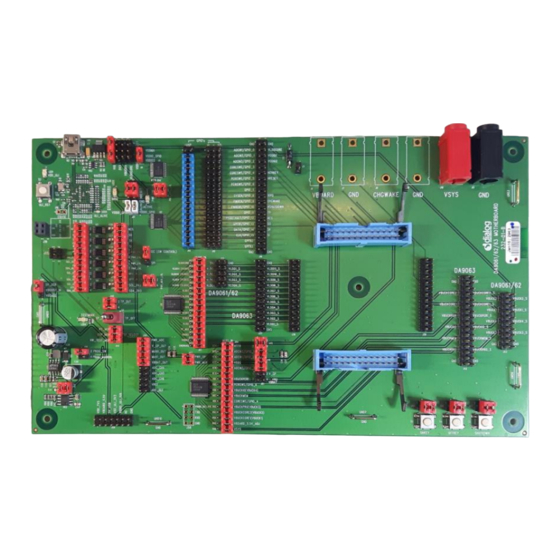
User Manual DA9061-63 Motherboard UM-PM-012 Abstract Explains the setup and operation of the DA9061, DA9062, and DA9063 motherboard. -
Page 2: Table Of Contents
Figure 10: TP Select, PCB ........................12 Figure 11: TP Select, Schematic ......................12 Figure 12: MUX1 ..........................13 Figure 13: MUX2 ..........................13 Figure 14: I C Level Shifter ......................... 13 User Manual Revision 3.0 25-Feb-2022 2 of 15 © 2022 Renesas Electronics... -
Page 3: Terms And Definitions
UM-PM-012 DA9061-63 Motherboard Terms and Definitions Device Under Test Graphical User Interface PMIC Power Management IC USB Lab IO Interface Chip (Atmel) User Manual Revision 3.0 25-Feb-2022 3 of 15 © 2022 Renesas Electronics... -
Page 4: Introduction
(BOOST, LDO) reducing the need for external equipment. Notes and limitations: ● The schematic of the motherboard is delivered with the hardware. Gerber data for the board are available on request. User Manual Revision 3.0 25-Feb-2022 4 of 15 © 2022 Renesas Electronics... -
Page 5: Links
Connects SCLK and MOSI to level shifter J234 To DUT To DUT Connects SK and SI to level shifter Position 1-3 Connects supply for I C level shifter (ULI side) To VDDIO_ULI_1V8 User Manual Revision 3.0 25-Feb-2022 5 of 15 © 2022 Renesas Electronics... - Page 6 Connects VDD_7V5 to LDO To MUX 2 Connects signal rails to MUX 2 Position 1-3 Connect USB interface to NONKEY To NONKEY Position 2-4 Connect pull-up to NONKEY User Manual Revision 3.0 25-Feb-2022 6 of 15 © 2022 Renesas Electronics...
-
Page 7: Motherboard Features
If used in this way, the other links which also control these pins should be removed to avoid logic or voltage clash. User Manual Revision 3.0 25-Feb-2022 7 of 15 © 2022 Renesas Electronics... -
Page 8: Pu/Pd Of Io Signals And Connection To Usb
Place the jumpers in J15 on the left side to connect VDDIO_GPIO via 100 kΩ pull-up resistors, on the right side to connect ground via 100 kΩ pull-down resistors, or leave it open for external connections (see Figure Figure 4: PU/PD and USB Connections User Manual Revision 3.0 25-Feb-2022 8 of 15 © 2022 Renesas Electronics... -
Page 9: Voltage Outputs From Dut
Each pin is connected separately to the regulator output, to a point closest to the device pin. If required, a suitable connector can bring these signals to the system board for integrated development. Figure 6: LDO Connectors User Manual Revision 3.0 25-Feb-2022 9 of 15 © 2022 Renesas Electronics... -
Page 10: Bucks
VBUCKIO (VBUCK4), VLDOCORE, external 3.3 V or external 1.8 V. External voltages are supplied by the USB via external LDOs. VDDIO1/2 can be selected by J2/J3 and VDDIO_GPIO can be selected through VDDIO1/2 via J4. User Manual Revision 3.0 25-Feb-2022 10 of 15 © 2022 Renesas Electronics... -
Page 11: Test Pin (Tp), Pc Mode And Otp Programming Mode
7.5 V activates the OTP programming mode or 0 V to select normal operation mode. In PC mode, register settings are loaded from a file through the software interface. User Manual Revision 3.0 25-Feb-2022 11 of 15 © 2022 Renesas Electronics... -
Page 12: On-Board Multiplexer And Adc
In some cases (such as quiescent current measurements) the input channels might need to be disconnected from the MUX. This can be done by removing the jumper links on J41 and J54. User Manual Revision 3.0 25-Feb-2022 12 of 15 © 2022 Renesas Electronics... -
Page 13: I 2 C Interface
NOTE When using the GUI to select a mode, the Power Commander switch must be in the left-hand position. User Manual Revision 3.0 25-Feb-2022 13 of 15 © 2022 Renesas Electronics... -
Page 14: Revision History
DA9061-63 Motherboard Revision History Revision Date Description 12-Jan-2015 Initial version 06-Jan-2016 Changed references to Smartcanvas GUI. Typographical edits. 25-Feb-2022 File was rebranded with new logo, copyright and disclaimer User Manual Revision 3.0 25-Feb-2022 14 of 15 © 2022 Renesas Electronics... - Page 15 Dialog Semiconductor’s suppliers certify that its products are in compliance with the requirements of Directive 2011/65/EU of the European Parliament on the restriction of the use of certain hazardous substances in electrical and electronic equipment. RoHS certificates from our suppliers are available on request. User Manual Revision 3.0 25-Feb-2022 15 of 15 © 2022 Renesas Electronics...
- Page 16 Renesas' products are provided only subject to Renesas' Terms and Conditions of Sale or other applicable terms agreed to in writing. No use of any Renesas resources expands or otherwise alters any applicable warranties or warranty disclaimers for these products.
Need help?
Do you have a question about the DA9061-63 and is the answer not in the manual?
Questions and answers