
Related Manuals for National Semiconductor LMX2531LQ3010E


Summary of Contents for National Semiconductor LMX2531LQ3010E
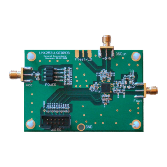
- Page 1 LMX2531LQ3010E Evaluation Board Operating Instructions National Semiconductor Corporation Timing Devices Business Group 10333 North Meridian Suite 400 Indianapolis, IN 46290 LMX25313010EVAL Instructions Rev 6.24.2009...
-
Page 2: Table Of Contents
L M X 2 5 3 1 L Q 3 0 1 0 E E V A L U A T I O N B O A R D O P E R A T I N G I N S T R U C T I O N S Table of Contents Table of Contents ........................ -
Page 3: Loop Filter
10 MHz. • Set up the CodeLoader software. Select the proper part from the menu as Select Part->PLL+VCO->LMX2531LQ3010E Select the proper mode from the Mode menu. Load the part by pressing Ctrl+L or selecting Keyboard Controls->Load Device from the menu. -
Page 4: Troubleshooting
L M X 2 5 3 1 L Q 3 0 1 0 E E V A L U A T I O N B O A R D O P E R A T I N G I N S T R U C T I O N S Troubleshooting Software does not communicate with the evaluation boards LPT or USB Mode... -
Page 5: Far-Out Phase Noise Is Worse Than Evaluation Board Instructions Show
L M X 2 5 3 1 L Q 3 0 1 0 E E V A L U A T I O N B O A R D O P E R A T I N G I N S T R U C T I O N S Far-out Phase noise is worse than evaluation board instructions show •... -
Page 6: Phase Noise
L M X 2 5 3 1 L Q 3 0 1 0 E E V A L U A T I O N B O A R D O P E R A T I N G I N S T R U C T I O N S Phase Noise... -
Page 7: Free-Running Vco Phase Noise (Internal Divide By 2 Disabled)
L M X 2 5 3 1 L Q 3 0 1 0 E E V A L U A T I O N B O A R D O P E R A T I N G I N S T R U C T I O N S Free-Running VCO Phase Noise (Internal Divide by 2 Disabled) The plots to the left show the true phase noise capability of the VCO. -
Page 8: Free-Running Vco Phase Noise (Internal Divide By 2 Enabled)
L M X 2 5 3 1 L Q 3 0 1 0 E E V A L U A T I O N B O A R D O P E R A T I N G I N S T R U C T I O N S Free-Running VCO Phase Noise (Internal Divide by 2 Enabled) The plots to the left show the true phase noise capability of the VCO. -
Page 9: Fractional Spurs (Internal Divide By 2 Disabled)
L M X 2 5 3 1 L Q 3 0 1 0 E E V A L U A T I O N B O A R D O P E R A T I N G I N S T R U C T I O N S Fractional Spurs (Internal Divide by 2 Disabled) The -58.9 dBc fractional spur at 250 kHz offset is at a worst case frequency of 2910.25 MHz. -
Page 10: Fractional Spurs (Internal Divide By 2 Enabled)
L M X 2 5 3 1 L Q 3 0 1 0 E E V A L U A T I O N B O A R D O P E R A T I N G I N S T R U C T I O N S Fractional Spurs (Internal Divide by 2 Enabled) The -65.2 dBc fractional spur at 250 kHz offset is at a worst case frequency of 1455.125 MHz. -
Page 11: Integer Spurs (Internal Divide By 2 Disabled)
L M X 2 5 3 1 L Q 3 0 1 0 E E V A L U A T I O N B O A R D O P E R A T I N G I N S T R U C T I O N S Integer Spurs (Internal Divide by 2 Disabled) The integer spur at 10 MHz offset at an Fout frequency of 2910 MHz is -84.2 dBc. -
Page 12: Integer Spurs (Internal Divide By 2 Enabled)
L M X 2 5 3 1 L Q 3 0 1 0 E E V A L U A T I O N B O A R D O P E R A T I N G I N S T R U C T I O N S Integer Spurs (Internal Divide by 2 Enabled) The integer spur at 10 MHz offset at an Fout frequency of 1455 MHz is -84.3 dBc. -
Page 13: In-Band Factional Spurs Integer Spurs (Internal Divide By 2 Disabled)
L M X 2 5 3 1 L Q 3 0 1 0 E E V A L U A T I O N B O A R D O P E R A T I N G I N S T R U C T I O N S In-band Factional Spurs Integer Spurs (Internal Divide by 2 Disabled) The In-band fractional spur at 5 kHz offset at an Fout frequency of 2910.005 MHz is -46.0 dBc. -
Page 14: In-Band Factional Spurs Integer Spurs (Internal Divide By 2 Enabled)
L M X 2 5 3 1 L Q 3 0 1 0 E E V A L U A T I O N B O A R D O P E R A T I N G I N S T R U C T I O N S In-band Factional Spurs Integer Spurs (Internal Divide by 2 Enabled) The In-band fractional spur at 5 kHz offset at an Fout frequency of 1455.0025 MHz is -46.3 dBc. -
Page 15: Inter-Modulation Spurs
L M X 2 5 3 1 L Q 3 0 1 0 E E V A L U A T I O N B O A R D O P E R A T I N G I N S T R U C T I O N S Inter-modulation Spurs The LMX2531 features an output divider which may divide the VCO frequency by two. -
Page 16: Codeloader Settings
L M X 2 5 3 1 L Q 3 0 1 0 E E V A L U A T I O N B O A R D O P E R A T I N G I N S T R U C T I O N S CodeLoader Settings Select Device CodeLoader runs many devices. - Page 17 L M X 2 5 3 1 L Q 3 0 1 0 E E V A L U A T I O N B O A R D O P E R A T I N G I N S T R U C T I O N S Select Mode There can be different modes defined for a particular part.
-
Page 18: Bits/Pins
L M X 2 5 3 1 L Q 3 0 1 0 E E V A L U A T I O N B O A R D O P E R A T I N G I N S T R U C T I O N S Bits/Pins The Bits/Pins tab displays many of the bits used to program the part. -
Page 19: Pll/Vco
L M X 2 5 3 1 L Q 3 0 1 0 E E V A L U A T I O N B O A R D O P E R A T I N G I N S T R U C T I O N S PLL/VCO The PLL/VCO tab shows all the important PLL controls. -
Page 20: Registers
L M X 2 5 3 1 L Q 3 0 1 0 E E V A L U A T I O N B O A R D O P E R A T I N G I N S T R U C T I O N S Registers The Registers tab shows the literal bits that are being sent to the part. -
Page 21: Port Setup
L M X 2 5 3 1 L Q 3 0 1 0 E E V A L U A T I O N B O A R D O P E R A T I N G I N S T R U C T I O N S Port Setup The port setup tells CodeLoader what information goes where. -
Page 22: Schematic
L M X 2 5 3 1 L Q 3 0 1 0 E E V A L U A T I O N B O A R D O P E R A T I N G I N S T R U C T I O N S Schematic POWER VccVCO... -
Page 23: Bill Of Materials
L M X 2 5 3 1 L Q 3 0 1 0 E E V A L U A T I O N B O A R D O P E R A T I N G I N S T R U C T I O N S Bill of Materials Bill of Materials LMX2531_HF... -
Page 24: Top Layer
L M X 2 5 3 1 L Q 3 0 1 0 E E V A L U A T I O N B O A R D O P E R A T I N G I N S T R U C T I O N S Top Layer... -
Page 25: Mid Layer 1 "Ground Plane
L M X 2 5 3 1 L Q 3 0 1 0 E E V A L U A T I O N B O A R D O P E R A T I N G I N S T R U C T I O N S Mid Layer 1 "Ground Plane"... -
Page 26: Mid Layer 2 "Power
L M X 2 5 3 1 L Q 3 0 1 0 E E V A L U A T I O N B O A R D O P E R A T I N G I N S T R U C T I O N S Mid Layer 2 "Power"... -
Page 27: Bottom Layer "Signal
L M X 2 5 3 1 L Q 3 0 1 0 E E V A L U A T I O N B O A R D O P E R A T I N G I N S T R U C T I O N S Bottom Layer "Signal"... -
Page 28: Top Build Diagram
L M X 2 5 3 1 L Q 3 0 1 0 E E V A L U A T I O N B O A R D O P E R A T I N G I N S T R U C T I O N S Top Build Diagram... - Page 29 IMPORTANT NOTICE Texas Instruments Incorporated and its subsidiaries (TI) reserve the right to make corrections, modifications, enhancements, improvements, and other changes to its products and services at any time and to discontinue any product or service without notice. Customers should obtain the latest relevant information before placing orders and should verify that such information is current and complete.
Need help?
Do you have a question about the LMX2531LQ3010E and is the answer not in the manual?
Questions and answers