Table of Contents
Advertisement
Quick Links
This manual describes the UCC5390SCD evaluation module (EVM). The UCC539SCD EVM is designed
to be embedded into a power system by attaching directly to the power FET or IGBT in both TO-220 or
TO-247 packages. This approach helps power system designers verify the performance of the UCC53x0x
drivers and the SN6505B-based bias supply during the early stage of the design in actual system
operating conditions.
Although these devices provide galvanic isolation of up to 3000 V,
the EVM cannot be used for isolation voltage testing.
Voltage exceeding the EVM ratings (V
and IGBT collector-emitter voltage V
EVM, and result in personal injury.
...................................................................................................................
1
2
3
4
5
6
7
8
9
..................................................................................................................
10
1
2
3
4
5
6
7
8
9
Inductor Current (Red), Drain-Source (Pink) and Gate-Source Drive Voltages (Blue and Green) at 800-V
10
11
12
Inductor Current (Red), Drain-Source (Pink) and Gate-Source Drive Voltages (Blue and Green) at 800-V
13
14
SLLU282A - December 2017 - Revised February 2018
Submit Documentation Feedback
UCC5390SCD With Isolated Bias Supply
............................................................................................................
.....................................................................................................
.........................................................................................................
................................................................................................................
.................................................................................................
.............................................................................................................
...........................................................................................................
....................................................................................
..............................................................................................
...........................................................................................................
.........................................................................................................
Copyright © 2017-2018, Texas Instruments Incorporated
SLLU282A - December 2017 - Revised February 2018
WARNING
> 15 V, V
CC1
> 50 V) can damage the
CE
Contents
..................................................................
List of Figures
.....................................................................
...........................................................................
............................................
...................................................
.....................................................................
......................................................................
...............................................................
................................................................
..............................................
...............................................
UCC5390SCD With Isolated Bias Supply
User's Guide
- V
> 33 V,
CC2
EE2
3
3
5
5
8
11
21
24
25
27
3
4
6
10
11
12
13
14
15
16
17
18
19
20
1
Advertisement
Table of Contents

Related Manuals for Texas Instruments UCC5390SCD


Summary of Contents for Texas Instruments UCC5390SCD
-
Page 1: Table Of Contents
SLLU282A – December 2017 – Revised February 2018 UCC5390SCD With Isolated Bias Supply This manual describes the UCC5390SCD evaluation module (EVM). The UCC539SCD EVM is designed to be embedded into a power system by attaching directly to the power FET or IGBT in both TO-220 or TO-247 packages. - Page 2 ....................Initial Oscilloscope Settings ......................Bill of Materials Trademarks All trademarks are the property of their respective owners. UCC5390SCD With Isolated Bias Supply SLLU282A – December 2017 – Revised February 2018 Submit Documentation Feedback Copyright © 2017–2018, Texas Instruments Incorporated...
-
Page 3: Introduction
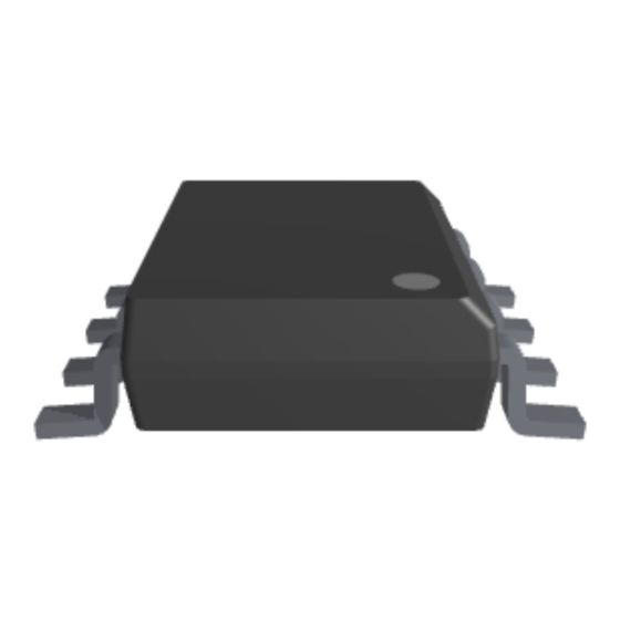
This EVM from TI is based on a 17-A, split output, basic insulation UCC5390SCD driver in a SOIC-8 package. The EVM also includes a SN6505B-based bias supply that can be configured for single or split-rail drive voltage from 11 V to 33 V, covering a wide range of Si and SiC FETs and IGBTs. -
Page 4: Ucc5390Scdevm-010 Board Image
UCC53xx family of drivers, in an 8-pin SOIC package including variants with different pinout configurations and drive strengths. For this design, the UCC5390SCD device, with split output, 17- A, and typical current capability, has been selected for its ability to optimally drive FETs and IGBTs in mid- and high-power applications. -
Page 5: Electrical Specifications
0.95 × 0.83 × 0.3 inch Detailed Description The following sections provide a detailed description of the EVM. SLLU282A – December 2017 – Revised February 2018 UCC5390SCD With Isolated Bias Supply Submit Documentation Feedback Copyright © 2017–2018, Texas Instruments Incorporated... -
Page 6: Ucc5390Scdevm-010 Electrical Schematic
By default, the EVM is configured for drive pulse outputs, 18 V to turn ON, and –4 V to turn OFF, when a 3.3-V supply voltage is applied to the input. Different settings are possible, described as follows. The configuration procedure is described based on the schematic shown in Figure Copyright © 2017, Texas Instruments Incorporated Figure 3. UCC5390SCDEVM-010 Electrical Schematic UCC5390SCD With Isolated Bias Supply SLLU282A –... - Page 7 Remove D1, D3, R7; place R5 and +7/–4 +13/-4 Bridge, split output Remove R7 and R6; place D1, D3, +18/-4 +30/–4 SLLU282A – December 2017 – Revised February 2018 UCC5390SCD With Isolated Bias Supply Submit Documentation Feedback Copyright © 2017–2018, Texas Instruments Incorporated...
-
Page 8: Test Summary
❏ All high voltage, high temperature, and hazard safety rules, applied to the power system where these EVMs are embedded for bench evaluation, must be strictly followed. UCC5390SCD With Isolated Bias Supply SLLU282A – December 2017 – Revised February 2018 Submit Documentation Feedback... - Page 9 Channel A Pulse 100 KHz 4.5 µs 0 ns 50 Ω Feed-thru 50 Ω Channel B 5 µs SLLU282A – December 2017 – Revised February 2018 UCC5390SCD With Isolated Bias Supply Submit Documentation Feedback Copyright © 2017–2018, Texas Instruments Incorporated...
-
Page 10: Soldering Ucc5390Scdevm-010 Board For System Level Evaluation
FET terminals. Figure 4. Soldering UCC5390SCDEVM-010 Board for System Level Evaluation UCC5390SCD With Isolated Bias Supply SLLU282A – December 2017 – Revised February 2018 Submit Documentation Feedback... -
Page 11: Power Up, Capturing Waveforms, And Power Down
6. Verify that gate voltages of the lower and upper FETs are similar to that shown in Figure SLLU282A – December 2017 – Revised February 2018 UCC5390SCD With Isolated Bias Supply Submit Documentation Feedback Copyright © 2017–2018, Texas Instruments Incorporated... -
Page 12: Gate-Source Driver Voltage
Figure 6. Gate-Source Driver Voltage 1. Expand the horizontal scale of oscilloscope from 2 µs/div to 10 ns/div, and verify rise and fall time of the driver board indicating high output current capability of UCC5390SCD driver ICs (Figure 7 Figure 2. -
Page 13: Expanded Gate-Source Drive Voltage Rise Time
12. Reduce the voltage of the low voltage supply down to 0 A. Power down is complete. Figure 7. Expanded Gate-Source Drive Voltage Rise Time SLLU282A – December 2017 – Revised February 2018 UCC5390SCD With Isolated Bias Supply Submit Documentation Feedback Copyright © 2017–2018, Texas Instruments Incorporated... -
Page 14: Expanded Gate-Source Drive Voltage Fall Time
Power Up, Capturing Waveforms, and Power Down www.ti.com Figure 8. Expanded Gate-Source Drive Voltage Fall Time UCC5390SCD With Isolated Bias Supply SLLU282A – December 2017 – Revised February 2018 Submit Documentation Feedback Copyright © 2017–2018, Texas Instruments Incorporated... -
Page 15: Inductor Current (Red), Drain-Source (Pink) And Gate-Source Drive Voltages (Blue And Green) At 800-V Input, 0-A Output
Figure 9. Inductor Current (Red), Drain-Source (Pink) and Gate-Source Drive Voltages (Blue and Green) at 800-V Input, 0-A Output SLLU282A – December 2017 – Revised February 2018 UCC5390SCD With Isolated Bias Supply Submit Documentation Feedback Copyright © 2017–2018, Texas Instruments Incorporated... -
Page 16: Expanded Soft Switching Waveforms During Vds Rise
Power Up, Capturing Waveforms, and Power Down www.ti.com Figure 10. Expanded Soft Switching Waveforms During Vds Rise UCC5390SCD With Isolated Bias Supply SLLU282A – December 2017 – Revised February 2018 Submit Documentation Feedback Copyright © 2017–2018, Texas Instruments Incorporated... -
Page 17: Expanded Soft Switching Waveforms During Vds Fall
Power Up, Capturing Waveforms, and Power Down www.ti.com Figure 11. Expanded Soft Switching Waveforms During Vds Fall SLLU282A – December 2017 – Revised February 2018 UCC5390SCD With Isolated Bias Supply Submit Documentation Feedback Copyright © 2017–2018, Texas Instruments Incorporated... -
Page 18: Inductor Current (Red), Drain-Source (Pink) And Gate-Source Drive Voltages (Blue And Green) At 800-V Input, 1.0-A Output
Figure 12. Inductor Current (Red), Drain-Source (Pink) and Gate-Source Drive Voltages (Blue and Green) at 800-V Input, 1.0-A Output UCC5390SCD With Isolated Bias Supply SLLU282A – December 2017 – Revised February 2018 Submit Documentation Feedback Copyright © 2017–2018, Texas Instruments Incorporated... -
Page 19: Expanded Hard, 71 V Per Ns Switching Waveforms During Vds Rise
Power Up, Capturing Waveforms, and Power Down www.ti.com Figure 13. Expanded Hard, 71 V per ns Switching Waveforms During Vds Rise SLLU282A – December 2017 – Revised February 2018 UCC5390SCD With Isolated Bias Supply Submit Documentation Feedback Copyright © 2017–2018, Texas Instruments Incorporated... -
Page 20: Expanded Soft, 3.4 V Per Ns Switching Waveforms During Vds Fall
Power Up, Capturing Waveforms, and Power Down www.ti.com Figure 14. Expanded Soft, 3.4 V per ns Switching Waveforms During Vds Fall UCC5390SCD With Isolated Bias Supply SLLU282A – December 2017 – Revised February 2018 Submit Documentation Feedback Copyright © 2017–2018, Texas Instruments Incorporated... -
Page 21: Bias Supply Performance
These measurements have been fulfilled only with the bias supply components populated onboard to avoid the impact of the driver circuit. Figure 15. Bias Supply Efficiency at Different Configurations SLLU282A – December 2017 – Revised February 2018 UCC5390SCD With Isolated Bias Supply Submit Documentation Feedback Copyright © 2017–2018, Texas Instruments Incorporated... - Page 22 Bias Supply Performance www.ti.com Figure 16. Bias Supply Regulation at Different Configurations UCC5390SCD With Isolated Bias Supply SLLU282A – December 2017 – Revised February 2018 Submit Documentation Feedback Copyright © 2017–2018, Texas Instruments Incorporated...
- Page 23 Bias Supply Performance www.ti.com Figure 17. Bias Supply Secondary Side Switching Waveforms SLLU282A – December 2017 – Revised February 2018 UCC5390SCD With Isolated Bias Supply Submit Documentation Feedback Copyright © 2017–2018, Texas Instruments Incorporated...
-
Page 24: Bill Of Materials
High CMTI, D0008B (SOIC-8) Texas SN6505BDBVR Texas Instruments Low-noise, 1 A, 420-KHz Transformer Driver, Instruments DBV0006A (SOT-6) UCC5390SCD With Isolated Bias Supply SLLU282A – December 2017 – Revised February 2018 Submit Documentation Feedback Copyright © 2017–2018, Texas Instruments Incorporated... -
Page 25: Layout Diagrams
Layout Diagrams www.ti.com Layout Diagrams Figure 18. Top Solder Mask Figure 19. Top Layer Figure 20. Bottom Layer SLLU282A – December 2017 – Revised February 2018 UCC5390SCD With Isolated Bias Supply Submit Documentation Feedback Copyright © 2017–2018, Texas Instruments Incorporated... - Page 26 Layout Diagrams www.ti.com Figure 21. Bottom Solder Mask Figure 22. Mechanical Dimensions UCC5390SCD With Isolated Bias Supply SLLU282A – December 2017 – Revised February 2018 Submit Documentation Feedback Copyright © 2017–2018, Texas Instruments Incorporated...
-
Page 27: References
Figure 23. Assembly Drawings References • Texas Instruments, UCC5390 Product Folder • Texas Instruments, SN6505B Product Folder SLLU282A – December 2017 – Revised February 2018 UCC5390SCD With Isolated Bias Supply Submit Documentation Feedback Copyright © 2017–2018, Texas Instruments Incorporated... - Page 28 ................per ns Switching Waveforms During Vds Fall image ............. • Added alternate part number and alternate manufacturer columns to BOM Revision History SLLU282A – December 2017 – Revised February 2018 Submit Documentation Feedback Copyright © 2017–2018, Texas Instruments Incorporated...
- Page 29 STANDARD TERMS FOR EVALUATION MODULES Delivery: TI delivers TI evaluation boards, kits, or modules, including any accompanying demonstration software, components, and/or documentation which may be provided together or separately (collectively, an “EVM” or “EVMs”) to the User (“User”) in accordance with the terms set forth herein.
- Page 30 FCC Interference Statement for Class B EVM devices NOTE: This equipment has been tested and found to comply with the limits for a Class B digital device, pursuant to part 15 of the FCC Rules. These limits are designed to provide reasonable protection against harmful interference in a residential installation.
- Page 31 【無線電波を送信する製品の開発キットをお使いになる際の注意事項】 開発キットの中には技術基準適合証明を受けて いないものがあります。 技術適合証明を受けていないもののご使用に際しては、電波法遵守のため、以下のいずれかの 措置を取っていただく必要がありますのでご注意ください。 1. 電波法施行規則第6条第1項第1号に基づく平成18年3月28日総務省告示第173号で定められた電波暗室等の試験設備でご使用 いただく。 2. 実験局の免許を取得後ご使用いただく。 3. 技術基準適合証明を取得後ご使用いただく。 なお、本製品は、上記の「ご使用にあたっての注意」を譲渡先、移転先に通知しない限り、譲渡、移転できないものとします。 上記を遵守頂けない場合は、電波法の罰則が適用される可能性があることをご留意ください。 日本テキサス・イ ンスツルメンツ株式会社 東京都新宿区西新宿6丁目24番1号 西新宿三井ビル 3.3.3 Notice for EVMs for Power Line Communication: Please see http://www.tij.co.jp/lsds/ti_ja/general/eStore/notice_02.page 電力線搬送波通信についての開発キットをお使いになる際の注意事項については、次のところをご覧ください。http:/ /www.tij.co.jp/lsds/ti_ja/general/eStore/notice_02.page 3.4 European Union 3.4.1 For EVMs subject to EU Directive 2014/30/EU (Electromagnetic Compatibility Directive): This is a class A product intended for use in environments other than domestic environments that are connected to a low-voltage power-supply network that supplies buildings used for domestic purposes.
- Page 32 Notwithstanding the foregoing, any judgment may be enforced in any United States or foreign court, and TI may seek injunctive relief in any United States or foreign court. Mailing Address: Texas Instruments, Post Office Box 655303, Dallas, Texas 75265 Copyright © 2018, Texas Instruments Incorporated...
- Page 33 IMPORTANT NOTICE FOR TI DESIGN INFORMATION AND RESOURCES Texas Instruments Incorporated (‘TI”) technical, application or other design advice, services or information, including, but not limited to, reference designs and materials relating to evaluation modules, (collectively, “TI Resources”) are intended to assist designers who are developing applications that incorporate TI products;...
- Page 34 Mouser Electronics Authorized Distributor Click to View Pricing, Inventory, Delivery & Lifecycle Information: Texas Instruments UCC5390SCDEVM-010...
Need help?
Do you have a question about the UCC5390SCD and is the answer not in the manual?
Questions and answers