Table of Contents
Advertisement
Quick Links
FEATURES SUMMARY
FAST 8-BIT 8032 MCU
–
40MHz at 5.0V, 24MHz at 3.3V
–
Core, 12-clocks per instruction
DUAL FLASH MEMORIES WITH MEMORY
MANAGEMENT
–
Place either memory into 8032 program
address space or data address space
–
READ-while-WRITE operation for In-
Application Programming and EEPROM
emulation
–
Single voltage program and erase
–
100K minimum erase cycles, 15-year
retention
CLOCK, RESET, AND SUPPLY
MANAGEMENT
–
SRAM is Battery Backup capable
www.BDTIC.com/ST
–
Normal, Idle, and Power Down Modes
–
Power-on and Low Voltage reset
supervisor
–
Programmable Watchdog Timer
PROGRAMMABLE LOGIC, GENERAL
PURPOSE
–
16 macrocells
–
Implements state machines, glue-logic,
and so forth
COMMUNICATION INTERFACES
2
–
I
C Master/Slave bus controller
–
Two UARTs with independent baud rate
–
Six I/O ports with up to 46 I/O pins
–
8032 Address/Data bus available on
TQFP80 package
–
5 PWM outputs, 8-bit resolution
–
USB v1.1, low-speed 1.5Mbps, 3
endpoints (uPSD3212A only)
December 2004
Flash Programmable System Devices with
8032 MCU with USB and Programmable Logic
uPSD3212A, uPSD3212C
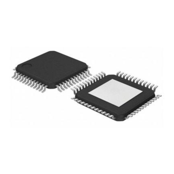
Figure 1. Packages
JTAG IN-SYSTEM PROGRAMMING
–
Program the entire device in as little as
10 seconds
A/D CONVERTER
–
Four channels, 8-bit resolution, 10µs
TIMERS AND INTERRUPTS
–
Three 8032 standard 16-bit timers
–
10 Interrupt sources with two external
interrupt pins
Single Supply Voltage
–
4.5 to 5.5V
–
3.0 to 3.6V
uPSD3212CV
TQFP52 (T)
52-lead, Thin,
Quad, Flat
TQFP80 (U)
80-lead, Thin,
Quad, Flat
1/163
Advertisement
Table of Contents

Related Manuals for ST UPSD3212A


Summary of Contents for ST UPSD3212A
-
Page 1: Features Summary
– 8032 Address/Data bus available on TQFP80 package – 5 PWM outputs, 8-bit resolution – USB v1.1, low-speed 1.5Mbps, 3 endpoints (uPSD3212A only) December 2004 uPSD3212A, uPSD3212C Flash Programmable System Devices with Figure 1. Packages JTAG IN-SYSTEM PROGRAMMING – Program the entire device in as little as... - Page 2 Table 1. Device Summary Part Number Clock Flash (MHz) (bytes) uPSD3212C-40T6 uPSD3212CV-24T6 uPSD3212C-40U6 uPSD3212CV-24U6 uPSD3212A-40T6 uPSD3212A-40U6 www.BDTIC.com/ST 2/163 SRAM Flash GPIO (bytes) (bytes) 8032 Pkg. 4.5-5.5 TQFP52 –40°C to 85°C 3.0-3.6 TQFP52 –40°C to 85°C 4.5-5.5 TQFP80 –40°C to 85°C 3.0-3.6 TQFP80 –40°C to 85°C...
-
Page 3: Table Of Contents
Power Control Register............39 uPSD3212A, uPSD3212C, uPSD3212CV... - Page 4 Idle Mode ..............39 Power-Down Mode .
- Page 5 PLD Power Management............124 uPSD3212A, uPSD3212C, uPSD3212CV...
- Page 6 PSD Chip Select Input (CSI, PD2) ..........124 Input Clock .
-
Page 7: Summary Description
P4.0:7 (8) GPIO, Port 4 USB+, USB v1.1 USB– uPSD3212A, uPSD3212C, uPSD3212CV Dual Flash memory banks provide a robust solu- tion for remote product updates in the field through In-Application Programming (IAP). Dual Flash banks also support EEPROM emulation, eliminat- ing the need for external EEPROM chips. - Page 8 Figure 3. TQFP52 Connections PD1/CLKIN JTAG TDO JTAG TDI USB– (1) PC4/TERR_ USB+ V CC PC3/TSTAT PC2/V STBY JTAG TCK JTAG TMS www.BDTIC.com/ST Note: 1. Pull-up resistor required on pin 5 (2k 8/163 for 3V devices, 7.5k for 5V devices).
- Page 9 NC (2) P4.7/PWM4 P4.6/PWM3 JTAG TMS Note: 1. Pull-up resistor required on pin 8 (2k 2. NC = Not Connected. uPSD3212A, uPSD3212C, uPSD3212CV for 3V devices, 7.5k for 5V devices). 60 P1.5/ADC1 59 P1.4/ADC0 58 P1.3/TXD1 57 A11 56 P1.2/RXD1 55 A10 54 P1.1/TX2...
- Page 10 Table 2. 80-Pin Package Pin Description Signal Port Pin Pin No. Name P1.0 P1.1 P1.2 RxD1 P1.3 TxD1 P1.4 ADC0 P1.5 ADC1 P1.6 ADC2 www.BDTIC.com/ST P1.7 ADC3 P3.0 RxD0 P3.1 TxD0 P3.2 EXINT0 P3.3 EXINT1 P3.4 P3.5 P3.6...
- Page 11 P4.6 PWM3 P4.7 PWM4 USB– PSEN_ RESET_ XTAL1 XTAL2 www.BDTIC.com/ST uPSD3212A, uPSD3212C, uPSD3212CV In/Out Basic General I/O port pin General I/O port pin General I/O port pin General I/O port pin Pull-up resistor required (2k devices, 7.5k for 5V devices)
-
Page 12: 52-Pin Package I/O Port
Signal Port Pin Pin No. Name JTAG TMS JTAG TCK STBY TSTAT TERR_ JTAG TDI JTAG TDO CLKIN www.BDTIC.com/ST USB+ 52-PIN PACKAGE I/O PORT The 52-pin package members of the uPSD321x Devices have the same port pins as those of the 80-pin package except: –... -
Page 13: Architecture Overview
64KB www.BDTIC.com/ST 16KB Flash Memory Space uPSD3212A, uPSD3212C, uPSD3212CV space. Refer to the PSD Module for details on mapping of the Flash memory. The 8032 core has two types of data memory (in- ternal and external) that can be read and written. -
Page 14: Registers
Registers The 8032 has several registers; these are the Pro- gram Counter (PC), Accumulator (A), B Register (B), the Stack Pointer (SP), the Program Status Word (PSW), General purpose registers (R0 to R7), and DPTR (Data Pointer register). -
Page 15: Program Memory
256 bytes of internal RAM, 128 bytes of Special Function Registers (SFRs) areas and 2K bytes (XRAM-PSD) in the PSD Mod- ule. uPSD3212A, uPSD3212C, uPSD3212CV AC FO RS1 RS0 OV Register Bank Select Flags (to select Bank0-3) Four register banks, each 8 registers wide, occupy locations 0 through 31 in the lower RAM area. -
Page 16: Sfr
The SFRs can only be addressed directly in the address range from 15., page 28 gives an overview of the Special Function Registers. Sixteen address in the SFRs space are both-byte and bit-addressable. The bit- addressable SFRs are those whose address ends in 0h and 8h. -
Page 17: Arithmetic Instructions
Accumulator data to the base pointer (see Figure 13). Example: movc A, @A+DPTR Figure 13. Indexed Addressing DPTR 1E73h uPSD3212A, uPSD3212C, uPSD3212CV register banks, Arithmetic Instructions The arithmetic instructions is listed in 4., page modes that can be used with each instruction to access the <byte>... -
Page 18: Logical Instructions
Table 4. Arithmetic Instructions Mnemonic ADD A,<byte> ADDC A,<byte> SUBB A,<byte> INC <byte> INC DPTR DEC <byte> MUL AB DIV AB DA A Logical Instructions Table 5., page 19 shows list of uPSD321x Devic- es logical instructions. The instructions that per-... - Page 19 Rotate A Left through Carry RR A RRC A Rotate A Right through Carry SWAP A www.BDTIC.com/ST uPSD3212A, uPSD3212C, uPSD3212CV Operation A = A .AND. <byte> A = <byte> .AND. A A = <byte> .AND. #data A = A .OR. <byte>...
-
Page 20: Data Transfers
Data Transfers Internal RAM. Table shows the menu of in- structions that are available for moving data around within the internal memory spaces, and the addressing modes that can be used with each one. The MOV <dest>, <src> instruction allows... - Page 21 ; loop for R1 = 2Dh ; loop for R1 = 2Ch ; loop for R1 = 2Bh A,2Ah uPSD3212A, uPSD3212C, uPSD3212CV Table 7. Shifting a BCD Number Two Digits to the Right (using direct MOVs: 14 bytes) A,2Eh 2Eh,2Dh...
- Page 22 External RAM. Table shows a list of the Data Transfer instructions that access external Data Memory. Only indirect addressing can be used. The choice is whether to use a one-byte address, @Ri, where Ri can be either R0 or R1 of the se-...
-
Page 23: Boolean Instructions
This code uses the JNB instruction, one of a series of bit-test instructions which execute a jump if the uPSD3212A, uPSD3212C, uPSD3212CV addressed bit is set (JC, JB, JBC) or if the ad- dressed bit is not set (JNC, JNB). In the above case, Bit 2 is being tested, and if bit2 = 0, the CPL C instruction is jumped over. -
Page 24: Jump Instructions
Jump Instructions Table shows the list of unconditional jump in- structions. The table lists a single “JMP add” in- struction, but in fact there are three SJMP, LJMP, and AJMP, which differ in the format of the desti- nation address. -
Page 25: Machine Cycles
DJNZ <byte>,rel Decrement and jump if not zero CJNE A,<byte>,rel CJNE <byte>,#data,rel uPSD3212A, uPSD3212C, uPSD3212CV Every time the loop was executed, R1 was decre- mented, and the looping was to continue until the R1 data reached 2Ah. Another application of this instruction is in “greater than, less than”... - Page 26 Figure 14. State Sequence in uPSD321x Devices Osc. (XTAL2) Read opcode a. 1-Byte, 1-Cycle Instruction, e.g. INC A Read opcode b. 2-Byte, 1-Cycle Instruction, e.g. ADD A, adrs Read opcode c. 1-Byte, 2-Cycle Instruction, e.g. INC DPTR www.BDTIC.com/ST...
-
Page 27: Upsd3200 Hardware Description
PSD MODULE Page Register Decode PLD JTAG ISP uPSD3212A, uPSD3212C, uPSD3212CV that have a port architecture which is different from Ports 0-4 in the MCU Module. The PSD Module communicates with the CPU Core through the internal address, data bus (A0- A15, D0-D7) and control signals (RD_, WR_, PSEN_ , ALE, RESET_). -
Page 28: Mcu Module Discription
MCU MODULE DISCRIPTION This section provides a detail description of the MCU Module system functions and Peripherals, including: Special Function Registers Timers/Counter Interrupts Supervisory Function (LVD and Watchdog) USART Power Saving Modes C Bus On-chip Oscillator I/O Ports Table 15. - Page 29 P4SFS P4S7 P4S6 ASCL ADAT ADAT7 ADAT6 ACON SCON SBUF SCON2 SBUF2 A1 PWMCON PWML PWMP PWM0 PWM1 uPSD3212A, uPSD3212C, uPSD3212CV Bit Register Name TCLK1 Gate P1S5 P1S4 P4S5 P4S4 P4S3 P4S2 ADAT5 ADAT4 ADAT3 ADAT2 ADEN ADS1 ADS0 PWME...
- Page 30 Reg Name Addr PWM2 PWM3 WDRST PWM4P PWM4W WDKEY PSCL0L www.BDTIC.com/ST PSCL0H PSCL1L PSCL1H T2CON EXF2 T2MOD RCAP2L RCAP2H 30/163 Bit Register Name RCLK TCLK EXEN2 Reset Value PI2C C/T2 CP/RL2 DCEN 00 Timer 2 Mode Comments...
- Page 31 — USTA RSEQ SETUP UADR USBEN UADD6 UADD5 UADD4 UDR0 UDR0.7 UDR0.6 UDR0.5 UDR0.4 UDR0.3 UDR0.2 UDR0.1 UDR0.0 uPSD3212A, uPSD3212C, uPSD3212CV Bit Register Name ADDR Intr TX-Md Bbusy Blost RSTF TXD0F RXD0F RXD1F RSTFIE TXD0IE RXD0IE TXD1IE EOPIE RESUMIE 00...
- Page 32 Table 17. PSD Module Register Address Offset CSIOP Addr Register Name Offset Data In (Port A) Configure pin between I/O or Address Out Mode. Bit = 0 selects I/ Control (Port A) Data Out (Port A) Direction (Port A) Configures Port pin as input or output.
- Page 33 Note: (Register address = csiop address + address offset; where csiop address is defined by user in PSDsoft) * indicates bit is not used and need to set to '0.' uPSD3212A, uPSD3212C, uPSD3212CV Bit Register Name Sec3_ Sec2_...
-
Page 34: Interrupt System
INTERRUPT SYSTEM There are interrupt requests from 10 sources as follows (see Figure 16., page 35). INT0 External Interrupt 2nd USART Interrupt Timer 0 Interrupt C Interrupt INT1 External Interrupt (or ADC Interrupt) Timer 1 Interrupt USB Interrupt... - Page 35 Figure 16. Interrupt System Interrupt Sources INT0 USART Timer INT1 Timer USART Timer www.BDTIC.com/ST uPSD3212A, uPSD3212C, uPSD3212CV IP / IPA Priority IE / Global Enable High AI07427b 35/163...
-
Page 36: Usart Interrupt
USART Interrupt – The USART Interrupt is generated by RI (Receive Interrupt) OR TI (Transmit Interrupt). – When the USART Interrupt is generated, the corresponding request flag must be cleared by the software. The interrupt service routine will... - Page 37 — Reserved — Reserved Timer 2 Interrupt priority level USART Interrupt priority level Timer 1 Interrupt priority level External Interrupt (Int1) priority level Timer 0 Interrupt priority level External Interrupt (Int0) priority level uPSD3212A, uPSD3212C, uPSD3212CV Function Function Function 37/163...
-
Page 38: How Interrupts Are Handled
Table 23. Description of the IPA Bits Symbol — Not used — Not used — Not used 2nd USART Interrupt priority level — Not used — Not used PI2C I²C Interrupt priority level PUSB USB Interrupt priority level... -
Page 39: Power-Saving Mode
Table 26. Pin Status During Idle and Power-down Mode Addr Name PCON SMOD SMOD1 LVREN ADSFINT RCLK1 uPSD3212A, uPSD3212C, uPSD3212CV Power Control Register The Idle and Power-down Modes are activated by software via the PCON register (see Tables Table 27., page Idle Mode The instruction that sets PCON.0 is the last in-... -
Page 40: I/O Ports (Mcu Module)
Table 27. Description of the PCON Bits Symbol SMOD Double Baud Data Rate Bit UART SMOD1 Double Baud Data Rate Bit 2nd UART LVREN LVR Disable Bit (active High) ADSFINT Enable ADC Interrupt Received Clock Flag (UART 2) - Page 41 0=Port 4.7 0=Port 4.6 0=Port 4.5 1=PWM 4 1=PWM 3 1=PWM 2 uPSD3212A, uPSD3212C, uPSD3212CV or I C bus pins. The READ and WRITE pins are assigned to dedicated pins. Port 3 (I trolled using the P3SFS and P4SFS Special Func- tion Selection registers.
-
Page 42: Port Type And Description
PORT Type and Description Figure 17. PORT Type and Description (Part 1) In / Symbol RESET WR, RD,ALE, PSEN XTAL1, XTAL2 www.BDTIC.com/ST PORT0 42/163 Circuit • Schmitt input with internal pull-up CMOS compatible interface NFC : 400ns... - Page 43 Symbol PORT1 <3:0>, PORT3, PORT4<7:3,1:0> PORT2 PORT1 < 7:4 > PORT4.2 www.BDTIC.com/ST USB–, USB+ uPSD3212A, uPSD3212C, uPSD3212CV Circuit Bidirectional I/O port with Schmitt input CMOS compatible interface Bidirectional I/O port with Schmitt input CMOS compatible interface Analog input option an_enb Bidirectional I/O port with internal Schmitt input.
-
Page 44: Oscillator
OSCILLATOR The oscillator circuit of the uPSD321x Devices is a single stage inverting amplifier in a Pierce oscilla- tor configuration (see Figure 19). The circuitry be- tween XTAL1 and XTAL2 is basically an inverter biased to the transfer point. Either a crystal or ce- ramic resonator can be used as the feedback ele- Figure 19. -
Page 45: Supervisory
Figure 20. RESET Configuration www.BDTIC.com/ST Reset RSTE USB Reset uPSD3212A, uPSD3212C, uPSD3212CV before it is released. On initial power-up the LVR is enabled (default). After power-up the LVR can be disabled via the LVREN Bit in the PCON Reg- ister. -
Page 46: Watchdog Timer
WATCHDOG TIMER The hardware Watchdog Timer (WDT) resets the uPSD321x Devices when it overflows. The WDT is intended as a recovery method in situations where the CPU may be subjected to a software upset. To prevent a system reset the timer must be reloaded in time by the application software. - Page 47 WDRST0 For example: MOV WDRST,#1EH Note: The Watchdog Timer (WDT) is enabled at power-up or reset and must be served or disabled. uPSD3212A, uPSD3212C, uPSD3212CV x 12 x 2 x 12 x 2 Reset pulse width (about 10ms at 40Mhz, about 50ms at 8Mhz) Reset period (1.258 second at 40Mhz)
-
Page 48: Timer/Counters (Timer 0, Timer 1 And Timer 2)
TIMER/COUNTERS (TIMER 0, TIMER 1 AND TIMER 2) The uPSD321x Devices has three 16-bit Timer/ Counter registers: Timer 0, Timer 1 and Timer 2. All of them can be configured to operate either as timers or event counters and are compatible with standard 8032 architecture. - Page 49 (M1,M0)=(1,0): 8-bit auto-reload Timer/Counter. TH0 holds a value which is to be reloaded into TL0 each time it overflows (M1,M0)=(1,1): TL0 is an 8-bit Timer/Counter controlled by the standard TImer 0 control bits. TH0 is an 8-bit timer only controlled by Timer 1 control bits www.BDTIC.com/ST uPSD3212A, uPSD3212C, uPSD3212CV Function 49/163...
- Page 50 Mode 0. Putting either Timer into Mode 0 makes it look like an 8048 Timer, which is an 8-bit Counter with a divide-by-32 prescaler. Figure Mode 0 operation as it applies to Timer 1. In this mode, the Timer register is configured as a 13-bit register.
-
Page 51: Timer 2
Gate INT1 pin Table 40. Timer/Counter 2 Control Register (T2CON) EXF2 uPSD3212A, uPSD3212C, uPSD3212CV 1-to-0 transition at external input T2EX causes the current value in the Timer 2 registers, TL2 and TH2, to be captured into registers RCAP2L and RCAP2H, respectively. In addition, the transition at T2EX causes Bit EXF2 in T2CON to be set, and EXF2 like TF2 can generate an interrupt. - Page 52 Table 41. Timer/Counter 2 Operating Modes T2CON RxCLK Mode TxCLK 16-bit Auto- reload 16-bit Capture Baud Rate Generator Note: = falling edge Table 42. Description of the T2CON Bits Symbol www.BDTIC.com/ST Timer 2 Overflow Flag. Set by a Timer 2 overflow, and must be cleared by software. TF2...
- Page 53 Figure 25. Timer 2 in Auto-Reload Mode www.BDTIC.com/ST ÷ 12 C/T2 = 0 C/T2 = 1 T2 pin Transition Detector T2EX pin EXEN2 uPSD3212A, uPSD3212C, uPSD3212CV (8 bits) (8 bits) Control Capture RCAP2L RCAP2H Control (8 bits) (8 bits) Control...
- Page 54 Mode 3. Timer 1 in Mode 3 simply holds its count. The effect is the same as setting TR1 = 0. Timer 0 in Mode 3 establishes TL0 and TH0 as two separate counters. The logic for Mode 3 on Timer 0 is shown in Figure 26.
-
Page 55: Standard Serial Interface (Uart)
Stop Bit is ignored. The baud rate is pro- grammable to either 1/32 or 1/64 the oscillator fre- quency. uPSD3212A, uPSD3212C, uPSD3212CV Mode 3. 11 bits are transmitted (through TxD) or received (through RxD): a Start Bit (0), 8 data bits (LSB first), a programmable 9th data bit, and a Stop Bit (1). -
Page 56: Serial Port Control Register
Serial Port Control Register The serial port control and status register is the Special Function Register SCON (SCON2 for the second port), shown in Figure 27. This register (see Tables and 44) contains not only the mode Figure 27. - Page 57 Receive Interrupt Flag. Set by hardware at the end of the 8th bit time in Mode 0, or halfway through the Stop Bit in the other modes, in any serial reception (except for SM2). Must be cleared by software www.BDTIC.com/ST uPSD3212A, uPSD3212C, uPSD3212CV Function /64 or f 57/163...
- Page 58 Baud Rates. The baud rate in Mode 0 is fixed: Mode 0 Baud Rate = f / 12 The baud rate in Mode 2 depends on the value of Bit SMOD = 0 (which is the value on reset), the baud rate is 1/64 the oscillator frequency.
- Page 59 When the MSB of the data byte is at the output position of the shift register, then the '1' that was initially loaded into the 9th position, is just uPSD3212A, uPSD3212C, uPSD3212CV SMOD to the left of the MSB, and all positions to the left of that contain zeros.
- Page 60 Figure 28. Serial Port Mode 0, Waveforms Write to SBUF S6P2 Send Shift RxD (Data Out) TxD (Shift Clock) Write to SCON Clear RI Receive Shift RxD (Data In) TxD (Shift Clock) More About Mode 1. Ten bits are transmitted (through TxD), or received (through RxD): a start Bit (0), 8 data bits (LSB first).
- Page 61 Tx Clock Write to SBUF S1P1 Send Data Shift Start Bit ÷16 Reset Rx Clock Start Bit Bit Detector Sample Times Shift uPSD3212A, uPSD3212C, uPSD3212CV Zero Detector Start Tx Control ÷16 Tx Clock Serial Port Interrupt ÷16 Sample Rx Clock 1-to-0...
- Page 62 More About Modes 2 and 3. Eleven transmitted (through TxD), or received (through RxD): a Start Bit (0), 8 data bits (LSB first), a pro- grammable 9th data bit, and a Stop Bit (1). On transmit, the 9th data bit (TB8) can be assigned the value of '0' or '1.' On receive, the data bit goes...
- Page 63 S1P1 Send Data Shift Start Bit Stop Bit Generator ÷16 Reset Rx Clock Start Bit Bit Detector Sample Times Shift uPSD3212A, uPSD3212C, uPSD3212CV Zero Detector Start Tx Control ÷16 Tx Clock Serial Port Interrupt ÷16 Sample Rx Clock 1-to-0 Rx Control...
- Page 64 Figure 33. Serial Port Mode 3, Block Diagram Timer1 Timer2 Overflow Overflow Write SBUF ÷2 SMOD TCLK RCLK www.BDTIC.com/ST Figure 34. Serial Port Mode 3, Waveforms Tx Clock Write to SBUF S1P1 Send Data Shift Start Bit...
-
Page 65: Analog-To-Digital Convertor (Adc)
ACH1 ACH2 ACH3 ACON uPSD3212A, uPSD3212C, uPSD3212CV matically when A/D conversion is completed, cleared when A/D conversion is in process. The ASCL should be loaded with a value that re- sults in a clock rate of approximately 6MHz for the ADC using the following formula (see 48., page... - Page 66 Table 46. ADC SFR Memory Map Addr Name ASCL ADAT ADAT7 ADAT6 ACON Table 47. Description of the ACON Bits Symbol 7 to 6 — Reserved ADEN ADC Enable Bit: 0 : ADC shut off and consumes no operating current —...
-
Page 67: Pulse Width Modulation (Pwm)
PWM output is set LOW (with PWML = 0). The pulse-width-ratio is therefore de- www.BDTIC.com/ST uPSD3212A, uPSD3212C, uPSD3212CV fined by the contents of the corresponding Special Function Register (PWM 0-3) of a PWM. By load- ing the corresponding Special Function Register... - Page 68 Figure 36. Four-Channel 8-bit PWM Block Diagram 16-bit Prescaler CPU rd/wr (B2h,B1h) www.BDTIC.com/ST 16-bit Prescaler load PWMCON bit5 (PWME) 68/163 DATA BUS 8-bit PWM0-PWM3 CPU rd/wr Data Registers 8-bit PWM0-PWM3 Comparators Registers 8-bit PWM0-PWM3 Register Comparators 8-bit Counter...
- Page 69 PWML = PWM 0-3 polarity control – PWMP = PWM 4 polarity control – PWME = PWM enable (0 = disabled, 1= enabled) uPSD3212A, uPSD3212C, uPSD3212CV Bit Register Name PWME CFG4 CFG3 – CFG3..CFG0 = PWM 0-3 Output (0 = Open Drain;...
-
Page 70: Programmable Period 8-Bit Pwm
Programmable Period 8-bit PWM The PWM 4 channel can be programmed to pro- vide a PWM output with variable pulse width and period. The PWM 4 has a 16-bit Prescaler, an 8- bit Counter, a Pulse Width Register, and a Period Register. -
Page 71: Pwm 4 Channel Operation
Figure 38. PWM 4 With Programmable Pulse Width and Frequency www.BDTIC.com/ST PWM4 Defined by Pulse uPSD3212A, uPSD3212C, uPSD3212CV Counter output. When the content of the counter is equal to or greater than the value in the Pulse Width Register, it sets the PWM 4 output to low (with PWMP Bit = 0). -
Page 72: I 2 C Interface
C INTERFACE The serial port supports the twin line I sisting of a data line (SDA1), and a clock line (SCL1) as shown in Figure 39. Depending on the configuration, the SDA1 and SCL1 lines may re- quire pull-up resistors. - Page 73 These two bits along with the CR2 Bit determine the serial clock frequency when SIO is in the Master Mode. www.BDTIC.com/ST Table 52. Selection of the Serial Clock Frequency SCL in Master Mode uPSD3212A, uPSD3212C, uPSD3212CV Divisor 12MHz 12.5 6.25...
-
Page 74: Serial Status Register (S2Sta)
Serial Status Register (S2STA) S2STA is a “Read-only” register. The contents of this register may be used as a vector to a service routine. This optimized the response time of the software and consequently that of the I status codes for all possible modes of the I interface are given Table 54. -
Page 75: Address Register (S2Adr)
/2 – > 66.6ns) 20MHz (f /2 – > 100ns) 8MHz (f /2 – > 250ns) uPSD3212A, uPSD3212C, uPSD3212CV the I to work with the large range of MCU frequency val- ues supported. For example, with a system clock of 40MHz. -
Page 76: Usb Hardware
USB HARDWARE The characteristics of USB hardware are as fol- lows: Complies with the Universal Serial Bus specification Rev. 1.1 Integrated SIE (Serial Interface Engine), FIFO memory and transceiver Low speed (1.5Mbit/s) device capability Supports control endpoint0 and interrupt... - Page 77 RSTFIE TXD0IE RXD0IE TXD1IE EOPIE RESUMI www.BDTIC.com/ST uPSD3212A, uPSD3212C, uPSD3212CV TXD0IE RXD0IE Enable SUSPND Interrupt Enable USB Reset; also resets the CPU and PSD Modules when bit is set to '1.' Enable RSTF (USB Bus Reset Flag) Interrupt Enable TXD0 Interrupt...
- Page 78 Table 64. USB Interrupt Status Register (UISTA: 0E8h) SUSPND — Table 65. Description of the UISTA Bits Symbol SUSPND — RSTF TXD0F www.BDTIC.com/ST RXD0F TXD1F EOPF RESUMF 78/163 RSTF TXD0F RXD0F USB Suspend Mode Flag. To save power, this bit should be set if a 3ms constant idle state is detected on USB bus.
- Page 79 TX0E RX0E www.BDTIC.com/ST TP0SIZ3 to 3 to 0 TP0SIZ0 uPSD3212A, uPSD3212C, uPSD3212CV TX0E RX0E TP0SIZ3 Endpoint0 Data Sequence Bit. (0=DATA0, 1=DATA1) This bit determines which type of data packet (DATA0 or DATA1) will be sent during the next IN transaction. Toggling of this bit must be controlled by software.
- Page 80 Table 68. USB Endpoint1 (and 2) Transmit Control Register (UCON1: 0EBh) TSEQ1 EP12SEL Table 69. Description of the UCON1 Bits Symbol TSEQ1 EP12SEL TX1E www.BDTIC.com/ST FRESUM TP1SIZ3 to 3 to 0 TP1SIZ0 80/163 TX1E FRESUM TP1SIZ3 Endpoint 1/ Endpoint 2 Transmit Data Packet PID. (0=DATA0, 1=DATA1) This bit determines which type of data packet (DATA0 or DATA1) will be sent during the next IN transaction directed to Endpoint 1 or Endpoint 2.
- Page 81 Table 75. USB Endpoint0 Data Transmit Register (UDT0: 0E7h) UDT0.7 UDT0.6 UDT0.5 Table 76. USB Endpoint1 Data Transmit Register (UDT1: 0E6h) UDT1.7 UDT1.6 UDT1.5 uPSD3212A, uPSD3212C, uPSD3212CV — SOUT EP2E — Reserved Status out is used to automatically respond to the OUT of a control READ transfer Endpoint2 enable.
- Page 82 The USCL 8-bit Prescaler Register for USB is at E1h. The USCL should be loaded with a value that results in a clock rate of 6MHz for the USB using the following formula: USB clock input =...
-
Page 83: Transceiver
(max) www.BDTIC.com/ST Driver Signal Pins (min) uPSD3212A, uPSD3212C, uPSD3212CV fol- tolerates a voltage on the signal pins of -0.5V to 3.6V with respect to local ground reference without damage. The driver tolerates this voltage for 10.0µs while the driver is active and driving, and tolerates this condition indefinitely when the driver is in its high impedance state. - Page 84 Table 78. Transceiver DC Characteristics Symb Parameter Static Output High Static Output Low Differential Input Sensitivity Differential Input Common Mode Single Ended Receiver Threshold Transceiver Capacitance Data Line (D+, D-) Leakage External Bus Pull-up Resistance, D- External Bus Pull-down Resistance Note: 1.
-
Page 85: Receiver Characteristics
Figure 41. Figure 41. Differential Input Sensitivity Over Entire Common Mode Range www.BDTIC.com/ST uPSD3212A, uPSD3212C, uPSD3212CV tolerates static input voltages between -0.5V to 3.8V with respect to its local ground reference without damage. In addition to the differential re- ceiver, there is a single-ended receiver for each of the two data lines. -
Page 86: External Usb Pull-Up Resistor
External USB Pull-Up Resistor The USB system specifies a pull-up resistor on the D- pin for low-speed peripherals. The USB Spec 1.1 describes a 1.5k pull-up resistor to a 3.3V supply. An approved alternative method is a 7.5k pull-up to the USB V... - Page 87 Figure 44. Differential to EOP Transition Skew and EOP Width PERIOD Differential Data Lines Figure 45. Differential Data Jitter PERIOD Differential www.BDTIC.com/ST Data Lines uPSD3212A, uPSD3212C, uPSD3212CV Crossover Crossover Point Extended Point Diff. Data to SE0 Skew PERIOD DEOP Crossover...
-
Page 88: Psd Module
PSD MODULE The PSD Module provides configurable Program and Data memories to the 8032 CPU core (MCU). In addition, it has its own set of I/ O ports and a PLD with 16 macrocells for general logic implementation. - Page 89 Figure 46. PSD MODULE Block Diagram www.BDTIC.com/ST AI07431 89/163...
-
Page 90: In-System Programming (Isp)
In-System Programming (ISP) Using the JTAG signals on Port C, the entire PSD MODULE device can be programmed or erased without the use of the MCU. The primary Flash memory can also be programmed in-system by the MCU executing the programming algorithms out of the secondary memory, or SRAM. -
Page 91: Development System
Merge MCU Firmware with PSD Module Configuration A composite object file is created containing MCU firmware and uPSD3212A, uPSD3212C, uPSD3212CV dress is given on the back page of this data sheet) or other distribution channels. PSDsoft directly supports a low cost device pro- grammer from ST: FlashLINK (JTAG). -
Page 92: Psd Module Register Description And Address Offset
PSD MODULE REGISTER DESCRIPTION AND ADDRESS OFFSET Table shows the offset addresses to the PSD MODULE registers relative to the CSIOP base ad- dress. The CSIOP space is the 256 bytes of ad- dress that is allocated by the user to the internal Table 81. -
Page 93: Psd Module Detailed Operation
During a Program or Erase cycle in Flash memory, the status can be output on Ready/Busy (PC3). This pin is set up using PSDsoft Express Configu- ration. uPSD3212A, uPSD3212C, uPSD3212CV 27, the PSD MOD- Memory Block Select Signals The DPLD generates the Select signals for all the... -
Page 94: Instructions
Instructions An instruction consists of a sequence of specific operations. Each received byte is sequentially de- coded by the PSD MODULE and not executed as a standard WRITE operation. The instruction is ex- ecuted when the correct number of bytes are prop-... - Page 95 18. The MCU cannot invoke these instructions while executing code from the same Flash memory as that for which the instruction is intended. The MCU must retrieve, for example, the code from the secondary Flash memory when reading the Sector Protection Status of the primary Flash memory. uPSD3212A, uPSD3212C, uPSD3212CV Cycle 1 Cycle 2 Cycle 3 “Read”...
-
Page 96: Power-Down Instruction And Power-Up Mode
Power-down Instruction and Power-up Mode Power-up Mode. The PSD MODULE internal logic is reset upon Power-up to the READ Mode. Sector Select (FS0-FS3 CSBOOT1) must be held Low, and WRITE Strobe (WR, CNTL0) High, during Power-up for maximum... - Page 97 Note: 1. X = Not guaranteed value, can be read either '1' or '0.' 2. DQ7-DQ0 represent the Data Bus bits, D7-D0. 3. FS0-FS3 and CSBOOT0-CSBOOT1 are active High. uPSD3212A, uPSD3212C, uPSD3212CV bit is set to '1' when there is a failure during Flash memory Byte Program, Sector Erase, or Bulk Erase cycle.
-
Page 98: Programming Flash Memory
Programming Flash Memory Flash memory must be erased prior to being pro- grammed. A byte of Flash memory is erased to all '1s' (FFh), and is programmed by setting selected bits to '0.' The MCU may erase Flash memory all at once or by-sector, but not byte-by-byte. - Page 99 A '1' on the Error Flag Bit (DQ5) indi- cates a time-out condition on the Erase cycle; a '0' uPSD3212A, uPSD3212C, uPSD3212CV indicates no error. The MCU can read any location within the sector being erased to get the Toggle Flag Bit (DQ6) and the Error Flag Bit (DQ5).
-
Page 100: Erasing Flash Memory
Erasing Flash Memory Flash Bulk Erase. The Flash Bulk Erase instruc- tion uses six WRITE operations followed by a READ operation of the status register, as de- scribed in Table 82. If any byte of the Bulk Erase... -
Page 101: Specific Features
Sec<i>_Prot 0 = Secondary Flash memory Sector <i> is not write-protected. Security_Bit 0 = Security Bit in device has not been set; 1 = Security Bit in device has been set. uPSD3212A, uPSD3212C, uPSD3212CV primary Reset Flash. The Reset Flash instruction con- sists 82., page... -
Page 102: Sram
SRAM The SRAM is enabled when SRAM Select (RS0) from the DPLD is High. SRAM Select (RS0) can contain up to two product terms, allowing flexible memory mapping. The SRAM can be backed up using an external battery. - Page 103 PIO Mode www.BDTIC.com/ST uPSD3212A, uPSD3212C, uPSD3212CV For example, you may wish to have SRAM and pri- mary Flash memory in the Data space at Boot-up, and secondary Flash memory in the Program space at Boot-up, and later swap the primary and secondary Flash memories.
- Page 104 Separate Space Mode. Program space is sepa- rated from Data space. For example, Program Se- lect Enable (PSEN) is used to access the program code from the primary Flash memory, while READ Strobe (RD) is used to access data from the sec- ondary Flash memory, SRAM and I/O Port blocks.
-
Page 105: Page Register
(RS0) equations. Figure 53. Page Register www.BDTIC.com/ST uPSD3212A, uPSD3212C, uPSD3212CV If memory paging is not needed, or if not all 8 page register bits are needed for memory paging, then these bits may be used in the CPLD for general logic. -
Page 106: Plds
PLDS The PLDs bring programmable logic functionality to the uPSD. After specifying the logic for the PLDs in PSDsoft Express, the logic is pro- grammed into the device and available upon Pow- er-up. Table 87. DPLD and CPLD Inputs... - Page 107 CPLD www.BDTIC.com/ST DIRECT MACROCELL INPUT TO MCU DATA BUS INPUT MACROCELL & INPUT PORTS Note: 1. Ports A is not available in the 52-pin package uPSD3212A, uPSD3212C, uPSD3212CV PRIMARY FLASH MEMORY SELECTS SECONDARY NON-VOLATILE MEMORY SELECTS SRAM SELECT CSIOP SELECT...
-
Page 108: Decode Pld (Dpld)
Decode PLD (DPLD) The DPLD, shown in Figure 55, is used for decod- ing the address for PSD MODULE and external components. The DPLD can be used to generate the following decode signals: – 4 Sector Select (FS0-FS3) signals for the... -
Page 109: Complex Pld (Cpld)
PT OUTPUT ENABLE ( OE ) MACROCELL FEEDBACK I/O PORT INPUT PT INPUT LATCH GATE/CLOCK uPSD3212A, uPSD3212C, uPSD3212CV AND Array capable of generating up to 137 product terms Four I/O Ports. Each of the blocks are described in the sections that follow. -
Page 110: Output Macrocell (Omc)
Output Macrocell (OMC) Eight of the Output Macrocells (OMC) are con- nected to Ports A and B pins and are named as McellAB0-McellAB7. The other eight macrocells are connected to Ports B and C pins and are named as McellBC0-McellBC7. -
Page 111: Product Term Allocator
MACROCELL CS ALLOCATOR PT CLK CLKIN uPSD3212A, uPSD3212C, uPSD3212CV This is called product term expansion. PSDsoft Express performs this expansion as needed. Loading and Reading the Output Macrocells (OMC). The Output Macrocells (OMC) block oc- cupies a memory location in the MCU address... -
Page 112: Input Macrocells (Imc)
The OMC Mask Register. There is one Mask Register for each of the two groups of eight Output Macrocells (OMC). The Mask Registers can be used to block the loading of data to individual Out- put Macrocells (OMC). The default value for the Mask Registers is 00h, which allows loading of the Output Macrocells (OMC). -
Page 113: I/O Ports (Psd Module)
CONTROL REG. DIR REG. ENABLE PRODUCT TERM ( .OE ) CPLD-INPUT uPSD3212A, uPSD3212C, uPSD3212CV port pin has been defined, that pin is no longer available for other purposes. Exceptions are not- As shown in Figure 59, the ports contain an output... -
Page 114: Port Operating Modes
The Port pin’s tri-state output driver enable is con- trolled by a two input OR gate whose inputs come from the CPLD AND Array enable product term and the Direction Register. If the enable product term of any of the Array outputs are not defined... - Page 115 Note: 1. The direction of the Port A,B,C, and D pins are controlled by the Direction Register ORed with the individual output enable product term (.oe) from the CPLD AND Array. Table 91. I/O Port Latched Address Output Assignments Port A (PA3-PA0) Address a3-a0 Address a7-a4 uPSD3212A, uPSD3212C, uPSD3212CV PSEL D0 - D7 DATA BUS Port B Port A Yes (A7 –...
-
Page 116: Port Configuration Registers (Pcr)
Port Configuration Registers (PCR) Each Port has a set of Port Configuration Regis- ters (PCR) used for configuration. The contents of the registers can be accessed by the MCU through normal READ/WRITE bus cycles at the addresses given in Table 81., page... -
Page 117: Port Data Registers
Data Out Output Macrocell Mask Macrocell Input Macrocell Enable Out uPSD3212A, uPSD3212C, uPSD3212CV Register Bits are not set, writing to the macrocell loads data to the macrocell flip-flops. See PLDs, page OMC Mask Register. Each OMC Mask Register Bit corresponds to an Output Macrocell (OMC) flip- flop. -
Page 118: Ports A And B - Functionality And Structure
Ports A and B – Functionality and Structure Ports A and B have similar functionality and struc- ture, as shown in Figure 61. The two ports can be configured to perform one or more of the following... -
Page 119: Port C - Functionality And Structure
ENABLE PRODUCT TERM ( .OE ) CPLD - INPUT Note: 1. ISP or battery back-up uPSD3212A, uPSD3212C, uPSD3212CV Open Drain – Port C pins can be configured in Open Drain Mode Battery Backup features – PC2 can be configured for a battery input supply, Voltage... -
Page 120: Port D - Functionality And Structure
Port D – Functionality and Structure Port D has two I/O pins (only one pin, PD1, in the 52-pin package). See Figure 64., page 121. This port does not support Address Out Mode, and therefore no Control Register is re- quired. -
Page 121: External Chip Select
Chip Select (ECS1-ECS2) consists of one product Figure 64. Port D External Chip Select Signals www.BDTIC.com/ST uPSD3212A, uPSD3212C, uPSD3212CV term that can be configured active High or Low. The output enable of the pin is controlled by either the output enable product term or the Direction Register. -
Page 122: Power Management
POWER MANAGEMENT All PSD MODULE offers configurable power sav- ing options. These options may be used individu- ally or in combinations, as follows: – The primary and secondary Flash memory, and SRAM blocks are built with power management technology. - Page 123 Mode because you don’t want to have to wait for the logic and I/O to “wake-up” before their outputs can change. See Table down Mode effects on PSD MODULE ports. uPSD3212A, uPSD3212C, uPSD3212CV – Typical standby current is of the order of microamperes. These standby current values assume that there are no transitions on any PLD input.
-
Page 124: Pld Power Management
PLD Power Management The power and speed of the PLDs are controlled by the Turbo Bit (Bit 3) in PMMR0 (see Table 99). By setting the bit to '1,' the Turbo Mode is off and the PLDs consume the specified standby current when the inputs are not switching for an extended time of 70ns. - Page 125 Note: The bits of this register are cleared to zero following Power-up. Subsequent RESET pulses do not clear the registers. Table 101. APD Counter Operation APD Enable Bit www.BDTIC.com/ST uPSD3212A, uPSD3212C, uPSD3212CV Not used, and should be set to zero. Not used, and should be set to zero. Not used, and should be set to zero.
-
Page 126: Reset Timing And Device Status At Reset
RESET TIMING AND DEVICE STATUS AT RESET Upon Power-up, the PSD MODULE requires a Re- set (RESET) pulse of duration t is steady. During this period, the device loads in- ternal configurations, clears some of the registers and sets the Flash memory into operating mode. -
Page 127: Programming In-Circuit Using The Jtag Serial Interface
Table 103. JTAG Port Signals Port C Pin JTAG Signals TSTAT TERR uPSD3212A, uPSD3212C, uPSD3212CV JTAG Extensions TSTAT and TERR are two JTAG extension signals enabled by an “ISC_ENABLE” command received over the four standard JTAG signals (TMS, TCK, TDI, and TDO). They are used to speed Program... -
Page 128: Ac/Dc Parameters
AC/DC PARAMETERS These tables describe the AD and DC parameters of the uPSD321x Devices: DC Electrical Specification AC Timing Specification PLD Timing – Combinatorial Timing – Synchronous Clock Mode – Asynchronous Clock Mode – Input Macrocell Timing MCU Module Timing –... - Page 129 = 20mA x 40% + 28.45mA x 40% + 250µA x 60% This is the operating power with no Flash memory Erase or Program cycles in progress. Calculation is based on all I/O pins being disconnected and I uPSD3212A, uPSD3212C, uPSD3212CV Conditions = 12MHz...
-
Page 130: Maximum Rating
MAXIMUM RATING Stressing the device above the rating listed in the Absolute Maximum Ratings” table may cause per- manent damage to the device. These are stress ratings only and operation of the device at these or any other conditions above those indicated in the Operating sections of this specification is not im- Table 105. -
Page 131: Emc Characteristics
Parameter Electro-static discharge voltage (Human ESD(HBM) Body Model) Note: 1. Data based on characterization results, not tested in production uPSD3212A, uPSD3212C, uPSD3212CV Software Recommendations. The flowchart must include the management of ‘run- away’ conditions, such as: – Corrupted program counter –... - Page 132 LU. 3 complementary static tests are required on 10 parts to assess the latch-up performance. A supply overvoltage (applied to each power supply pin) and a current injection (applied to each input, output, and configurable I/O pin) are performed on each sample.
-
Page 133: Dc And Ac Parameters
Output Data RD signal WR signal Output STBY Output Macrocell uPSD3212A, uPSD3212C, uPSD3212CV ment Conditions summarized in the relevant tables. Designers should check that the operating conditions in their circuit match the measurement conditions when relying on the quoted parame- ters. - Page 134 Figure 70. Switching Waveforms – Key WAVEFORMS www.BDTIC.com/ST 134/163 INPUTS OUTPUTS STEADY INPUT STEADY OUTPUT MAY CHANGE FROM WILL BE CHANGING HI TO LO FROM HI TO LO MAY CHANGE FROM WILL BE CHANGING LO TO HI...
- Page 135 (Inputs from pins, macrocell feedback, or MCU addresses) PLD Outputs (Output to pins or internal feedback) PLD Propagation Delay, Typical (PLD input to output, Turbo Mode) uPSD3212A, uPSD3212C, uPSD3212CV 5V Test 5.0V Value Conditions – 4.5 to 5.5 – –40 to 85 –...
- Page 136 Table 114. DC Characteristics (5V Devices) Symbol Parameter Input High Voltage (Ports 1, 2, 3, 4[Bits 7,6,5,4,3,1,0], XTAL1, RESET) Input High Voltage (Ports A, B, C, D, 4[Bit 2]) Input Low Voltage (Ports 1, 2, 3, 4[Bits 7,6,5,4,3,1,0], XTAL1,...
- Page 137 ; all other pins are disconnected. 8. See Figure 68., page 128 for the PLD current calculation. 9. I/O current = 0mA, all I/O pins are disconnected. uPSD3212A, uPSD3212C, uPSD3212CV Test Condition (in addition to those Table 109., page 133) = 0V >...
- Page 138 Table 115. DC Characteristics (3V Devices) Symbol Parameter Input High Voltage (Ports 1, 2, 3, 4[Bits 7,6,5,4,3,1,0], A, B, C, D, XTAL1, RESET) Input High Voltage (Port 4[Bit Input High Voltage (Ports 1, 2, 3, 4[Bits 7,6,5,4,3,1,0], XTAL1,...
- Page 139 ; all other pins are disconnected. 8. See Figure 68., page 128 for the PLD current calculation. 9. I/O current = 0mA, all I/O pins are disconnected. uPSD3212A, uPSD3212C, uPSD3212CV Test Condition (in addition to those Table 110., page 133) = 3.5V...
- Page 140 Figure 71. External Program Memory READ Cycle t LHLL t AVLL PSEN t LLAX PORT 0 A0-A7 A8-A11 PORT 2 Table 116. External Program Memory AC Characteristics (with the 5V MCU Module) Symbol Parameter www.BDTIC.com/ST ALE pulse width...
- Page 141 5V devices, and 50pF for 3V devices; C 2. Interfacing the uPSD321x Devices to devices with float times up to 35ns is permissible. This limited bus contention does not cause any damage to Port 0 drivers. www.BDTIC.com/ST uPSD3212A, uPSD3212C, uPSD3212CV 24MHz Oscillator –10 Table 110., page 133, V = 3.0 to 3.6V): V...
- Page 142 Figure 72. External Data Memory READ Cycle tLHLL PSEN tAVLL A0-A7 from PORT 0 RI or DPL PORT 2 Table 118. External Clock Drive (with the 5V MCU Module) Symbol Parameter www.BDTIC.com/ST Oscillator period RLRH High time...
- Page 143 Data set up before WR QVWH Data hold after WR WHQX Address float after RD RLAZ Note: 1. Conditions (in addition to those in for other outputs is 80pF uPSD3212A, uPSD3212C, uPSD3212CV tLLWL tWLWH tQVWX tLLAX tQVWH DATA OUT tAVWL P2.0 to P2.3 or A8-A11 from DPH...
- Page 144 Table 121. External Data Memory AC Characteristics (with the 3V MCU Module) Symbol Parameter RD pulse width RLRH WR pulse width WLWH Address hold after ALE LLAX2 RD to valid data in RHDX Data hold after RD...
- Page 145 Note: 1. Fast Slew Rate output available on PA3-PA0, PB3-PB0, and PD2-PD1. Decrement times by given amount 2. t for MCU address and control signals refers to delay from pins on Port 0, Port 2, RD WR, PSEN and ALE to CPLD combinatorial output (80-pin package only) uPSD3212A, uPSD3212C, uPSD3212CV Conditions macrocell Conditions...
- Page 146 Figure 75. Synchronous Clock Mode Timing – PLD CLKIN INPUT REGISTERED OUTPUT Table 125. CPLD Macrocell Synchronous Clock Mode Timing (5V Devices) Symbol Parameter Maximum Frequency External Feedback Maximum Frequency Internal Feedback (f Maximum Frequency Pipelined Data Input Setup Time www.BDTIC.com/ST...
- Page 147 Figure 76. Asynchronous RESET / Preset www.BDTIC.com/ST RESET/PRESET INPUT REGISTER OUTPUT Figure 77. Asynchronous Clock Mode Timing (Product Term Clock) CLOCK INPUT REGISTERED OUTPUT uPSD3212A, uPSD3212C, uPSD3212CV Conditions 1/(t 1/(t –10) 1/(t Clock Input Clock Input Clock Input macrocell tARPW...
- Page 148 Table 127. CPLD Macrocell Asynchronous Clock Mode Timing (5V Devices) Symbol Parameter Maximum Frequency External Feedback Maximum Frequency MAXA Internal Feedback (f CNTA Maximum Frequency Pipelined Data Input Setup Time Input Hold Time Clock Input High Time...
- Page 149 NIB Input High Time NIB Input Low Time NIB Input to Combinatorial Delay Note: 1. Inputs from Port A, B, and C relative to register/latch clock from the PLD. ALE latch timings refer to t uPSD3212A, uPSD3212C, uPSD3212CV Conditions (Note 1) (Note 1)
- Page 150 Table 131. Program, WRITE and Erase Times (5V Devices) Symbol Flash Program Flash Bulk Erase Flash Bulk Erase (not pre-programmed) Sector Erase (pre-programmed) WHQV3 Sector Erase (not pre-programmed) WHQV2 Byte Program WHQV1 Program / Erase Cycles (per Sector)
- Page 151 DVQV–PA RD to Data High-Z RHQZ–PA Note: 1. Any input used to select Port A Data Peripheral Mode. 2. Data is already stable on Port A. uPSD3212A, uPSD3212C, uPSD3212CV ADDRESS t AVQV (PA) t SLQV (PA) t RLQV (PA) DATA ON PORT A...
- Page 152 Figure 80. Peripheral I/O WRITE Timing A / D BUS Table 135. Port A Peripheral Data Mode WRITE Timing (5V Devices) Symbol WR to Data Propagation Delay WLQV–PA Data to Port A Data Propagation Delay DVQV–PA WR Invalid to Port A Tri-state WHQZ–PA...
- Page 153 Symbol Parameter Detection to V BVBH STBY Off Detection to V STBY BXBL Note: 1. V timing is measured at V STBYON uPSD3212A, uPSD3212C, uPSD3212CV t OPR Conditions Conditions Conditions Output High (Note 1) STBYON Output STBYON (Note 1) ramp rate of 2ms.
- Page 154 Figure 82. ISC Timing TDI/TMS ISC OUTPUTS/TDO ISC OUTPUTS/TDO Table 141. ISC Timing (5V Devices) Symbol Parameter www.BDTIC.com/ST Clock (TCK, PC1) Frequency (except for PLD) ISCCF Clock (TCK, PC1) High Time (except for PLD) ISCCH Clock (TCK, PC1) Low Time (except for PLD)
- Page 155 Note: For timing purposes, a Port pin is considered to be no longer floating when a 100mV change from load voltage occurs, and begins to float when a 100mV change from the loaded V and I 20mA uPSD3212A, uPSD3212C, uPSD3212CV 0.2 V CC + 0.9V Test Points 0.2 V CC – 0.1V 0.45V...
- Page 156 Figure 85. External Clock Cycle Figure 86. Recommended Oscillator Circuits Note: C1, C2 = 30pF ± 10pF for crystals For ceramic resonators, contact resonator manufacturer www.BDTIC.com/ST Oscillation circuit is designed to be used either with a ceramic resonator or crystal oscillator. Since each crystal and ceramic resonator have their own characteristics, the user should consult the crystal manufacturer for appropriate values of external components.
-
Page 157: Package Mechanical Information
PACKAGE MECHANICAL INFORMATION Figure 89. TQFP52 – 52-lead Plastic Thin, Quad, Flat Package Outline www.BDTIC.com/ST QFP-A Note: Drawing is not to scale. uPSD3212A, uPSD3212C, uPSD3212CV 157/163... - Page 158 Table 144. TQFP52 – 52-lead Plastic Thin, Quad, Flat Package Mechanical Data Symb – – – – – 12.00 10.00 12.00 10.00 0.65 – 1.00 – www.BDTIC.com/ST – 158/163 – 1.75 0.05 0.020 1.25 1.55 0.02 0.04 0.07...
- Page 159 Figure 90. TQFP80 – 80-lead Plastic Thin, Quad, Flat Package Outline www.BDTIC.com/ST QFP-A Note: Drawing is not to scale. uPSD3212A, uPSD3212C, uPSD3212CV 159/163...
- Page 160 Table 145. TQFP80 – 80-lead Plastic Thin, Quad, Flat Package Mechanical Data Symb – – 1.40 0.22 – 14.00 12.00 9.50 14.00 12.00 9.50 0.50 0.60 1.00 www.BDTIC.com/ST – 160/163 – 1.60 0.05 0.15 1.35 1.45 0.055 0.17...
-
Page 161: Part Numbering
PART NUMBERING Table 146. Ordering Information Scheme Example: uPSD – 24 Device Type uPSD = Microcontroller PSD Family 3 = 8032 core PLD Size 2 = 16 Macrocells SRAM Size 1 = 2K bytes Main Flash Memory Size... -
Page 162: Revision History
REVISION HISTORY Table 147. Document Revision History Date Version 18-Dec-2002 First Issue Updates: port information (Table 30); interface information (Figure 30, Table 44); remove 04-Mar-03 programming guide; PSD Module information (Table 82); PLD information (Figure 55); electrical characteristics (Table 114, 115, 131, 132) - Page 163 Information furnished is believed to be accurate and reliable. However, STMicroelectronics assumes no responsibility for the consequences of use of such information nor for any infringement of patents or other rights of third parties which may result from its use. No license is granted by implication or otherwise under any patent or patent rights of STMicroelectronics.
Need help?
Do you have a question about the UPSD3212A and is the answer not in the manual?
Questions and answers