
Subscribe to Our Youtube Channel
Related Manuals for Texas Instruments SWIFT TPS54350EVM-235


Summary of Contents for Texas Instruments SWIFT TPS54350EVM-235
- Page 1 TPS54350EVM 235 3 Amp SWIFTE Regulator Evaluation Module User’s Guide September 2003 PMP Systems Power SLVU097A...
- Page 2 TI product or service and is an unfair and deceptive business practice. TI is not responsible or liable for any such statements. Following are URLs where you can obtain information on other Texas Instruments products & application solutions:...
- Page 3 EVM IMPORTANT NOTICE Texas Instruments (TI) provides the enclosed product(s) under the following conditions: This evaluation kit being sold by TI is intended for use for ENGINEERING DEVELOPMENT OR EVALUATION PURPOSES ONLY and is not considered by TI to be fit for commercial use. As such, the goods being provided may not be complete in terms of required design-, marketing-, and/or manufacturing-related protective considerations, including product safety measures typically found in the end product incorporating the goods.
- Page 4 EVM schematic located in the EVM User’s Guide. When placing measurement probes near these devices during operation, please be aware that these devices may be very warm to the touch. Mailing Address: Texas Instruments Post Office Box 655303 Dallas, Texas 75265 Copyright 2003, Texas Instruments Incorporated...
- Page 5 Operation of this equipment in other en- vironments may cause interference with radio communications, in which case the user at his own expense will be required to take whatever measures may be required to correct this interference. Trademarks SWIFT and PowerPAD are trademarks of Texas Instruments.
-
Page 6: Table Of Contents
Contents Contents Introduction ..............Background . - Page 7 Contents Figures 2−1 Connection Diagram ............2−2 Measured Efficiency, TPS54350 .
-
Page 8: Introduction
Chapter 1 Introduction This chapter contains background information for the TPS54350 with support documentation for the TPS54350EVM-235 evaluation module (SLVP235). The TPS54350EVM-235 performance specifications are given, along with a schematic and bill of material for the TPS54350EVM-235. Topic Page Background . -
Page 9: Background
Background 1.1 Background The TPS54350 dc/dc converter is designed to provide up to 3-A output from a nominal 12-V (6-V to 18-V) input voltage source. Rated input voltage and output current range is given in Table 1−1. This evaluation module is designed to demonstrate the small PCB areas that may be achieved when designing with the TPS54350 regulator and does not reflect the high efficiencies that may be achieved when designing with this part. -
Page 10: Performance Specification Summary
Performance Specification Summary 1.2 Performance Specification Summary A summary of the TPS54350EVM-235 performance specifications is provided in Table 1−2. Specifications are given for an input voltage of 12 V and an output voltage of 3.3 V unless otherwise specified. The ambient temperature is 25_C for all measurements, unless otherwise noted. -
Page 11: Modifications
Modifications 1.3 Modifications The TPS54350EVM−235 is designed to demonstrate the small size that can be attained when designing with the TPS54350, so many of the features, which allow for extensive modifications, have been omitted from this EVM. 1.3.1 Output Voltage Setpoint Changing the value of R2 can change the output voltage in the range of 0.9 V to 5 V. -
Page 12: Synchronization
Modifications Table 1−4. Internal UVLO Setting Start Voltage Threshold Stop Voltage Threshold 4.4 V 3.7 V UVLO 1.18 V 1.09 V To set a different set of thresholds, R6 and R7 can be selected using the following equations. Equation 1−3. I(start) R6 + * R7... -
Page 13: Synchronous Low-Side Fet
Modifications The evaluation module provides an external pullup resistor of 10 kΩ (R8), test point TP1 that can be tied to an external 3.3-V or 5-V source and test point TP2 to monitor the power good signal. 1.3.7 Synchronous Low-Side FET The TPS54350EVM-235 is provisioned with a external low-side FET for operation as a synchronous buck regulator. -
Page 14: Test Setup And Results
Chapter 2 Test Setup and Results This chapter describes how to properly connect, setup, and use the TPS54350EVM−235 evaluation module. The chapter also includes test results typical for the TPS54350EVM−235 and covers efficiency, output voltage regulation, load transients, loop response, output ripple, input ripple, and startup. -
Page 15: Input/Output Connections
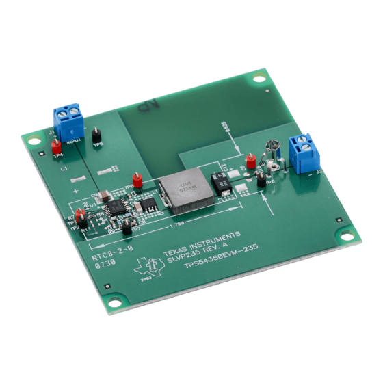
Input/Output Connections 2.1 Input/Output Connections The TPS54350EVM−235 has the following two input/output connectors: V (J1), and V (J3). A diagram showing the connection points is shown in Figure 2−1. A power supply capable of supplying 5 A should be connected to J1 through a pair of 20 AWG wires. -
Page 16: Efficiency
Efficiency 2.2 Efficiency The TPS54350EVM−235 efficiency peaks at load current of about 1 A and V of 6 V, and then decreases as the load current increases towards full load. For higher input voltages, quiescent losses are greater and the efficiency peaks under full load conditions. -
Page 17: Power Dissipation
Power Dissipation 2.3 Power Dissipation The low junction-to-case thermal resistance of the PWP package, along with a good board layout, allows the TPS54350EVM−235 EVMs to output full rated load current while maintaining safe junction temperatures. With a 12-V input source and a load approaching the current limit of 4.2 A, the junction temperature is approximately 47°C. -
Page 18: Output Voltage Regulation
Output Voltage Regulation 2.4 Output Voltage Regulation The output voltage load regulation of the TPS54350EVM−235 is shown in Figure 2−4, while the output voltage line regulation is shown in Figure 2−5. Measurements are given for an ambient temperature of 25°C. Figure 2−4. -
Page 19: Load Transients
Load Transients 2.5 Load Transients The TPS54350EVM−235 response to load transients is shown in Figure 2−6. The current step is from 25% to 75% of maximum rated load. Total peak-to-peak voltage variation is as shown, including ripple and noise on the output. -
Page 20: Loop Characteristics
Loop Characteristic 2.6 Loop Characteristic The TPS54350EVM−235 loop response characteristics are shown in Figure 2−7 and Figure 2−8. Gain and phase plots are shown for each device at minimum and maximum operating voltage. Figure 2−7. Measured Loop Response, TPS54350, V = 6 V MEASURED LOOP RESPONSE Phase... -
Page 21: Output Voltage Ripple
Output Voltage Ripple 2.7 Output Voltage Ripple The TPS54350EVM−235 output voltage ripple is shown in Figure 2−9. The input voltage is 3.3 V for the TPS54350. Output current is the rated full load of 3 A. Voltage is measured directly across output capacitors. Figure 2−9. -
Page 22: Gate Drive
Gate Drive 2.9 Gate Drive The TPS54350 provides the the gate drive signal for a synchronous low-side FET. This gate drive signal and its relation ship to the PHASE signal is shown in Figure 2−11. Figure 2−11. Gate Drive Signal, TPS54350 LSG 5 V/div V phase 5 V/div t −... -
Page 23: Powering Up And Down
Powering Up and Down 2.10 Powering Up and Down The start-up voltage waveform of the TPS54350EVM−235 is shown in Figure 2−12. The waveform shows the nominal 12-V input voltage in Ch. 1, the 3.3-V output ramping up in Ch. 2 and the PWRGD signal in Ch. 3. Note that the PWRGD signal is pulled up externally to 3.3 V. -
Page 24: Board Layout
Chapter 3 Board Layout This chapter provides a description of the TPS54350EVM−235 board layout and layer illustrations. Topic Page Layout ............Board Layout... -
Page 25: Layout
Layout 3.1 Layout The board layout for the TPS54350EVM−235 is shown in Figure 3−1 through Figure 3−4. The topside layer of the TPS54350EVM−235 is laid out in a manner typical of a user application that is optimized for small size. The top and bottom layers are 1.5 oz. -
Page 26: Bottom Side Layout
Layout Figure 3−2. Bottom Side Layout Figure 3−3. Top Side Assembly Board Layout... -
Page 27: Bottom Side Assembly
Layout Figure 3−4. Bottom Side Assembly... -
Page 28: Schematic And Bill Of Materials
Chapter 4 Schematic and Bill of Materials The TPS54350EVM−235 schematic and bill of materials are presented in this chapter. Topic Page Schematic ........... . Bill of Materials . -
Page 29: Schematic
Schematic 4.1 Schematic The schematic for the TPS54350EVM−235 is shown in Figure 4−1. Figure 4−1. TPS54350EVM-235 Schematic... -
Page 30: Bill Of Materials
Bill of Materials 4.2 Bill of Materials The bill of materials for the TPS54350EVM−235 is given by Table 4−1. TPS54350EVM-235 Bill of Materials Count Ref Des Description Size Part Number Capacitor, aluminum, 100 µF, 35 V, 20%, FC − 0.335 x 0.374 Panasonic EEVFC1V101P Series... - Page 32 Mouser Electronics Authorized Distributor Click to View Pricing, Inventory, Delivery & Lifecycle Information: Texas Instruments TPS54350EVM-235...
Need help?
Do you have a question about the SWIFT TPS54350EVM-235 and is the answer not in the manual?
Questions and answers