Table of Contents
Advertisement
Quick Links
www.ti.com
User's Guide
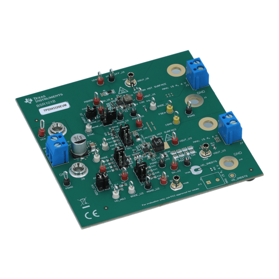
TPS543320 SWIFT™ Step-Down Converter Evaluation
Module User's Guide
This user's guide contains information for the TPS543320EVM evaluation module (BSR101) and the
TPS543320 dc/dc converter. Also included are the performance characteristics, schematic, and bill of materials
for the TPS543320EVM.
1
Introduction.............................................................................................................................................................................3
1.1 Background........................................................................................................................................................................
1.2 Before You Begin...............................................................................................................................................................
1.3 Performance Characteristics Summary.............................................................................................................................
Modifications.........................................................................................................................................6
2.1 Output Voltage...................................................................................................................................................................
2.2 Switching Frequency (FSEL Pin).......................................................................................................................................
2.3 Current Limit, Soft-Start Time, and Internal Compensation (MODE Pin)...........................................................................
UVLO................................................................................................................................................................7
3 Test Setup and Results..........................................................................................................................................................
3.1 Input/Output Connections..................................................................................................................................................
3.2 Efficiency..........................................................................................................................................................................
3.3 Output Voltage Regulation...............................................................................................................................................
3.4 Load Transient and Loop Response................................................................................................................................
3.5 Output Voltage Ripple......................................................................................................................................................
3.6 Input Voltage Ripple.........................................................................................................................................................
Clock..................................................................................................................................................18
3.8 Start-up and Shutdown with EN.......................................................................................................................................
3.9 Start-up and Shutdown with VIN......................................................................................................................................
Limit.......................................................................................................................................................21
3.11 Overvoltage Protection...................................................................................................................................................
3.12 Thermal Performance....................................................................................................................................................
Layout.........................................................................................................................................................................24
4.1 Layout..............................................................................................................................................................................
Materials...........................................................................................................................................25
5.1 Schematic........................................................................................................................................................................
Materials.................................................................................................................................................................28
6 Revision History...................................................................................................................................................................
Regulation.................................................................................................................................................13
Regulation..................................................................................................................................................13
Response...........................................................................................................................................14
Response.........................................................................................................................................14
Plot..........................................................................................................................................................14
Figure 3-12. U2 Bode Plot.........................................................................................................................................................
Figure 3-14. U2 Loop Phase with Different Ramp Settings.......................................................................................................
Figure 3-15. U1 Output Ripple - No Load.................................................................................................................................
Figure 3-16. U1 Output Ripple - 3-A Load................................................................................................................................
SLVUC07A - DECEMBER 2020 - REVISED MAY 2021
Submit Document Feedback
ABSTRACT
Table of Contents
List of Figures
Settings..........................................................................................................15
TPS543320 SWIFT™ Step-Down Converter Evaluation Module User's Guide
Copyright © 2021 Texas Instruments Incorporated
Table of Contents
3
3
4
6
7
7
8
8
11
13
14
16
17
19
20
22
23
24
26
30
14
15
16
16
1
Advertisement
Table of Contents

Related Manuals for Texas Instruments TPS543320EVM


Summary of Contents for Texas Instruments TPS543320EVM
-
Page 1: Table Of Contents
TPS543320 SWIFT™ Step-Down Converter Evaluation Module User's Guide ABSTRACT This user’s guide contains information for the TPS543320EVM evaluation module (BSR101) and the TPS543320 dc/dc converter. Also included are the performance characteristics, schematic, and bill of materials for the TPS543320EVM. Table of Contents Introduction.....................................3... - Page 2 Figure 5-2. U2 Schematic................................List of Tables Table 1-1. Input Voltage and Output Current Summary.......................3 Table 1-2. TPS543320EVM Small Size (U1) Performance Characteristics Summary..............Table 1-3. TPS543320EVM High Efficiency (U2) Performance Characteristics Summary............5 Table 2-1. VOUT Selection................................Table 2-2. FSEL Selection................................
-
Page 3: Introduction
The following warnings and cautions are noted for the safety of anyone using or working close to the TPS543320EVM. Observe all safety precautions. The TPS543320EVM may become hot during operation due to dissipation of power in some operating conditions. Avoid contact with the board. Follow all applicable Warning safety procedures applicable to your laboratory. -
Page 4: Performance Characteristics Summary
Introduction www.ti.com 1.3 Performance Characteristics Summary A summary of the TPS543320EVM performance characteristics is provided in Table 1-2 Table 1-3. The TPS543320EVM is designed and tested for V = 4 V to 18 V. Characteristics are given for an input voltage of = 12 V and output voltages of 1.8 V and 3.3 V, unless otherwise specified. -
Page 5: Table 1-3. Tps543320Evm High Efficiency (U2) Performance Characteristics
Introduction Table 1-3. TPS543320EVM High Efficiency (U2) Performance Characteristics Summary SPECIFICATION TEST CONDITIONS UNIT voltage range = 12 V, I = 0 A 21.8 Input current = 5 V, I = 3 A start voltage Set by EN pin resistor divider 4.53... -
Page 6: Configurations And Modifications
3.3 V 7 to 8 pin shorted (R26+R20)||R21 = 2.54 kΩ 5.0 V Default Setting TPS543320 SWIFT™ Step-Down Converter Evaluation Module User's Guide SLVUC07A – DECEMBER 2020 – REVISED MAY 2021 Submit Document Feedback Copyright © 2021 Texas Instruments Incorporated... -
Page 7: Switching Frequency (Fsel Pin)
In the U1 design, the EN pin is floating, so only the internal UVLO of the device is used. SLVUC07A – DECEMBER 2020 – REVISED MAY 2021 TPS543320 SWIFT™ Step-Down Converter Evaluation Module User's Guide Submit Document Feedback Copyright © 2021 Texas Instruments Incorporated... -
Page 8: Test Setup And Results
U2 with TP17 as the ground reference. If modifications are made to the TPS543320EVM, the input current may change. The input power supply and wires connecting the EVM to the power supply must be rated for the input current. -
Page 9: Table 3-1. Connectors And Jumpers
2-2. MODE Select MODE selection header. Use shunt to select MODE resistor. See Table 2-3. SLVUC07A – DECEMBER 2020 – REVISED MAY 2021 TPS543320 SWIFT™ Step-Down Converter Evaluation Module User's Guide Submit Document Feedback Copyright © 2021 Texas Instruments Incorporated... -
Page 10: Table 3-2. Test Points
TP33 PGND Both PGND test point for load transient circuit TP34 MODE MODE test point TPS543320 SWIFT™ Step-Down Converter Evaluation Module User's Guide SLVUC07A – DECEMBER 2020 – REVISED MAY 2021 Submit Document Feedback Copyright © 2021 Texas Instruments Incorporated... -
Page 11: Efficiency
3.2 Efficiency Figure 3-1 through Figure 3-4 show the efficiency for both designs on the TPS543320EVM. Using the selection jumpers for U2, the results for different output voltage and switching frequency combinations are included. The test points listed in Table 3-3 are used for the efficiency measurement. - Page 12 = 9 V = 3.3 V Figure 3-4. U2 Efficiency – 3.3-V Output with Different Switching Frequencies TPS543320 SWIFT™ Step-Down Converter Evaluation Module User's Guide SLVUC07A – DECEMBER 2020 – REVISED MAY 2021 Submit Document Feedback Copyright © 2021 Texas Instruments Incorporated...
-
Page 13: Output Voltage Regulation
= 18 V 17 18 Figure 3-8. U2 Line Regulation Figure 3-7. U2 Load Regulation SLVUC07A – DECEMBER 2020 – REVISED MAY 2021 TPS543320 SWIFT™ Step-Down Converter Evaluation Module User's Guide Submit Document Feedback Copyright © 2021 Texas Instruments Incorporated... -
Page 14: Load Transient And Loop Response
U1 and TP29 for U2. When using the load transient circuit included on the TPS543320EVM, slowly increase amplitude of function generator for desired load step amplitude then vary the rise and fall times for the desired slew rate. The current for the load step can be sensed with the ISNS test point. -
Page 15: Figure 3-13. U2 Loop Gain With Different Ramp Settings
Figure 3-14. U2 Loop Phase with Different Ramp Figure 3-13. U2 Loop Gain with Different Ramp Settings Settings SLVUC07A – DECEMBER 2020 – REVISED MAY 2021 TPS543320 SWIFT™ Step-Down Converter Evaluation Module User's Guide Submit Document Feedback Copyright © 2021 Texas Instruments Incorporated... -
Page 16: Output Voltage Ripple
Figure 3-15 through Figure 3-18 show the TPS543320EVM output voltage ripple. The load currents are no load and 3 A. V = 12 V. The VOUT voltage is measured using TP10 for U1 and TP29 for U2. Figure 3-15. U1 Output Ripple – No Load Figure 3-16. -
Page 17: Input Voltage Ripple
Figure 3-19 through Figure 3-22 show the TPS543320EVM input voltage ripple. The load currents are no load and 3 A. V = 12 V. The ripple voltage is measured across C1 for U1 and measured across C13 for U2. Figure 3-19. U1 Input Ripple – No Load Figure 3-20. -
Page 18: Synchronizing To A Clock
Figure 3-23. U1 and U2 Synchronized to a Clock Figure 3-24. U2 Clock Synchronization Transitions TPS543320 SWIFT™ Step-Down Converter Evaluation Module User's Guide SLVUC07A – DECEMBER 2020 – REVISED MAY 2021 Submit Document Feedback Copyright © 2021 Texas Instruments Incorporated... -
Page 19: Start-Up And Shutdown With En
Figure 3-26. U2 Shutdown with EN – No Load Figure 3-27. U2 Startup with EN – No Load and Measuring BP5 SLVUC07A – DECEMBER 2020 – REVISED MAY 2021 TPS543320 SWIFT™ Step-Down Converter Evaluation Module User's Guide Submit Document Feedback Copyright © 2021 Texas Instruments Incorporated... -
Page 20: Start-Up And Shutdown With Vin
Figure 3-28. U2 Start-up with VIN – 1.5-A Load Figure 3-29. U2 Shutdown with VIN – 1.5-A Load TPS543320 SWIFT™ Step-Down Converter Evaluation Module User's Guide SLVUC07A – DECEMBER 2020 – REVISED MAY 2021 Submit Document Feedback Copyright © 2021 Texas Instruments Incorporated... -
Page 21: Hiccup Current Limit
Figure 3-31. U2 OCP Hiccup and Recover Figure 3-30. U2 Output Overcurrent Protection – Overload SLVUC07A – DECEMBER 2020 – REVISED MAY 2021 TPS543320 SWIFT™ Step-Down Converter Evaluation Module User's Guide Submit Document Feedback Copyright © 2021 Texas Instruments Incorporated... -
Page 22: Overvoltage Protection
OVP fault is cleared. It does not wait for the hiccup time period. Figure 3-32. U2 Overvoltage Protection Figure 3-33. U2 OVP and Recover TPS543320 SWIFT™ Step-Down Converter Evaluation Module User's Guide SLVUC07A – DECEMBER 2020 – REVISED MAY 2021 Submit Document Feedback Copyright © 2021 Texas Instruments Incorporated... -
Page 23: Thermal Performance
Figure 3-36. U1 Thermal Performance – Both 3-A Figure 3-37. U2 Thermal Performance – Both 3-A Load Load SLVUC07A – DECEMBER 2020 – REVISED MAY 2021 TPS543320 SWIFT™ Step-Down Converter Evaluation Module User's Guide Submit Document Feedback Copyright © 2021 Texas Instruments Incorporated... -
Page 24: Board Layout
Board Layout www.ti.com 4 Board Layout This section provides a description of the TPS543320EVM board layout and layer illustrations. 4.1 Layout The board layout for the TPS543320EVM is shown in Figure 4-1 through Figure 4-6. The top-side layer of the EVM is laid out in a manner typical of a user application. -
Page 25: Schematic And Bill Of Materials
Figure 4-5. Mid Layer 2 Layout Figure 4-6. Bottom Layer Layout 5 Schematic and Bill of Materials This section presents the TPS543320EVM schematic and bill of materials. SLVUC07A – DECEMBER 2020 – REVISED MAY 2021 TPS543320 SWIFT™ Step-Down Converter Evaluation Module User's Guide Submit Document Feedback Copyright ©... -
Page 26: Schematic
U1. Figure 5-2 is the schematic for U2. Figure 5-1. U1 Schematic TPS543320 SWIFT™ Step-Down Converter Evaluation Module User's Guide SLVUC07A – DECEMBER 2020 – REVISED MAY 2021 Submit Document Feedback Copyright © 2021 Texas Instruments Incorporated... -
Page 27: Figure 5-2. U2 Schematic
Schematic and Bill of Materials Figure 5-2. U2 Schematic SLVUC07A – DECEMBER 2020 – REVISED MAY 2021 TPS543320 SWIFT™ Step-Down Converter Evaluation Module User's Guide Submit Document Feedback Copyright © 2021 Texas Instruments Incorporated... -
Page 28: Bill Of Materials
Schematic and Bill of Materials www.ti.com 5.2 Bill of Materials Table 5-1 presents the bill of materials for the TPS543320EVM. Table 5-1. TPS543320EVM Bill of Materials DESIGNATOR VALUE DESCRIPTION PACKAGE REFERENCE PART NUMBER MANUFACTURER !PCB1 Printed Circuit Board BSR101 BO1, BO2, BO3, BO4 Bumpon, Hemisphere, 0.375 X... - Page 29 Schematic and Bill of Materials Table 5-1. TPS543320EVM Bill of Materials (continued) DESIGNATOR VALUE DESCRIPTION PACKAGE REFERENCE PART NUMBER MANUFACTURER R22, R48 100 k RES, 100 k, 5%, 0.1 W, 0603 0603 CRCW0603100KJNEAC Vishay-Dale 22.1 k RES, 22.1 k, 1%, 0.1 W, 0603...
-
Page 30: Revision History
Revision History www.ti.com Table 5-1. TPS543320EVM Bill of Materials (continued) DESIGNATOR VALUE DESCRIPTION PACKAGE REFERENCE PART NUMBER MANUFACTURER TP25 Test Point, Multipurpose, Red, Red Multipurpose Testpoint 5010 Keystone TP30 Connector, Receptacle, 50 Ω, SMB Connector SMBR004D00 JAE Electronics 6 Revision History NOTE: Page numbers for previous revisions may differ from page numbers in the current version. - Page 31 STANDARD TERMS FOR EVALUATION MODULES Delivery: TI delivers TI evaluation boards, kits, or modules, including any accompanying demonstration software, components, and/or documentation which may be provided together or separately (collectively, an “EVM” or “EVMs”) to the User (“User”) in accordance with the terms set forth herein.
- Page 32 www.ti.com Regulatory Notices: 3.1 United States 3.1.1 Notice applicable to EVMs not FCC-Approved: FCC NOTICE: This kit is designed to allow product developers to evaluate electronic components, circuitry, or software associated with the kit to determine whether to incorporate such items in a finished product and software developers to write software applications for use with the end product.
- Page 33 www.ti.com Concernant les EVMs avec antennes détachables Conformément à la réglementation d'Industrie Canada, le présent émetteur radio peut fonctionner avec une antenne d'un type et d'un gain maximal (ou inférieur) approuvé pour l'émetteur par Industrie Canada. Dans le but de réduire les risques de brouillage radioélectrique à...
- Page 34 www.ti.com EVM Use Restrictions and Warnings: 4.1 EVMS ARE NOT FOR USE IN FUNCTIONAL SAFETY AND/OR SAFETY CRITICAL EVALUATIONS, INCLUDING BUT NOT LIMITED TO EVALUATIONS OF LIFE SUPPORT APPLICATIONS. 4.2 User must read and apply the user guide and other available documentation provided by TI regarding the EVM prior to handling or using the EVM, including without limitation any warning or restriction notices.
- Page 35 Notwithstanding the foregoing, any judgment may be enforced in any United States or foreign court, and TI may seek injunctive relief in any United States or foreign court. Mailing Address: Texas Instruments, Post Office Box 655303, Dallas, Texas 75265 Copyright © 2019, Texas Instruments Incorporated...
- Page 36 TI products. TI’s provision of these resources does not expand or otherwise alter TI’s applicable warranties or warranty disclaimers for TI products.IMPORTANT NOTICE Mailing Address: Texas Instruments, Post Office Box 655303, Dallas, Texas 75265 Copyright © 2021, Texas Instruments Incorporated...
Need help?
Do you have a question about the TPS543320EVM and is the answer not in the manual?
Questions and answers