Table of Contents
Advertisement
Quick Links
Advertisement
Table of Contents

Related Manuals for Fibocom SU806 Series


Summary of Contents for Fibocom SU806 Series
- Page 1 FIBOCOM SU806 Series Hardware Guide Version: V2.0.0 Date: 2021-02-01...
- Page 2 16GB e.MMC+16Gb LPDDR3.SDRAM, 4G frequency, Android 10, SU806-CN-10 applicable to China 8GB e.MMC+8Gb LPDDR3.SDRAM, 4G frequency, Android 10, SU806-EAU-00 applicable to Eurasian Reproduction forbidden without Fibocom Wireless Inc. written authorization - All Rights Reserved. FIBOCOM SU806 Series Hardware Guide Page 2 of 91...
- Page 3 Trademark The trademark is registered and owned by Fibocom Wireless Inc. Reproduction forbidden without Fibocom Wireless Inc. written authorization - All Rights Reserved. FIBOCOM SU806 Series Hardware Guide Page 3 of 91...
- Page 4 Mo Xiaoke Tu Min V2.0.0 Chen Guojiang 2021-02-01 function based on SU806 He Sihai Li Xiyi Series Hardware Guide v1.0.2 Reproduction forbidden without Fibocom Wireless Inc. written authorization - All Rights Reserved. FIBOCOM SU806 Series Hardware Guide Page 4 of 91...
-
Page 5: Table Of Contents
GPIO .......................... 39 C ..........................41 3.10 RBG ........................... 42 3.11 ADC ..........................42 3.12 Battery Power Supply Interface .................. 43 Reproduction forbidden without Fibocom Wireless Inc. written authorization - All Rights Reserved. FIBOCOM SU806 Series Hardware Guide Page 5 of 91... - Page 6 RF PCB Layout Design Guide ..................65 WIFI and Bluetooth ......................67 WIFI Overview ......................67 WIFI Performance ...................... 67 Bluetooth Overview ....................68 Reproduction forbidden without Fibocom Wireless Inc. written authorization - All Rights Reserved. FIBOCOM SU806 Series Hardware Guide Page 6 of 91...
- Page 7 Appendix B GPRS Encoding Scheme ................89 Appendix C GPRS Multislot ....................90 Appendix D EDGE Modulation and Encoding Method ...........91 Reproduction forbidden without Fibocom Wireless Inc. written authorization - All Rights Reserved. FIBOCOM SU806 Series Hardware Guide Page 7 of 91...
-
Page 8: Introduction
This document describes the electrical characteristics, RF performance, structure size, application environment, etc. of SU806 series module. With the assistance of the document and other instructions, the developers can quickly understand the hardware functions of the SU806 series module and develop products. -
Page 9: Related Document
This exterior label Reproduction forbidden without Fibocom Wireless Inc. written authorization - All Rights Reserved. FIBOCOM SU806 Series Hardware Guide... - Page 10 There is requirement that the grantee provide guidance to the host manufacturer for compliance with Part 15B requirements. Hereby, Fibocom Wireless Inc. declares that the radio equipment type SU806-EAU is in compliance with Directive 2014/53/EU. Reproduction forbidden without Fibocom Wireless Inc. written authorization - All Rights Reserved.
-
Page 11: Product Overview
WIFI/BT short-distance radio transmission technology, as well as GNSS wireless positioning technology. SU806 series module is embedded with Android operating system and support various interfaces such as MIPI/USB/UART/SPI/I2C. It is the optimal solution for the core system of wireless smart products. Its... -
Page 12: Product Specification
2.2 Product Specification SU806 series module is available in 262 LCC+LGA package that includes 146 LCC pins and 116 LGA pins. The dimension is 40.5mm×40.5mm×2.8mm. It can be embedded in various M2M applications. It is suitable for the development of smart devices such as smart POS, cash registers, robots, UAVs, smart homes, security monitoring and multimedia terminals. - Page 13 Support dual (U)SIM dual standby single pass, support hot plug (closed by default) UART interface Three UART serial interfaces Reproduction forbidden without Fibocom Wireless Inc. written authorization - All Rights Reserved. FIBOCOM SU806 Series Hardware Guide Page 13 of 91...
-
Page 14: Functional Block Diagram
When the module is operating within this temperature range, the functions of it are normal and the relevant performance meets the 3GPP standard. 2.3 Functional Block Diagram Functional diagram shows the main hardware features of the SU806 series module: Baseband ... - Page 15 Interface Memory RESET Baseband PWRKEY Multimedia Connectivity SDIO GPIO USB VoL key UART (U)SIM Figure 2-1 Functional block diagram Reproduction forbidden without Fibocom Wireless Inc. written authorization - All Rights Reserved. FIBOCOM SU806 Series Hardware Guide Page 15 of 91...
-
Page 16: Pin Definition
Note: “NC” represent No Connect, the pin of this position is reserved and does not need to be connected. Reproduction forbidden without Fibocom Wireless Inc. written authorization - All Rights Reserved. FIBOCOM SU806 Series Hardware Guide Page 16 of 91... -
Page 17: Pin Descriptions
Input/Output Digital Input Digital Output Power Input Power Output Analog Input Analog Output Open Drain Pin descriptions of SU806 series module are presented in the following table: Table 2-5 Pin description Pin Name Functional Description Note Number Power supply 1,2,145,1... - Page 18 Active low KEY_PWR_ON Power key 1 Active low Active low, support two key(KEY_PWR_ON& KEY_RESIN_N Reset key KEY_RESIN_N)reset and one key(KEY_PWR_ON) Reproduction forbidden without Fibocom Wireless Inc. written authorization - All Rights Reserved. FIBOCOM SU806 Series Hardware Guide Page 18 of 91...
- Page 19 SD card clock I2C interface SENSOR_I2C_SCL I2C clock For sensor by default SENSOR_I2C_SDA I2C data For sensor by default Reproduction forbidden without Fibocom Wireless Inc. written authorization - All Rights Reserved. FIBOCOM SU806 Series Hardware Guide Page 19 of 91...
- Page 20 UART2_TX UART2 data transmission Reserved UART2_RX UART2 data reception Reserved SPI interface SPI_CLK SPI clock SPI_CS SPI chip selects Reproduction forbidden without Fibocom Wireless Inc. written authorization - All Rights Reserved. FIBOCOM SU806 Series Hardware Guide Page 20 of 91...
- Page 21 LCD TP reset signal Camera interface MIPI_CSI0_CLK_P MIPI rear camera serial interface clock MIPI_CSI0_CLK_N MIPI_CSI0_LN0_P MIPI rear camera serial interface lane MIPI_CSI0_LN0_N Reproduction forbidden without Fibocom Wireless Inc. written authorization - All Rights Reserved. FIBOCOM SU806 Series Hardware Guide Page 21 of 91...
- Page 22 MIPI depth camera serial interface lane MIPI_CSI1_LN2_P DCAM_MCLK Depth camera master clock DCAM_RST Depth camera reset signal DCAM_PWDN Depth camera power down Reproduction forbidden without Fibocom Wireless Inc. written authorization - All Rights Reserved. FIBOCOM SU806 Series Hardware Guide Page 22 of 91...
- Page 23 WIFI/BT antenna ANT_GNSS GNSS antenna Interrupt interface Ambient light sensor and ALPS_INT_N proximity sensor interrupt MAG_RST Magnetic sensor reset Reproduction forbidden without Fibocom Wireless Inc. written authorization - All Rights Reserved. FIBOCOM SU806 Series Hardware Guide Page 23 of 91...
- Page 24 General Purpose Input and GPIO_131 INPUT(WPD) Output.1.8V power domain GPIO_130 INPUT(WPD) GPIO_133 INPUT(WPD) GPIO_132 INPUT(WPD) GPIO_121 OUTPUT GPIO_138 INPUT(WPU) Reproduction forbidden without Fibocom Wireless Inc. written authorization - All Rights Reserved. FIBOCOM SU806 Series Hardware Guide Page 24 of 91...
- Page 25 GPIO_11 INPUT(WPD) GPIO_7 INPUT(WPD) GPIO_143 INPUT(WPU) GPIO_10 INPUT(WPD) GPIO_141 INPUT(WPU) GPIO_26 INPUT(WPD) GPIO_22 INPUT(WPD) GPIO_23 INPUT(WPD) Reproduction forbidden without Fibocom Wireless Inc. written authorization - All Rights Reserved. FIBOCOM SU806 Series Hardware Guide Page 25 of 91...
- Page 26 The GPIOs with “WPU” aren’t recommended as the enable control of default highly efficient devices. For example, backlight enable of LCM and audio amplifier enable. Reproduction forbidden without Fibocom Wireless Inc. written authorization - All Rights Reserved. FIBOCOM SU806 Series Hardware Guide...
-
Page 27: Application Interface
3 Application Interface 3.1 Power Supply The SU806 series module provides four VBAT pins for connecting to external power supply source. The input range of power is 3.5V to 4.2V and the recommended value is 3.8V. The performance of the power supply such as its load capacity, ripple etc. -
Page 28: Vrtc
The VRTC parameters are as follows: Table 3-3 VRTC parameters Parameter Minimum Typical Maximum Unit VRTC output voltage 3.35 Reproduction forbidden without Fibocom Wireless Inc. written authorization - All Rights Reserved. FIBOCOM SU806 Series Hardware Guide Page 28 of 91... -
Page 29: Power Output
Coin cell Figure 3-3 VRTC reference design 3.1.3 Power Output The SU806 series module provides multiple power outputs for peripheral circuits. It is recommended to connect 33pF and 10pF capacitors in parallel with every power to avoid high frequency interference effectively. -
Page 30: Control Signal
VIB_DRV_N 1.8-3.3 3.2 Control Signal 3.2.1 Power on/off SU806 series module provides one-way power on/off control signal to module’s power on/off, restart and sleep/wake up. Its pin definition is shown as follow table: Table 3-5 Power on/off signal Pin Name... -
Page 31: Power Off
3.2.1.3 Sleep/Wake up When module in standby mode, pull down KEY_PWR_ON pin 0.1s~0.5s and then release it, module will Reproduction forbidden without Fibocom Wireless Inc. written authorization - All Rights Reserved. FIBOCOM SU806 Series Hardware Guide Page 31 of 91... -
Page 32: Reset
3.3 USB The SU806 series module supports one USB 2.0 interface; USB2.0 supports HS (480Mbps) modes and compatible USB1.1 FS (12Mbps). USB supports OTG function (need 5V external power supply); Its pin definition is shown in the following table: Reproduction forbidden without Fibocom Wireless Inc. - Page 33 The reference design of USB2.0 is show as follow figure: Connector Module VBUS USB_VBUS USB_DM USB_DP USB_ID Figure 3-8 USB2.0 reference design Reproduction forbidden without Fibocom Wireless Inc. written authorization - All Rights Reserved. FIBOCOM SU806 Series Hardware Guide Page 33 of 91...
- Page 34 Table 3-7 Length of USB differential signal line in module Pin Name Length (mm) Length Difference (DP-DM) mm Number 11.33134 USB_DP 0.40037 10.93097 USB_DM Reproduction forbidden without Fibocom Wireless Inc. written authorization - All Rights Reserved. FIBOCOM SU806 Series Hardware Guide Page 34 of 91...
-
Page 35: Uart
3.4 UART SU806 series module defines three UART ports,all are 1.8V voltage domain ,the function of UART2 has not achieve at present. Its pin definition is shown in the following table: Table 3-8 UART interface pin definition Pin Name Pin Number... -
Page 36: Spi
Figure 3-11 Level shift reference design 2 3.5 SPI SU806 series module provides one master only SPI interface, the pin definition is shown in the following table: Table 3-9 SPI pin definition... -
Page 37: U)Sim
SPI master input slave output SPI_MOSI SPI master output slave input 3.6 (U)SIM The SU806 series module supports two (U)SIM cards, dual-SIM dual-standby single-active (default double) and both support hot plug (default off). Table 3-10 (U)SIM pin definition Pin Name... -
Page 38: Sdio
3) The decoupling capacitors of the (U)SIM card signal and the ESD device should be placed close to the card holder. 3.7 SDIO SU806 series module supports one SDIO interface. The pin definition is shown in the following table: Table 3-11 SDIO pin definition Pin Name... -
Page 39: Gpio
3) Pull up SD_DET with VDD1V85. 4) SDIO is a high-speed digital signal cable, needs to be shielded. 3.8 GPIO SU806 series module have rich GPIOs and the interface level is 1.8V. The pin definition is shown in the following table: Table 3-12 GPIO list Reproduction forbidden without Fibocom Wireless Inc. - Page 40 INPUT(WPU) GPIO_140 INPUT(WPU) GPIO_88 INPUT(WPU) GPIO_30 INPUT(WPD) GPIO_29 INPUT(WPD) GPIO_27 INPUT(WPD) GPIO_85 OUTPUT GPIO_154 INPUT(WPD) INPUT(WPD) GPIO_155 GPIO_28 INPUT(WPD) Reproduction forbidden without Fibocom Wireless Inc. written authorization - All Rights Reserved. FIBOCOM SU806 Series Hardware Guide Page 40 of 91...
-
Page 41: I 2 C
WPD: Weak pull down 3.9 I SU806 series module provides four I2C interfaces for TP, camera, sensor, etc. And four I2C interfaces are all internal pull up, when in use, please reserve pull-up resistors to 1.8V power domain. The pin definition... -
Page 42: Rbg
When I2C has more than one peripheral, please ensure the uniqueness of every peripheral address. 3.10 RBG SU806 series module provides three RGB LED inputs, its pin definition is shown in the following table: Table 3-14 RGB pin definition Pin Name... -
Page 43: Battery Power Supply Interface
3.12 Battery Power Supply Interface SU806 series module just support circuit modes coulomb counter fuel gauge, if use coulomb counter IC externally, please connect SENSE_P and SENSE_N pin to GND. Table 3-16 Battery power supply pin definition Pin Name Pin Num... -
Page 44: Charge Enable Interface
Vibration motor driver output connect with Vibration motor + 3.15 LCM The video output of SU806 series module can support single-screen display. Its screen interface is based on MIPI_DSI standard and supports 4 sets of high-speed differential data transmit, and supports HD+ maximum. - Page 45 MIPI_DSI_LN2_N MIPI_D2N MIPI_D1P MIPI_DSI_LN1_P MIPI_DSI_LN1_N MIPI_D1N MIPI_CLKP MIPI_DSI_CLK_P MIPI_CLKN MIPI_DSI_CLK_N MIPI_D0P MIPI_DSI_LN0_P MIPI_DSI_LN0_N MIPI_D0N Figure 3-15 LCM reference design Reproduction forbidden without Fibocom Wireless Inc. written authorization - All Rights Reserved. FIBOCOM SU806 Series Hardware Guide Page 45 of 91...
- Page 46 63.44691 MIPI_DSI0_LN3_P 3.16 TP SU806 series module provides one I2C interface can be used to connect the touch panel and it provides Reproduction forbidden without Fibocom Wireless Inc. written authorization - All Rights Reserved. FIBOCOM SU806 Series Hardware Guide Page 46 of 91...
-
Page 47: Camera
13MP. The pin definition of camera interface is shown in the following table: Table 3-22 Camera interface pin definition Pin Name 4-Lane+2-Lane+1-Lane Note Number Reproduction forbidden without Fibocom Wireless Inc. written authorization - All Rights Reserved. FIBOCOM SU806 Series Hardware Guide Page 47 of 91... - Page 48 MIPI front camera serial interface clock + MIPI_CSI1_CLK_P MIPI front camera serial interface lane 0 - MIPI_CSI1_LN0_N MIPI front camera serial interface lane 0 + Reproduction forbidden without Fibocom Wireless Inc. written authorization - All Rights Reserved. FIBOCOM SU806 Series Hardware Guide Page 48 of 91...
-
Page 49: Rear Camera
DO Front/depth camera I2C clock CAM_I2C_SDA1 Front/depth camera I2C data 3.17.1 Rear Camera Reference design of rear camera is shown as follows: Reproduction forbidden without Fibocom Wireless Inc. written authorization - All Rights Reserved. FIBOCOM SU806 Series Hardware Guide Page 49 of 91... -
Page 50: Front Camera
CAM_I2C_SDA1 CLK_P MIPI_CSI1_CLK_P CLK_N MIPI_CSI1_CLK_N DAT0_P MIPI_CSI1_LN0_P MIPI_CSI1_LN0_N DAT0_N DAT1_P MIPI_CSI1_LN1_P MIPI_CSI1_LN1_N DAT1_N Figure 3-18 Front camera reference design Reproduction forbidden without Fibocom Wireless Inc. written authorization - All Rights Reserved. FIBOCOM SU806 Series Hardware Guide Page 50 of 91... -
Page 51: Depth Camera
10) If two cameras share the same I2C interface, please confirm the I2C addresses of the two cameras do not conflict; Reproduction forbidden without Fibocom Wireless Inc. written authorization - All Rights Reserved. FIBOCOM SU806 Series Hardware Guide Page 51 of 91... - Page 52 MIPI_CSI1_LN0_P -0.10242 11.33166 MIPI_CSI1_LN0_N 11.73285 MIPI_CSI1_LN1_P 0.28125 11.4516 MIPI_CSI1_LN1_N 19.19065 MIPI_CSI1_LN2_P -0.18467 19.37532 MIPI_CSI1_LN2_N 19.95271 MIPI_CSI1_LN3_P 0.07975 19.87296 MIPI_CSI1_LN3_N Reproduction forbidden without Fibocom Wireless Inc. written authorization - All Rights Reserved. FIBOCOM SU806 Series Hardware Guide Page 52 of 91...
-
Page 53: Sensor
ACCL_INT Accelerometer sensor interrupt 3.19 Audio 3.19.1 Audio Interface Pin Definition SU806 series module supports analog audio, have 3 input and 3 output. Pin definition is shown in the following table: Table 3-25 Audio interface pin definition Pin Name Description... - Page 54 Sub-mic input Design notice: 1) SU806 series module has MIC bias circuit internally, and no external addition is required. 2) The SPK is configured as class D amplifier output, cannot connect with amplifier externally, it is recommended to connect 8Ω speakers. Note that the route width must meet the power rating requirements;...
-
Page 55: Microphone Circuit Design
MIC_P MIC_M Figure 3-20 Microphone reference design 3.19.3 Earpiece Circuit Design Module EAR_P EAR_M Figure 3-21 Earpiece reference design Reproduction forbidden without Fibocom Wireless Inc. written authorization - All Rights Reserved. FIBOCOM SU806 Series Hardware Guide Page 55 of 91... -
Page 56: Headset Circuit Design
Please choose bidirectional TVS for headset ESD protection. 3.19.5 Speaker Circuit Design Module SPK_P SPK_M Figure 3-23 Speaker reference design Reproduction forbidden without Fibocom Wireless Inc. written authorization - All Rights Reserved. FIBOCOM SU806 Series Hardware Guide Page 56 of 91... -
Page 57: Force Download Interface
3.20 Force Download Interface SU806 series module provides KEY_FORCE_BOOT pin as an emergency download interface. Connect the KEY_FORCE_BOOT with GND when power on, the module can enter the emergency download mode which is used for the final processing mode when the product fails to power on or run normally. To facilitate the subsequent software upgrade and product debugging, please reserve the test pin of this pin. -
Page 58: Antenna Interface
SU806 series module support 2/3/4G main antenna/diversity reception antenna, WIFI/BT antenna and GNSS antenna. 4.1 MAIN/DRX Antenna SU806 series module provides two 2G/3G/4G antenna interfaces. The ANT_MIAN is used to receive and transmit RF signal, the ANT_DRX is used for diversity reception. Table 4-1 Main/DRX pin definition... - Page 59 832-862 Band 28 703-748 758-803 Band 38 2570-2620 2570-2620 LTE TDD Band 40 2300-2400 2300-2400 Band 41 2496-2690 2496-2690 Reproduction forbidden without Fibocom Wireless Inc. written authorization - All Rights Reserved. FIBOCOM SU806 Series Hardware Guide Page 59 of 91...
-
Page 60: Antenna Reference Design
4.1.2 Antenna Reference Design When use the SU806 series module, it is necessary to connect the antenna pin with the RF connector or antenna feed point on the main board via an RF trace. Microstrip trace is recommended for RF trace, with insertion loss within 0.2dB and impedance at 50Ω.A π-type circuit is reserved between the module and... -
Page 61: Wifi/Bt Antenna Reference Design
4.3.2 GNSS Antenna Reference Design 4.3.2.1 Passive Antenna Reference Design: SU806 series module have a built-in LNA. The passive antenna is used in the design of the device. Microstrip trace is recommended for the GNSS RF route, with insertion loss within 0.2dB and impedance at 50Ω. -
Page 62: Active Antenna Reference Design
It is recommended that a high-performance LDO be used to power the antenna. The active antenna reference circuit is shown in the following figure: Reproduction forbidden without Fibocom Wireless Inc. written authorization - All Rights Reserved. FIBOCOM SU806 Series Hardware Guide Page 62 of 91... -
Page 63: Antenna Requirement
33pF ANT_GNSS Figure 4-4 GNSS active antenna reference design 4.4 Antenna Requirement SU806 series module provides four antenna interfaces: main, diversity, WIFI/BT and GNSS. The antenna requirements are as follows: Table 4-8 Antenna requirements SU806 Series Module Antenna Requirement Standard Antenna Requirement VSWR: ≤... - Page 64 VSWR: < 2 (typical) GNSS Passive antenna gain: > 0dBi Active antenna NF: < 15dB (typical) Active antenna gain: > -2dBi Reproduction forbidden without Fibocom Wireless Inc. written authorization - All Rights Reserved. FIBOCOM SU806 Series Hardware Guide Page 64 of 91...
-
Page 65: Rf Pcb Layout Design Guide
Figure 5-1 Two-layer PCB microstrip cable structure Coplanar waveguide entirety structure Figure 5-2 Two-layer PCB coplanar waveguide structure Reproduction forbidden without Fibocom Wireless Inc. written authorization - All Rights Reserved. FIBOCOM SU806 Series Hardware Guide Page 65 of 91... - Page 66 2 times the trace width (2*W). Reproduction forbidden without Fibocom Wireless Inc. written authorization - All Rights Reserved. FIBOCOM SU806 Series Hardware Guide Page 66 of 91...
-
Page 67: Wifi And Bluetooth
6 WIFI and Bluetooth 6.1 WIFI Overview SU806 series module supports 2.4G WLAN wireless communications and 802.11b, 802.11g, 802.11n standards, with a maximum speed up to 72.2Mbps. Its characteristics are as follows: Support Wake-on-WLAN (WoWLAN) Support ad hoc mode ... -
Page 68: Bluetooth Overview
MCS7 6.3 Bluetooth Overview SU806 series module supports BT4.2 (BR/EDR+BLE) standards. The modulation method supports GFSK, 8-DPSK and π/4-DQPSK.BR/EDR. Channel bandwidth is 1MHz and can accommodate 79 channels. The BLE channel bandwidth is 2MHz and can accommodate 40 channels. Its main features are as follows: ... -
Page 69: Gnss
7 GNSS 7.1 Overview SU806 series smart module supports GPS/BeiDou positioning systems. The module is embedded with LNA which can effectively improve the sensitivity of GNSS. 7.2 Performance Test condition:3.8V power supply, environment temperature 25° C Table 7-1 GNSS positioning performance... -
Page 70: Electrical, Reliability And Rf Performance
Storage Temperature 8.2 Absolute Maximum Ratings The functionality of SU806 series module is subject to the absolute maximum/minimum values listed in the following table. Do not exceed these parameters or the part may be damaged permanently. Operation at absolute maximum ratings is not guaranteed. - Page 71 EGPRS data EGPRS-RMS RMS Current DCS1800@ Gamma=5(1UL/4DL) DCS1800@ Gamma=5(4UL/1DL) Band1@ max power WCDMA WCDMA-RMS RMS Current Band8@ max power Reproduction forbidden without Fibocom Wireless Inc. written authorization - All Rights Reserved. FIBOCOM SU806 Series Hardware Guide Page 71 of 91...
- Page 72 EGSM900@ PCL=5 EGSM900@ PCL=19 GSM voice GSM-RMS RMS Current DCS1800@ PCL=0 DCS1800@ PCL=15 GSM voice EGSM900@ PCL=5 2200 GSM-MAX Reproduction forbidden without Fibocom Wireless Inc. written authorization - All Rights Reserved. FIBOCOM SU806 Series Hardware Guide Page 72 of 91...
- Page 73 Power supply, not power on By AT command or select the power off Software power off current menu in LCM selection box Reproduction forbidden without Fibocom Wireless Inc. written authorization - All Rights Reserved. FIBOCOM SU806 Series Hardware Guide Page 73 of 91...
- Page 74 DCS1800@ Gamma=5 (4UL/1DL) Band1@ max power WCDMA WCDMA-RMS RMS Current Band8@ max power FDD data Band1@ max power (10MHz,1RB) LTE-RMS Reproduction forbidden without Fibocom Wireless Inc. written authorization - All Rights Reserved. FIBOCOM SU806 Series Hardware Guide Page 74 of 91...
- Page 75 DPC (Default Paging Cycle)=#256 Radio Off AT+CFUN=4 Flight Mode GSM850@ PCL=5 GSM850@ PCL=19 GSM voice GSM-RMS RMS Current EGSM900@ PCL=5 EGSM900@ PCL=19 Reproduction forbidden without Fibocom Wireless Inc. written authorization - All Rights Reserved. FIBOCOM SU806 Series Hardware Guide Page 75 of 91...
- Page 76 GSM850@ Gamma=6 (4UL/1DL) EGSM900@ Gamma=6 (1UL/4DL) EGPRS data EGPRS-RMS RMS current EGSM900@ Gamma=6 (4UL/1DL) DCS1800@ Gamma=5 (1UL/4DL) DCS1800@ Gamma=5 (4UL/1DL) Reproduction forbidden without Fibocom Wireless Inc. written authorization - All Rights Reserved. FIBOCOM SU806 Series Hardware Guide Page 76 of 91...
-
Page 77: Rf Transmit Power
Band Max Power (dBm) Min Power (dBm) 900 (GMSK) 33± 2 5± 5 1800 (GMSK) 30± 2 0± 5 Reproduction forbidden without Fibocom Wireless Inc. written authorization - All Rights Reserved. FIBOCOM SU806 Series Hardware Guide Page 77 of 91... - Page 78 0± 5 1900 (8PSK) 26.0± 3 0± 5 Band 1 24+1/-3 < -49 WCDMA Band 2 24+1/-3 < -49 Reproduction forbidden without Fibocom Wireless Inc. written authorization - All Rights Reserved. FIBOCOM SU806 Series Hardware Guide Page 78 of 91...
-
Page 79: Rf Receiver Sensitivity
23.0± 2 < -39 8.5 RF Receiver Sensitivity The sensitivity of each frequency band of the SU806 series module is shown in the following table: LTE is Test condition:3.8V power supply, environment temperature 25° C. The test bandwidth of LTE sensitivity 10M, RB configuration please refer to 3GPP standard. - Page 80 -95.8 -94.3 Table 8-11 RF receiver sensitivity of SU806-CN-10 3GPP Mode Band Primary Diversity PRX+Div Unit Requirement -109 -102 Reproduction forbidden without Fibocom Wireless Inc. written authorization - All Rights Reserved. FIBOCOM SU806 Series Hardware Guide Page 80 of 91...
- Page 81 -106.7 Band 2 -104.7 WCDMA Band 5 -104.7 Band 8 -103.7 Band 1 -96.3 LTE FDD Band 3 -93.3 Reproduction forbidden without Fibocom Wireless Inc. written authorization - All Rights Reserved. FIBOCOM SU806 Series Hardware Guide Page 81 of 91...
-
Page 82: Electrostatic Protection
Unit VBAT, GND ± 5 ± 10 Antenna interface ± 4 ± 8 Other interface ± 0.5 ± 1 Reproduction forbidden without Fibocom Wireless Inc. written authorization - All Rights Reserved. FIBOCOM SU806 Series Hardware Guide Page 82 of 91... -
Page 83: Structural Specification
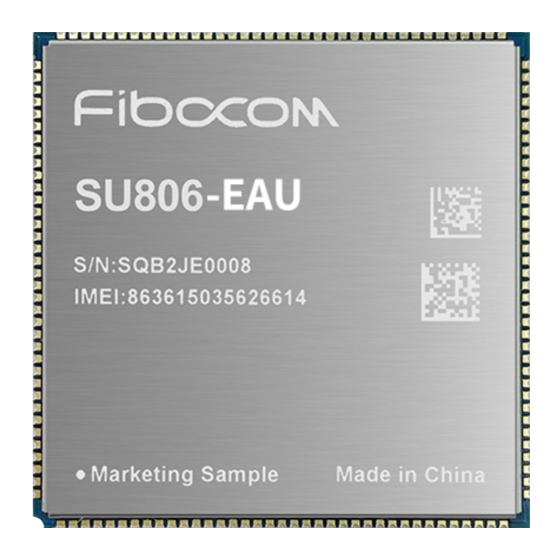
SU806 series module product appearance is shown in the following figure: Figure 9-1 Module product appearance 9.2 Structural Dimension The structural dimension of SU806 series module is shown in the following figure: Figure 9-2 Structural dimension Reproduction forbidden without Fibocom Wireless Inc. written authorization - All Rights Reserved. -
Page 84: Pcb Soldering Pad And Stencil Design
9.3 PCB Soldering Pad and Stencil Design PCB soldering pad and stencil design please refer to FIBOCOM Sx806 Series SMT Design Guide. Reproduction forbidden without Fibocom Wireless Inc. written authorization - All Rights Reserved. FIBOCOM SU806 Series Hardware Guide Page 84 of 91... -
Page 85: Production And Storage
Production and Storage 10.1 SMT SMT production process parameters and related requirements please refer to FIBOCOM Sx806 Series SMT Design Guide. 10.2 Carrier and Storage Carrier and storage please refer to FIBOCOM Sx806 Series SMT Design Guide. Reproduction forbidden without Fibocom Wireless Inc. written authorization - All Rights Reserved. -
Page 86: Appendix A Terms And Acronyms
Long Term Evolution Carrier Aggregation DLCA Downlink Carrier Aggregation SCell Secondary Cell for CA Mobile Equipment Mobile Station Mobile Terminated Reproduction forbidden without Fibocom Wireless Inc. written authorization - All Rights Reserved. FIBOCOM SU806 Series Hardware Guide Page 86 of 91... - Page 87 (Universal) Subscriber Identity Module USSD Unstructured Supplementary Service Data Vmax Maximum Voltage Value Vnorm Normal Voltage Value Vmin Minimum Voltage Value Reproduction forbidden without Fibocom Wireless Inc. written authorization - All Rights Reserved. FIBOCOM SU806 Series Hardware Guide Page 87 of 91...
- Page 88 Maximum Output Low Level Voltage Value VOLmin Minimum Output Low Level Voltage Value VSWR Voltage Standing Wave Ratio WCDMA Wideband Code Division Multiple Access Reproduction forbidden without Fibocom Wireless Inc. written authorization - All Rights Reserved. FIBOCOM SU806 Series Hardware Guide Page 88 of 91...
-
Page 89: Appendix B Gprs Encoding Scheme
Pre-coded USF Radio Block excl.USF and BCS Tail Coded Bits Punctured Bits Data Rate Kb/s 9.05 13.4 15.6 21.4 Reproduction forbidden without Fibocom Wireless Inc. written authorization - All Rights Reserved. FIBOCOM SU806 Series Hardware Guide Page 89 of 91... -
Page 90: Appendix C Gprs Multislot
Table C-0-1 Multilevel multislot allocation Multislot Class Downlink Slot Uplink Slot Active Slot Reproduction forbidden without Fibocom Wireless Inc. written authorization - All Rights Reserved. FIBOCOM SU806 Series Hardware Guide Page 90 of 91... -
Page 91: Appendix D Edge Modulation And Encoding Method
8-PSK 29.6kbps 59.2kbps 118.4kbps MCS-7 8-PSK 44.8kbps 89.6kbps 179.2kbps MCS-8 8-PSK 54.4kbps 108.8kbps 217.6kbps MCS-9 8-PSK 59.2kbps 118.4kbps 236.8kbps Reproduction forbidden without Fibocom Wireless Inc. written authorization - All Rights Reserved. FIBOCOM SU806 Series Hardware Guide Page 91 of 91...
Need help?
Do you have a question about the SU806 Series and is the answer not in the manual?
Questions and answers