Table of Contents
Advertisement
Advertisement
Table of Contents

Subscribe to Our Youtube Channel
Related Manuals for Fibocom FM350-GL


Summary of Contents for Fibocom FM350-GL
- Page 1 FM350-GL Hardware Guide General Version: V1.0.5 Date: 2020-03-12...
- Page 2 Applicability Table Product model Description FM350-GL-00 Reproduction forbidden without Fibocom Wireless Inc. written authorization - All Rights Reserved. FM350-GL Hardware Guide Page 2 of 59...
- Page 3 Leidaijun 2020-6-30 ● Update FCPO# and RESET# recommended design ● Update WWAN M.2 module type configuration V1.0.0 Leidaijun 2020-4-30 Draft version Reproduction forbidden without Fibocom Wireless Inc. written authorization - All Rights Reserved. FM350-GL Hardware Guide Page 3 of 59...
-
Page 4: Table Of Contents
PCIe Interface Definition ....................27 PCIe Interface Application ..................... 27 USIM Interface......................29 USIM Pins ........................29 USIM Interface Circuit ....................30 Reproduction forbidden without Fibocom Wireless Inc. written authorization - All Rights Reserved. FM350-GL Hardware Guide Page 4 of 59... - Page 5 Storage Life ........................50 Packing ........................50 Tray Package ........................ 50 Tray size ........................52 CE Conformance information ..................53 FCC Conformance information ..................53 Reproduction forbidden without Fibocom Wireless Inc. written authorization - All Rights Reserved. FM350-GL Hardware Guide Page 5 of 59...
- Page 6 ISED Conformance information .................57 Reproduction forbidden without Fibocom Wireless Inc. written authorization - All Rights Reserved. FM350-GL Hardware Guide Page 6 of 59...
-
Page 7: Foreword
The document describes the electrical characteristics, RF performance, dimensions and application environment, etc. of FM350-GL (hereinafter referred to as FM350). With the assistance of the document and other instructions, the developers can quickly understand the hardware functions of FM350 modules and develop products. -
Page 8: Related Documents
LTE: B1, B2, B3, B4, B7, B25, B30, B34, B38, B39, B40, B41, B42, B43, B48, NR: n1, n2, n3, n7, n25, n30, n38, n40, n41,n48, n66, n77, n78, n79 Reproduction forbidden without Fibocom Wireless Inc. written authorization - All Rights Reserved. FM350-GL Hardware Guide... - Page 9 BodySAR Tunable antenna I2C (Reserved) UART (Reserved) Software Protocol Stack IPV4/IPV6 AT Commands 3GPP TS 27.007 and 27.005 Firmware Update PCIe Reproduction forbidden without Fibocom Wireless Inc. written authorization - All Rights Reserved. FM350-GL Hardware Guide Page 9 of 59...
-
Page 10: Application Block
ANT1(M1) ANT0(M) Module Power eSIM Supply USB2.0/ ON/OFF# RESET# SIM1 PCIe EINT Indicator USB3.0 Host application Control Card Figure2-1 Application Block Reproduction forbidden without Fibocom Wireless Inc. written authorization - All Rights Reserved. FM350-GL Hardware Guide Page 10 of 59... -
Page 11: Hardware Block Diagram
Transmit, 4x4 MIMO receive and 1452~5000 ANT2(M2) and SRS Diversity & GNSS ANT All supported 617~5925 ANT3(D/G) and SRS bands and GNSS receive, SRS Reproduction forbidden without Fibocom Wireless Inc. written authorization - All Rights Reserved. FM350-GL Hardware Guide Page 11 of 59... - Page 12 Reproduction forbidden without Fibocom Wireless Inc. written authorization - All Rights Reserved. FM350-GL Hardware Guide Page 12 of 59...
-
Page 13: Application Interface
The FM350 module applies standard M.2 Key-B interface, with a total of 75 pins. Pin Map Figure 3-1 Pin Map Note: Pin “Notch” represents the gap of the gold fingers. Reproduction forbidden without Fibocom Wireless Inc. written authorization - All Rights Reserved. FM350-GL Hardware Guide Page 13 of 59... -
Page 14: Pin Definition
23 WOWWAN# Wake up host, Reserved 1.8V 1.8V power output for antenna tuner, can 24 ANT_TUNER_1V8 O 1.8V mux as GPIO. Reproduction forbidden without Fibocom Wireless Inc. written authorization - All Rights Reserved. FM350-GL Hardware Guide Page 14 of 59... - Page 15 Asserted to reset module PCIe interface 50 PERST# default. If module went into core dump, it 3.3/1.8V will reset whole module, not only PCIe Reproduction forbidden without Fibocom Wireless Inc. written authorization - All Rights Reserved. FM350-GL Hardware Guide Page 15 of 59...
- Page 16 WiFi/BT modules, based on BT-SIG 64 COEX_TXD 1.8V coexistence protocol. UART transmit signal(WWAN module side), Reserved 65 ANTCTL3 Tunable ANT CTRL3 1.8V Reproduction forbidden without Fibocom Wireless Inc. written authorization - All Rights Reserved. FM350-GL Hardware Guide Page 16 of 59...
- Page 17 PI: Power Input PO: Power Output Note: Digital IO pins cannot be connected to power directly. The unused pins can be left floating. Reproduction forbidden without Fibocom Wireless Inc. written authorization - All Rights Reserved. FM350-GL Hardware Guide Page 17 of 59...
-
Page 18: Power Supply
The FM350 module should be powered through the +3.3V pins, and the power supply design is shown in Figure 3-2: Figure 3-2 Power supply design The filter capacitor design for power supply as shown in the following table: Reproduction forbidden without Fibocom Wireless Inc. written authorization - All Rights Reserved. FM350-GL Hardware Guide Page 18 of 59... -
Page 19: Logic Level
Unit 1.8V logic level 1.71 1.89 1.89 -0.3 The FM350 module 3.3V logic level definition as shown in the following table: Reproduction forbidden without Fibocom Wireless Inc. written authorization - All Rights Reserved. FM350-GL Hardware Guide Page 19 of 59... -
Page 20: Control Signal
FCPO#. It also should reserve a 100K pull down resistor on AP side. The circuit design is shown in Figure 3-4: Reproduction forbidden without Fibocom Wireless Inc. written authorization - All Rights Reserved. FM350-GL Hardware Guide Page 20 of 59... -
Page 21: Start-Up Timing Sequence
When USB is used as data transfer interface, follow timing above in PERST# connecting with host, otherwise don’t control PERST# in PERST# floating condition. Reproduction forbidden without Fibocom Wireless Inc. written authorization - All Rights Reserved. FM350-GL Hardware Guide Page 21 of 59... -
Page 22: Module Shutdown
RESET# function, the PMU remains its power inside the module. The recommended circuit design is shown in the Figure 3-7: Reproduction forbidden without Fibocom Wireless Inc. written authorization - All Rights Reserved. FM350-GL Hardware Guide Page 22 of 59... - Page 23 Figure 3-8 Reset control timing1 +3.3V FCPO# off2 RESET# off1 AT+CFUN=0 PERST# typical 20s Module State Activation Finalization Initialization Activation Figure 3-9 Reset control timing2 Reproduction forbidden without Fibocom Wireless Inc. written authorization - All Rights Reserved. FM350-GL Hardware Guide Page 23 of 59...
-
Page 24: Pcie Link State
Module supports PCIe goes into D0 L1.2 state in Win10 OS. The D0 L0@S0/S0ix→ D0 L1.2@S0/S0ix→D0 L0@S0/S0ix timing is shown in figure 3-10: Reproduction forbidden without Fibocom Wireless Inc. written authorization - All Rights Reserved. FM350-GL Hardware Guide Page 24 of 59... -
Page 25: D3 Cold L2
Host assert Host de-assert CLKREQ# PEWAKE# Module State D0 L0@S0/S0ix L2@S0/S0ix D0 L0@S0/S0ix cold Figure 3-11 D3 L2 timing (Host wakeup) cold Reproduction forbidden without Fibocom Wireless Inc. written authorization - All Rights Reserved. FM350-GL Hardware Guide Page 25 of 59... -
Page 26: Timing Application
3.4 PCIe Interface FM350 module supports PCIe as IPC interface for data transfer. The PCIe supports Gen3, one lane for Reproduction forbidden without Fibocom Wireless Inc. written authorization - All Rights Reserved. FM350-GL Hardware Guide Page 26 of 59... -
Page 27: Pcie Interface Definition
Active low, open drain output and should add external pull up on platform PCIe Interface Application The reference circuit is shown in Figure 3-13: Reproduction forbidden without Fibocom Wireless Inc. written authorization - All Rights Reserved. FM350-GL Hardware Guide Page 27 of 59... - Page 28 2 times the spacing of normal differential lines (S1 < 2S); Reproduction forbidden without Fibocom Wireless Inc. written authorization - All Rights Reserved. FM350-GL Hardware Guide Page 28 of 59...
-
Page 29: Usim Interface
Level UIM_PWR USIM power supply 1.8V/3V UIM_RESET USIM reset 1.8V/3V UIM_CLK USIM clock 1.8V/3V USIM data, internal pull up(4.7KΩ) UIM_DATA 1.8V/3V Reproduction forbidden without Fibocom Wireless Inc. written authorization - All Rights Reserved. FM350-GL Hardware Guide Page 29 of 59... -
Page 30: Usim Interface Circuit
3.5.2.2 N.O. SIM Card Slot The reference circuit design for N.O. (Normally Open) SIM card slot is shown in Figure 3-17: Reproduction forbidden without Fibocom Wireless Inc. written authorization - All Rights Reserved. FM350-GL Hardware Guide Page 30 of 59... -
Page 31: Usim Hot-Plug
The SIM card circuit design should meet the EMC standards and ESD requirements with the improved capability to resist interference, to ensure that the SIM card can work stably. The following guidelines Reproduction forbidden without Fibocom Wireless Inc. written authorization - All Rights Reserved. FM350-GL Hardware Guide... -
Page 32: Status Indicator
RF function ON Low level (LED On) RF function OFF High level (LED Off) The LED driving circuit is shown in figure 3-18: Reproduction forbidden without Fibocom Wireless Inc. written authorization - All Rights Reserved. FM350-GL Hardware Guide Page 32 of 59... -
Page 33: Wowwan
The WOWWAN# timing is shown in Figure 3-19: Figure 3-19 WOWWAN# timing Note: WOWWAN# is disabled in default, it can be enabled by AT CMD: AT+GTSMSFILTERWUPEN=1 Reproduction forbidden without Fibocom Wireless Inc. written authorization - All Rights Reserved. FM350-GL Hardware Guide Page 33 of 59... -
Page 34: Interrupt Control
The module supports ANT Tunable interfaces with two different control modes, i.e. MIPI interface and 4bit GPO interface. Through cooperating with external antenna adapter switch via ANT tunable, it can flexibly Reproduction forbidden without Fibocom Wireless Inc. written authorization - All Rights Reserved. FM350-GL Hardware Guide... -
Page 35: Configuration Interface
(pin1) Main Host Interface WWAN–PCIe Gen3, USB3.1 Vendor defined Gen1 Please refer to PCI Express M.2 Specification Rev1.2” for more details. Reproduction forbidden without Fibocom Wireless Inc. written authorization - All Rights Reserved. FM350-GL Hardware Guide Page 35 of 59... -
Page 36: Radio Frequency
Figure 4-1 RF connectors RF Connector Characteristic Rated Condition Environment Condition Frequency Range DC~6GHz Temperature Range: –40° C~+85° C 50Ω Characteristic Impedance Reproduction forbidden without Fibocom Wireless Inc. written authorization - All Rights Reserved. FM350-GL Hardware Guide Page 36 of 59... -
Page 37: Rf Connector Dimension
ECT Corporation, and the connector size is 2x2x0.6m. The connector dimension is shown as following picture: Figure 4-2 RF connector dimensions Figure 4-3 0.81mm coaxial antenna dimensions Reproduction forbidden without Fibocom Wireless Inc. written authorization - All Rights Reserved. FM350-GL Hardware Guide Page 37 of 59... -
Page 38: Rf Connector Assembly
To avoid damage in RF connector unmating, it is recommended using pulling JIG as Figure 4-6, and the pulling JIG must be lifted up vertically to PCB surface (see Figure 4-7 and 4-8). Figure 4-6 Pulling JIG Reproduction forbidden without Fibocom Wireless Inc. written authorization - All Rights Reserved. FM350-GL Hardware Guide Page 38 of 59... -
Page 39: Operating Band
Band 4 1700MHz LTE FDD/WCDMA 1710 - 1755 2110 - 2155 Band 5 850MHz LTE FDD/WCDMA 824 - 849 869 - 894 Reproduction forbidden without Fibocom Wireless Inc. written authorization - All Rights Reserved. FM350-GL Hardware Guide Page 39 of 59... - Page 40 2110 - 2170 NR FDD 1900MHz 1850 - 1910 1930 - 1990 NR FDD 1800MHz 1710 - 1785 1805 - 1880 Reproduction forbidden without Fibocom Wireless Inc. written authorization - All Rights Reserved. FM350-GL Hardware Guide Page 40 of 59...
-
Page 41: Transmitting Power
23.5± 1 Band 2 24+1.7/-3.7 23.5± 1 WCDMA Band 4 24+1.7/-3.7 23.5± 1 Band 5 24+1.7/-3.7 23.5+1/-1 Band 8 24+1.7/-3.7 23.5+1/-1 Reproduction forbidden without Fibocom Wireless Inc. written authorization - All Rights Reserved. FM350-GL Hardware Guide Page 41 of 59... - Page 42 10MHz Bandwidth, 1 RB Band 71 23± 2.7 23+2/-1 10MHz Bandwidth, 1 RB 23± 2.7 23± 1 15MHz BW, Inner RB Reproduction forbidden without Fibocom Wireless Inc. written authorization - All Rights Reserved. FM350-GL Hardware Guide Page 42 of 59...
-
Page 43: Antenna Design
WCDMA band 2(1900): 140MHz Bandwidth(WCDMA) WCDMA band 4(1700): 445MHz WCDMA band 5(850): 70MHz WCDMA band 8(900): 80MHz Bandwidth(LTE) LTE band 1(2100): 250MHz Reproduction forbidden without Fibocom Wireless Inc. written authorization - All Rights Reserved. FM350-GL Hardware Guide Page 43 of 59... - Page 44 80MHz n20(800): 71MHz n25(1900): 145MHz n30(2300): 55MHz n28(700): 100MHz n38(2600): 50MHz n40(2300): 100MHz n41(2500): 110MHz n66(1700): 490MHz n71(600): 35MHz n77(3750): 900MHz Reproduction forbidden without Fibocom Wireless Inc. written authorization - All Rights Reserved. FM350-GL Hardware Guide Page 44 of 59...
- Page 45 BDS: 4MHz Impedance 50Ω Input power > 28dBm average power WCDMA & LTE & NR Recommended standing-wave ≤ 2:1 ratio (SWR) Reproduction forbidden without Fibocom Wireless Inc. written authorization - All Rights Reserved. FM350-GL Hardware Guide Page 45 of 59...
-
Page 46: Esd Characteristics
±8 kV ±15 kV Antenna Interface ±8 kV Golden Finger ±2 kV Note: ESD performance is based on EVB-M2 development board. Reproduction forbidden without Fibocom Wireless Inc. written authorization - All Rights Reserved. FM350-GL Hardware Guide Page 46 of 59... -
Page 47: Structure Specification
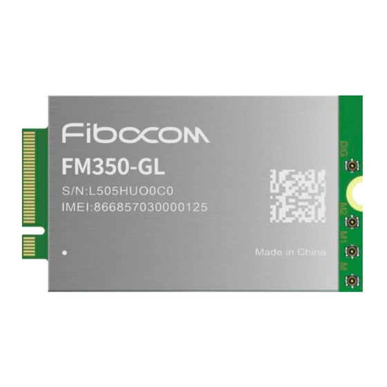
The product appearance for FM350 module is shown in Figure 6-1: Figure 6-1 Module appearance 6.2 Dimension of Structure The structural dimension of the FM350 module is shown in Figure 6-2: Reproduction forbidden without Fibocom Wireless Inc. written authorization - All Rights Reserved. FM350-GL Hardware Guide Page 47 of 59... -
Page 48: Interface Model
(30x52mm, the component maximum height on t top layer is 1.5mm, PCB thickness is 0.8mm, and KEY ID is B). Reproduction forbidden without Fibocom Wireless Inc. written authorization - All Rights Reserved. FM350-GL Hardware Guide Page 48 of 59... -
Page 49: Connector
APCI0026-P001A manufactured by LOTES Corporation, and the dimensions is shown in Figure 6-4. The package of connector, please refer to the specification. Figure 6-4 M.2 Dimension of structure Reproduction forbidden without Fibocom Wireless Inc. written authorization - All Rights Reserved. FM350-GL Hardware Guide Page 49 of 59... -
Page 50: Storage
The FM350 module uses tray package, 20 pcs are packed in each tray, with 5 trays including one empty tray on top in each box and 5 boxes in each case. Tray packaging process is shown in Figure 6-5: Reproduction forbidden without Fibocom Wireless Inc. written authorization - All Rights Reserved. FM350-GL Hardware Guide... - Page 51 Figure 6-5 Tray packaging process Reproduction forbidden without Fibocom Wireless Inc. written authorization - All Rights Reserved. FM350-GL Hardware Guide Page 51 of 59...
-
Page 52: Tray Size
Tray size The pallet size is 330x170x6.5mm, and is shown in Figure 6-6: Figure 6-6 Tray size (Unit: mm) Reproduction forbidden without Fibocom Wireless Inc. written authorization - All Rights Reserved. FM350-GL Hardware Guide Page 52 of 59... -
Page 53: Ce Conformance Information
7 CE Conformance information The device could be used with a separation distance of 20cm to the human body. Hereby, [Fibocom Wireless Inc.] declares that the radio equipment type [FM350-GL] is in compliance with Directive 2014/53/EU. 8 FCC Conformance information Important Notice to OEM integrators 1. - Page 54 5G NR n41 LTE B25 5G NR n66 LTE B26 5G NR n71 LTE B30 5G NR n77 LTE B38 5G NR n78 Reproduction forbidden without Fibocom Wireless Inc. written authorization - All Rights Reserved. FM350-GL Hardware Guide Page 54 of 59...
- Page 55 This equipment has been tested and found to comply with the limits for a Class B digital device, pursuant Reproduction forbidden without Fibocom Wireless Inc. written authorization - All Rights Reserved. FM350-GL Hardware Guide...
- Page 56 As long as 2 conditions above are met, further transmitter test will not be required. However, the OEM integrator is still responsible for testing their end-product for any additional compliance requirements required with this module installed. Reproduction forbidden without Fibocom Wireless Inc. written authorization - All Rights Reserved. FM350-GL Hardware Guide Page 56 of 59...
- Page 57 Cet équipement doit être installé et utilisé avec un minimum de 20 cm de distance entre la source de rayonnement et votre corps. Reproduction forbidden without Fibocom Wireless Inc. written authorization - All Rights Reserved. FM350-GL Hardware Guide...
- Page 58 This transmitter module is authorized only for use in device where the antenna may be installed such that 20 cm may be maintained between the antenna and users. The final end product must be Reproduction forbidden without Fibocom Wireless Inc. written authorization - All Rights Reserved. FM350-GL Hardware Guide...
- Page 59 Le manuel de l'utilisateur final doit inclure toutes les informations réglementaires requises et avertissements comme indiqué dans ce manuel. Reproduction forbidden without Fibocom Wireless Inc. written authorization - All Rights Reserved. FM350-GL Hardware Guide Page 59 of 59...
Need help?
Do you have a question about the FM350-GL and is the answer not in the manual?
Questions and answers