
Related Manuals for BenQ DLP PROJECTOR PE8700


Summary of Contents for BenQ DLP PROJECTOR PE8700
-
Page 1: Service Manual
DLP PROJECTOR SERVICE MANUAL MODEL:PE8700 CAUTION BEFORE SERVICING THE PROJECTOR, READ THE SAFETY PRECAUTIONS IN THIS MANUAL. -
Page 2: Table Of Contents
1. Safety Precautions 2. Servicing Precautions 3. Engineering Specification 4. Spare Parts List 5. Block Diagram 6. Packing Description 7. Appearance Description 8. Alignment Procedure 9. Trouble Shooting Guide 10. Factory OSD Operation 11. Firmware upgrade procedure 12. RS232 Codes 13. -
Page 3: Safety Precautions
1. Be sure to read this manual before servicing and save it for future reference. 2. The lamp becomes extremely hot during operation. Allow the projector to cool for approximately 45 minutes prior to removing the lamp assembly for replacement. Do not operate lamps beyond the rated lamp life. -
Page 4: Engineering Specification
Superscripts indicate the method in Appendix B used for a given measurement, unless otherwise noted. 1.0 Image Quality 1.1 Brightness 1.1.1 Typical 1.1.2 Minimum 1.2 Brightness Uniformity 1.2.1 Typical 1.2.2 Minimum 1.3 Contrast Ratio 1.3.1 Peak Contrast 1.4 Light Leakage 1.4.1 Blue Edge 1.4.2 Light Leakage out of Active Area... - Page 5 1.9 Descriptive Image Quality 1.10 Lateral Color 1.11 Screen Size for Testing 2.0 Optical 2.1 Optical Structure 2.2 Projection Lens 2.2.2 F/# 2.2.3 Throw Ratio 2.2.4 Zoom Ratio 2.2.5 Focus and flare 2.3 Lamp 2.3.1 Maker 2.3.2 Model 2.3.3 Type 2.3.4 Lamp Wattage 2.3.5 Lamp life 2.4 Focus Distance...
- Page 6 2.7.1 PC Mode 2.7.2 Video Mode 3.0 Mechanical & Cosmetic 3.1 Dimensions 3.2 Weight 3.3 Security Slot 3.4 Feet 3.5 Lamp Replace Position 4.0 Compatibility 4.1 RGB 4.2 Video Signal 4.3 HDTV 4.4 Image Inversion 4.5 Scaling 4.6 Aspect ratio 5.0 Interface Connectors 5.1 RGB Input 5.2 Video Input...
- Page 7 6.2 Control 6.2.1 IR Receivers 6.2.1.1 Location 6.2.1.2 Range 7.0 Power Requirements 7.1 Power Supply 7.2 Power Consumption 7.3 Power Connector 8.0 Audible Noise Level 9.0 Thermal 9.1 Surface Metal 9.2 Surface Plastic 9.3 Exhaust Air 9.4 Screws, Terminals 10.0 Contamination 10.1 Prevention 10.2 Dust in Optical Path 11.0 Included Accessories...
- Page 8 14.4.1 Straight Drop 14.4.2 Tilt Over 14.5 Gas 14.6 Electrostatic Discharge 15.0 Regulatory 15.1 Safety Requirements 15.1 EMI Requirements 16.0 Packaging 16.1 Packaging Form 16.1.1 Dimensions 16.1.2 Weight 16.1.3 Palletization 16.1.4 Carton Labeling 16.2 Vibration 16.3 Drop Test 50mm Should be able to fall over from tilting without taking any damage.
- Page 9 Appendix A This part of the Optical Test Instruction describes those measurements to be executed during the production of the optical engines. Content: A1 BRIGHTNESS A2 BRIGHTNESS UNIFORMITY A3 BRIGHTNESS DIFFERENCE A4 ANSI CONTRAST A5 PEAK CONTRAST A6 LIGHT LEAKAGE A7 IMAGE DISTORTION A8 THROW RATIO A9 ZOOM RATIO...
- Page 10 Practical consideration 1. When measuring contrast manually, operators should not wear white clothing since light reflected from white clothing can influence the measurement. 2. Unless otherwise specified the projection lens is set in the widest zoom position since zoom function can influence the measurement. 3.
- Page 11 A2. BRIGHTNESS UNIFORMITY Unit: Brightness: Default Contrast: Default Uniformity = A3. BRIGHTNESS DIFFERENCE Unit: Brightness: Default Contrast: Default Brightness Difference= − A4. ANSI CONTRAST Unit: Contrast : 1 Brightness: Default Contrast: Default Contrast Ratio shall be determined from illuminance values obtained from a black-and-white ”chessboard”...
- Page 12 A5. PEAK CONTRAST Unit: Contrast : 1 Brightness: Default Contrast: Default Contrast Ratio = Lux value at the center of a solid white screen/the lux value of a solid black screen A6. LIGHT LEAKAGE Unit: Brightness: Default Contrast: Default Leakage = The maximum light leakage of a solid black screen outside the projected image A7.
- Page 13 A9. ZOOM RATIO Unit: Ratio : 1 Brightness: Default Contrast: Default Zoom ratio = maximum / minimum image diagonal size at a fixed projection distance. A10. FOCUS RANGE Unit: m (Max~Min) Brightness: Default Contrast: Default The minimum/maximum focus distance is the minimum/maximum projection distance (front side projection lens and the image lane), expressed in meter, at which the image is still at its best for focus.
- Page 14 Appendix B Design Verification Test Procedure 1.Purpose This standard establishes the environmental specification for projector related products, which defines the level of product performance and reliability in the field. It is not necessary the intent of these specification to simulate a typical user environment, but rather to provide for a level of product robustness that when applied over a wide range of manufacturing variability and environmental usage conditions.
- Page 15 3.Definition 3.1 Failure Criteria: The product is expected to perform to its full potential without loss of function, performance, critical parametric changes, and other undesirable anomalies, over the applied boundaries of this specification. The following product failure are not allowed within the boundaries defined in this specification: 1.Failure including permanent damage, critical parametic changes (optical performance defined in Appendix A), and latent defects.
- Page 16 Appendix C Drawings and Attachments Drawing 1: Top view of BENQ PE8700 video projector...
- Page 18 Appendix D HD2 Front Projection Image Quality Specification 1. SCOPE This document specifies the image quality requirements applicable to the HD2 Component Set for Front Projection image display. The HD2 Component Set provides digital imaging functionality based on Digital Micromirror Device (DMD) technology. 2.
- Page 19 2.8 Gray 6 test screen This screen is used to test light blemishes and bright pixels. All areas of the screen are colored at a specific gray level, based on MS Paint 0-255 RGB scale: 2.9 Gray 10 test screen This screen is used to test light blemishes and bright pixels.
- Page 20 2.12 Red Ramp test screen This screen is used to test light border blemishes and bright pixels. All areas of the active area are colored at a specific gray level, based on MS Paint 0-255 RGB scale: 3. ACCEPTANCE REQUIREMENTS 3.1 Test Conditions (as tested in OEM projector) ·...
- Page 21 Light Pixel Minor Blemishes Unstable Pixel Notes: 1. The acceptance basis for all cosmetic DMD defects will be the projected image tests referenced in Table 1. 2. Projected blemish numbers include the shadow of the artifact in addititon to the artifact itself.(Count=4) 4.
- Page 22 Appendix E Supporting Timings Table 1: Support Timings by DVI-I Input (Analog or Digital PC signals) Resolution 640 x 400 640 x 480 640 x 480 SVGA 800 x 600 SVGA 800 x 600 SVGA 800 x 600 1024 x 768 1024 x 768 1024 x 768 Table 2: Support Timing by DVI-I Input...
- Page 23 Table 3: EDTV and HDTV Timing supported by component (YPBPR) and RGBHV Input Index Format Line Pixel name Rate Rate (kHz) (MHz) 480i 15.734 13.5 576i 15.625 13.5 480p 31.469 27 576p 31.25 720p50 37.5 74.25 720p59 44.955 74.176 59.94 720p60 45 74.25 1080i25 28.125 74.25...
-
Page 24: Spare Parts List
PCBA TRANSLATION/BD HT720G ASSY CVR BASE HT720W/BENQ ASSY L/C HT720W/BENQ ASSY CVR FRONT HT720W/BENQ ASSY CVR BACK CONTOR HT720W ASSY CVR LENS HT720W BENQ PCBA THERMAL SENSOR/B HT480W PCB FPC/BD FOR HT480W PCBA CONNECTOR/BD FOR BENQ PCBA POWER BD HT480W MI... -
Page 25: Block Diagram
Conntctor Board RGB DVI RGB PC (U2,U3,U4) RGB/YPbPr YCbCr YPbPr (U5) S-video Video YCbCr IR Board RS232 RS232 RJ11 Download (U14) IR (TOP) (U12) 12V Trigger O/P (Q2,Q3) IR (front) IR Board Board 5. Black Diagram Main Board Sil169 (U17) ADC AD9883 (U7) De-interlace... -
Page 26: Packing Description
6. Packaging Description... -
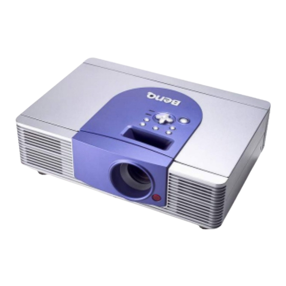
Page 27: Appearance Description
7. Appearance Description... -
Page 29: Alignment Procedure
1. DMD Bias Voltage Alignment Equipment: None Procedure: 1. Watch DMD chip Label 2. Switch the DIP switch on DMD board according to the character on the DMD chip 1 of SW H1 1 2 of SW H2 1 0: Left; 1:Right 2.Color Wheel Delay Alignment Equipment: Battery Biased Silicon PIN Detector... - Page 30 Procedure: 1. Probe impedance matches 50 ohm 2. Change Timing and pattern of pattern generator : Timing : 800x600@60Hz (H:37.879Khz,V:60.317Hz) pattern : full white 3. Adjust user & factory OSD values to default. 4. Open Factory OSD, and select color wheel delay item. 5.
- Page 31 3. DVI-Analog Color Alignment Procedure Default valve(User menu) contrast Video S-Video Comp Comp-HD RGBHV DVI-I The Gamma(RED ,GREEN,BLUE) is Equipment: Pattern generator (Chroma 2250) Lux meter ( CL-100) OSD Default value used for DVI-Analog color alignment Item USER>Picture> Brightness Contrast Color Tint Sharpness...
- Page 32 Procedure: A. Black Level Adjustment: (DLP brightness) Change pattern of pattern generator : Pattern : Black (Gray 0) Adjust DLP Brightness to let the black picture to just distinguish. B. White Level Adjustment: (AD contrast---R,G,B gain) 1. Change pattern of pattern generator : pattern : White (100% Gray) 2.
- Page 33 3 The variance of color coordinate via R,G,B gains: R ↓ G ↓ B ↓ 4. Adjust 6500K temperature color by changing Gamma-Rgain, Ggain, and Bgain. 5. Open Factory OSD and set the factory default value : user>setup>white Gamma-Rgain Gamma-Ggain Gamma-Bgain User the lux meter and adjust Gamma-Rgain, Gamma-Ggain, &...
- Page 34 Filter Color Temp Procedure: (a). PBPR Offset adjustment: (AD PB, PR Offset) 1. The variance of color coordinate via Pb offset and Pr offset: Pb offset ↓ Pb offset ↑ Pr offset ↓ Pr offset ↑ If we line the x and y, then the Pb offset is the shift action and the Pr offset is the rotational action.
- Page 35 (c). Saturation Level: (Scalar) 1. Change Timing and pattern of pattern generator : Timing : 480P(H:31.54 KHz,V:60.08 Hz) pattern : 100% blue 2. Adjust saturation and use lux meter to measure to let the light output just max. Select “Save Setting” at “Factory OSD>Factory>”. Case x1>x0 &...
- Page 36 Case x1>x0 & y1 > y0 : y =.331 x =.291 x =.281 dec. Pb x0 =.281 y0 =.311 x0 =.281 x =.301 y =.321 x =.291 dec. Pb x0 =.281 y0 =.311 x0 =.281 Case x1<x0 & y1 < y0 : inc.
- Page 37 5. TV Color Alignment Procedure 5.1 TV Color Temp Alignment Equipment: Pattern generator (VG-828) Lux meter ( CL-100) OSD Default value used for YCBCR color temp alignment Item USER>Picture> Brightness Contrast Color Tint Sharpness Filter Color Temp 1. Connect the signal to YCBCR component connector, and change Timing and pattern of pattern generator : Timing : NTSC(H:15.73 KHz,V:29.96 Hz) pattern : 80% Gray...
- Page 38 6. User the lux meter and adjust Gamma-Rgain, Gamma-Ggain, & Gamma-Bgain to meet the spec. 7. Press “Save Color Temp. Videos > AS Color Temp 5400” to save into memory. 8. Repeat 6~7 to perform the 6500K and 7500K color temperature. 9.
- Page 39 5.3 Gray Level for Composite Video & S-Video Equipment: Pattern generator (VG-828) Lux meter ( CL-100) OSD Default value: Item USER>Picture> Brightness Contrast Color Tint Sharpness Filter Color Temp Procedure: (a) Gray Level 1. Connect power, Composite video or S-Video, into projector. 2.
-
Page 40: Trouble Shooting Guide
1. System trouble shooting : Is LED light when Main Power Switch Is Orange LED active when remote power on? Is lamp turned on? Does starting OSD shows normally? Does DVI-I signal shows normally? Does Video signal shows normally? 9. Trouble Shooting Guide Check door luck switch Are fans spinning? - Page 41 2. Main board trouble shooting: (1) Main: REMOTE POWERON OSD ok? When no valid signal OSD ok. When input PC signal OSD ok. When input Video signal Saving data in EEPROM 1. See CPU trouble shooting U18, reset successful? 2. U17, RP25, RP24 OK? CPU (U10) 56pin(IR) signal? 1.
- Page 42 (2) SIL504 trouble shooting: (U4, U2) X1, 20Mhz? RESET successful? System IIC ok? (U4 pin 15,14) SIL504 IIC ok? (U4 pin 2, 3) DEINTDONE Signal ok? (U4 pin21) 1. check X1, C41, C42 check U17,RP25 1.Q2,Q3 ok? (level shift ) 2.
- Page 43 (3) CPU (U10) trouble shooting guide : Check +3Vs (pin92) Check X1 crystal RESET Successful? 1. Check U9(SRAM), check CPU_LCS_N (pin 58) and CPU_BHE_N is active? 2. Check U12(Flash), check R68 and CPU_UCS_N (pin 57) is active? 1. Check C75, C76 2.
- Page 44 3. DMD board trouble shooting guide. RESETZ And POWERGOO Color wheel Spinning? Color wheel Feedback (J3 pin3) ok? Lamp light ok? Normal Image DMD pixels always on on screen ? (32-Gray Pattern in Factory mode Horizontal dark/bright lines recommended) Vertical dark/bright lines Color missing 1.
- Page 45 4. Connector board trouble shooting guide. S-video is OK? Composite is Component is DVI- A is DVI-D (HDCP)is YPbPr is OK? BNC-PC is OK? J6 12V output? Check L14,L17 Check U5 Check U10 Check L13 Check U5 Check U10 Check L15,L16,L18 Check U10 Check L28,,L29,L31,L32,L33 Check U17...
- Page 46 RS232 is OK? 5. Power board trouble shooting guide. P o w e r B D C h e c k . F u s e B r o k e n ? Y e s P r o c e e d to " P r im a r y C ir c u it C h e c k "...
- Page 47 + 1 2 V O u t p u t C h e c k 1 2 V e x i s t s Y e s C h e c k Q 7 0 3 w o r k s n o r m a l l y ? ( V c e <...
- Page 48 N o 1 2 V o u t p u t N o + 5 V - F i x o u t p u t C h e c k D 7 0 1 h a d b e e n i n s e r t e d p r o p e r l y ? Y e s C h e c k I C 7 0 1 d a m a g e s ?
- Page 49 C h e c k p rim a r y c ir c u it. F u s e B r o k e n ? Y e s C h e c k Q 6 0 1 d a m a g e s ? Y e s P in D &...
-
Page 50: Factory Osd Operation
There are 10 pages in this OSD, the ways to enter factory OSD are open user OSD, then press power on button. If you have to return user OSD, open factory OSD and press power on button again. Go to \User OSD\Environment\lamp hours\minutes, then press Right, Left, Right, Left, Enter in a row to switch to factory OSD. - Page 51 2. HD Adj This page is the settings of A/D converter. There are 2 sections, one is for RGBHV format signal (DVI-A input and RGB-HD input), the other is for YPbPr format signal (Comp-HD input). Page RGBHV format Page YPbPr format 3.
- Page 52 Page Component 4. Color Balance For color temperature settings, they are the combination of gamma gain and gamma offset. This page allows operator to adjust gamma correction to fit the expected color temperature, and save these settings as one of the color temperature settings. And this page also provides the function to restore color temperature setting to default gamma combination.
- Page 53 Page Save gamma gain and gamm offset as color temp 9300K Save gamma gain and gamm offset as color temp 6500K Save Data Temp. Save gamma gain and gamm offset as color temp 5700K Restore combination Page Save gamma gain and gamm offset as color temp 9300K Save gamma gain and gamm offset as color temp 6500K...
- Page 54 6. DLP This page allows user to change DLP settings. Page 7.Pattern1 This page allows user to call up DLP present curtains and RM-1A patterns. Page Red Curtain Green Curtain Blue Curtain Black Curtain Patterns 1 Color Bar Checker Board 13-Points Reflective Edge Items...
- Page 55 8.Pattern2 This page allows user to call up DLP DDP1010 series present patterns. Page Solid Field - Yellow Solid Field - Cyan Solid Field - Magenta DLP DDP1010 present pattern. For checking color. Horizontal Ramp Patterns 2 Vertical Ramp Horizontal Lines Diagonal Lines Vertical Lines Grid...
- Page 56 White Full Black Full Red Ramp 10 . Test Mode For different situation, we need different settings. Here we define 5 kinds of settings in ‘Picture Adjust’ page to fit some situations. Page Optical Test Middle Value Test Mode Play DVD Color Wheel Delay Blue Filter DLP DDP1010 present pattern.
-
Page 57: Firmware Upgrade Procedure
11. Firmware Upgrade Procedure Connect specific download cable to RS232 (RJ-11) connector. Remember to turn the AC switch off. Execute the ‘Flash Loader’ program. If the ‘COM Settings’ item is ready, you can see ‘Identifying target…’ at the bottom of flash loader. If not, open ‘COM Settings’ item. Choose the ‘COM Port’... - Page 58 Turn the AC switch on. In 3 seconds, ‘flash loader’ will identify the flash ROM of this unit. Choose ‘Hex File Format’ as ‘Intel Extended’, ‘Operation’ as ‘Program’, and ‘Browse’ the ‘File Name’. After that, press the ‘Start’ button. ‘Flash Loader’ starts to load program to Flash ROM.
-
Page 59: Rs232 Codes
1. Set up peripherals BenQ PE8700 provides an RJ-11 connector for RS232 serial communication control. The user can use the ‘Hyper Terminal’ program of Microsoft Windows to control this unit. To set the settings of serial port first is necessary. Choose which COM port you want... - Page 60 After settling down, connect our specific RS232 cable and press the ‘call’ icon of ‘Hyper Terminal’ program. After this, press ‘Enter’ key, if an ‘>’ symbol come up, that means the unit is ready to accept commands for computer. 2. Commands list There are 3 kinds of serial commands, X-group, Y-group and Z-group.
- Page 61 Code Must be Reversed , no function Power On Power Off Message On Message Off Lamp hours reset Load all user OSD default value Save current active source settings Change active OSD Menu Enter Exit Up(arrow key) Down(arrow key) Left(arrow key) Right(arrow key) Switch to Composite input Switch to S-Video input...
- Page 62 Aspect - Standard (4:3) Aspect - Letter box Aspect - Virtual wide Aspect - Through Load memory 1 settings Load memory 2 settings Load memory 3 settings Load 'optical test' mode settings Load 'middle' mode settings Load 'CW delay adjustment' mode settings Load default of current source Save memory 1 settings Save memory 2 settings...
- Page 63 Image orientation - floor front Image orientation - ceiling front Image orientation - floor rear Image orientation - ceiling rear Back light board On Back light Board Off On line help When an user sends a command, he must follow the command format in the list. After he sends a command, program will acknowledge 2 pieces of information.
- Page 64 Following is the list of Y-group: Code Save current factory settings Load saved factory settings Load factory default Load all user default Burn-In mode on Burn-In mode off Set RS232 baudrate as 9600 Set RS232 baudrate as 115200 Save as data color temperature 1 Save as data color temperature 2 Save as data color temperature 3 Save as video color temperature 1...
- Page 65 Red Curtain Green Curtain Blue Curtain Black Curtain Color Bar Chess Board Optical 13-point Reflective Edge Grid Blue 90 Curtain Gray 10 Curtain Gray 6 Curtain Full White Curtain Full Black Curtain Red Ramp Curtain Gray 20 Curtain Load 'optical test' mode settings Load 'middle value' mode settings Load 'Play DVD' mode settings Load 'CW delay adjustment' mode settings...
- Page 66 Example: 1. Command = Y89893 (Enter) ACK = Y1Y (Illegal format, wrong length) 2. Command = Y98 (Enter) ACK = Y2Y (Illegal function) 3. Command = Y52 (Enter) ACK = Y0Y ACK = Y0_52Y For Z-group, this one is for ‘auto-alignment’ procedure in our factory. This one allows engineers to read or write the unit settings without OSD operation, it will save time to set the value.
- Page 67 Z030 Keystone adjustment Z034 RGBHV input -- Red offset Z035 RGBHV input -- Green offset Z036 RGBHV input -- Blue offset Z037 RGBHV input -- Red gain Z038 RGBHV input -- Green gain Z039 RGBHV input -- Blue gain Z042 YPbPr input -- Brightness Z043 YPbPr input -- Contrast...
- Page 68 Z069 Z070 Z071 Z072 Z073 Z080 Z099 The length of the command must be 11. The format, take an example, to read DMD color wheel delay: Z072RxxxxxZ, where Byte 1: must be 'Z' or 'z' Byte 2~4: function code Byte 5: action, must be ‘r’ or ‘R’ Byte 6~10: Don’t care Byte 11: must be 'Z' or 'z' In contrast, if write DMD color wheel delay:...
- Page 69 And the length of ACK must be 12, and format is Z0_072+0025Z Byte 1: Always ‘Z’ Byte 2: ACK Byte 3: Always ‘_’ Byte 4~6: function code Byte 7: sign byte, ‘+’ or ‘-‘ Byte 8~11: the current value after writing Byte 12: Always ‘Z’...
-
Page 70: Schematics
POWER DMD_SCL DMD_SDA +12VA +5VS +3VS +5VA +3VA +12VA +5VA +5VS +3VA +3VS Benq Corporation Project Code Model Name OEM/ODM Model Name HT720G 99.J5877.001 Title MAIN BOARD Size PCB P/N P CB Rev. Document Number R e v . <Size>... - Page 71 KEYPAD[0..9] KEYPAD9 +3VS 74HC132 BACK_LIGHT_CTRL FAN_CTRL DLP_RST POWERON DLP_RESETZ LAMP_PROTECT +3VS CON_12P +3VS THERMAL CONNECTOR Benq Corporation Project Code Model Name HT720G 99.J5877.001 Title MAIN BOARD Size PCB Rev. PCB P/N <Size> 48.J5801.S02 Thursday, January 16, 2003 Date: Prepared By...
- Page 72 HOLE-V8 +5VS Optical Points OP10 OP11 OP15 OP16 OP17 OP18 HOLE-V8 OP12 OP13 OP14 Benq Corporation Project Code Model Name OEM/ODM Model Name HT720G 99.J5877.001 Title MAIN BOARD Size PCB P/N P CB Rev. Document Number R e v .
- Page 73 V_IN12 DI_I N6 V_IN13 DI_I N7 NC_RP V_IN14 DI_I N8 V_IN15 DI_I N9 VCLK NC_R0603 DI_27M_CLK Benq Corporation Project Code Model Name OEM/ODM Model Name HT720G 99.J5877.001 Title MAIN BOARD Size PCB P/N P CB Rev. Document Number R e v .
- Page 74 PRMODE1 ENABLE GPIO0 FILMBIAS GPIO1 SUBTITLE GMODE EXTGMD MCKSEL SQMODE YPRPB RSVD0 WAVE OSC1 OSC2 MCU503 Benq Corporation Project Code 99.J5877.001 Title Size PCB P/N <Size> Thursday, January 16, 2003 Date: Prepared By ANGEL HU +5VA LED_1206 LED_1206 DI_SDA DI_SCL...
- Page 75 MEM_DQ35 MEM_DQ37 VDD33 MEM_DQ34 MEM_DQ31 MEM_DQ33 MEM_DQ32 MEM_DQ30 MEM_DQ28 MEM_DQ29 MEM_DQ27 MEM_DQ26 MEM_DQ25 Benq Corporation Project Code Model Name OEM/ODM Model Name HT720G 99.J5877.001 Title MAIN BOARD Size PCB P/N P CB Rev. Document Number R e v . <Size>...
- Page 76 RM1_IRQ RM1CLKIN CPU _WR_N CPU_R D_N CPU_MCS1_N CPU_MCS2_N CPU_MCS3_N +3VS +3VS +3VA +5VA +12VA Benq Corporation Project Code Model Name OEM/ODM Model Name HT720G 99.J5877.001 Title MAIN BOARD Size PCB P/N P CB Rev. Document Number R e v .
- Page 77 R118 100K BAV99 1U Z ** Generate Harward RESET Singnal ** SOT23 +3VS 0.1UF 0.1UF 0.1UF 0.1UF 0.1UF Benq Corporation Project Code Model Name OEM/ODM Model Name HT720G 99.J5877.001 Title MAIN BOARD Size PCB P/N P CB Rev. Document Number R e v .
- Page 78 DLP_RESETZ POWERON DLPSP R124 DLP_SPARE +3VA R125 0 SYNCVALID BALLAST_CTRL R126 +5VA OP_FIELD THIS PIN ONLY FOR TEST Benq Corporation Project Code Model Name 99.J5877.001 Title MAIN BOARD Size PCB P/N <Size> 48.J5801.S02 Thursday, January 16, 2003 Date: Prepared By...
- Page 79 MEM_A5 MEM_A6 MEM_A7 MEM_A8 MEM_A9 MEM_A10 MEM_A11 MEM_BS MEM_CS_N MEM_WE_N MEM_RAS_N MEM_CAS_N MEM_CLK Benq Corporation Project Code Model Name OEM/ODM Model Name HT720G 99.J5877.001 Title MAIN BOARD Size PCB P/N P CB Rev. Document Number R e v . <Size>...
- Page 80 120 OHM 0.047U K 0.047U K 4.7U Z (1206) 510K 2V_REF 6.8K LMC7225 CWSPPED1 CWINDEX CIRCUIT INPUTS, LAMPEN, LAMPLIZ, CWINDEX Benq Corporation Project Code 99.J5877.001 Title Size PCB P/N <Size> 48.J5802.S01 Tuesday, January 14, 2003 Date: Prepared By ANGEL HU...
- Page 81 TP47 TP48 TSTPNT3 TSTPNT2 TSTPNT1 TSTPNT0 (v-sync, delay CWI, spoketest for debug) TP36 50MHz Clock DDP1010 Flash, Micro, Clocks, DAD1000 Control OCLKA1 OCLKA Benq Corporation PUM_ARSTZ Project Code (To DAD1000) EXT_ARSTZ 99.J5877.001 Title Size PCB P/N TP34 TP35 <Size> Tuesday, January 14, 2003...
- Page 82 AG14 SCTRLBP SCBP AH14 SCTRLBN SCBN AA27 RMHSOZ AA28 RMVSOZ DDP1010 Video Input and DMD Output HSYNCOZ VSYNCOZ Benq Corporation Project Code AA29 FSD16 99.J5877.001 Title Size PCB P/N <Size> 48.J5802.S01 Tuesday, January 14, 2003 Date: Prepared By ANGEL HU DDAP[15..0]...
- Page 83 120 OHM C184 C185 C186 C187 C188 0.1U Z 4.7U Z 0.1U Z 68P J 0.1U Z (1206) C229 Benq Corporation 150U 6.3V Project Code 99.J5877.001 Title Size PCB P/N <Size> 48.J5802.S01 Tuesday, January 14, 2003 Date: Prepared By ANGEL HU VTERM 1.8V...
- Page 84 RD_RSGND13 RD_RSGND12 RD_RSGND11 RD_RSGND10 RD_RSGND9 RD_RSGND8 RD_RSGND7 RD_RSGND6 RD_RSGND5 RD_RSGND3 RD_RSGND2 RD_RSGND1 DDP1010 Benq Corporation Project Code Model Name OEM/ODM Model Name HT720G 99.J5877.001 Title DMD BOARD Size P CB Rev. Document Number R e v . PCB P/N <Size>...
- Page 85 0.1U 0.1U 0.1U 0.1U P3P3V 120 OHM C111 C112 0.1U Z 0.1U Z TP10 MBRST[15..0] TP11 TP12 Benq Corporation Project Code 99.J5877.001 Title Size PCB P/N <Size> 48.J5802.S01 Tuesday, January 14, 2003 Date: Prepared By ANGEL HU VCC2 C113 C114...
- Page 86 0.1U Z (50V) --> (1U--> 0.22U) for more working margin 0.22U M (0805) VRST 4.7U Z 0.1U Z 0.1U Z (50V) 22UH Benq Corporation Project Code 99.J5877.001 Title Size PCB P/N <Size> Tuesday, January 14, 2003 Date: Prepared By ANGEL HU...
- Page 87 FDS6930A NC_R1206 NC_R0805 NC_R0805 NC_0805 (1206) (0805) (0805) (0805) (0805) (0805) (0805) SSI COLOR WHEEL DRIVE CIRCUIT Benq Corporation Project Code 99.J5877.001 Title Size PCB P/N <Size> Tuesday, January 14, 2003 Date: Prepared By ANGEL HU V12A 15V,1.5W,5% 0.1U Z...
- Page 88 0.1U Z OUT_R OUT_RED OUT_G OUT_GREEN OUT_BLUE OUT_B 2022012015 +V_DAC BAV99 BAV99 VSYNC_OUT HSYNC_OUT Optical Points Benq Corporation Project Code HOLE-V8 99.J5877.001 Title Size PCB P/N <Size> 48.J5824.S02 Wednesday, January 15, 2003 Date: Prepared By ANGEL HU +V_DAC 0.047U K...
- Page 89 DLP_RESETZ Ballast_Ctrl POWERON PWRGOOD SYNCVALID +12VA +5VA 20C1001100 POWER +12VA 12VA 500 OHM (1206) 0.1U K Benq Corporation Project Code 99.J5877.001 Title Size PCB P/N <Size> 48.J5824.S02 Wednesday, January 15, 2003 Date: Prepared By ANGEL HU LAMPLITZ (For HD2) (For HD2)
- Page 90 6_Trigger/3D/Thermal/RS232 DVI_ACTDATA DI_IN[2..9] DI_27M_CLK DI_VSYNC DI_HSYNC RESET_DEC CPU_TXD0 CPU_RXD0 +5V_AD +12VA MUX_SEL +3VD +5VS MUX_SEL_P Benq Corporation +3VD MUX_BUFFER +5VS Project Code +5V_AD 99.J5877.001 Title +12VA Size PCB P/N 7_120Pin B2B Connector <Size> Monday, February 17, 2003 Date: Prepared By...
- Page 91 V SYNC MUXPP R73 0 MUX_SEL_Q +5V_MUX 74126(73.74126.0HB) 1:BNC-HV 5.1K SEL_HV 0:DSUB-HV 2N3904 2N3904 Benq Corporation Project Code Model Name OEM/ODM Model Name HT720G 99.J5877.001 Title CONNECTOR BOARD Size P CB Rev. Document Number R e v . PCB P/N <Size>...
- Page 92 0.1UF RCA 3 IN 1 (open) (open) Y C C FCB3216K C153 C154 0.1UF 0.1UF (open) (open) +5V_AV +5V_AD Benq Corporation 0.1UF 0.1UF 0.1UF 0.1UF Project Code 99.J5877.001 For AD8183 Title Size PCB P/N <Size> Monday, February 17, 2003 Date:...
- Page 93 C182 C183 C184 C185 C186 0.1U Z 0.1U Z 0.1U Z 0.1U Z 0.1U Z 0.1U Z Benq Corporation Project Code Model Name OEM/ODM Model Name HT720G 99.J5877.001 Title CONNECTOR BOARD Size P CB Rev. Document Number R e v .
- Page 94 0.1UF 0.1UF 0.1UF 0.1UF DI_VSYNC DI_HSYNC DI_27M_CLK TP49 TP50 TP51 TP52 TP53 DI_IN[2..9] Benq Corporation Project Code Model Name OEM/ODM Model Name HT720G 99.J5877.001 Title CONNECTOR BOARD Size P CB Rev. Document Number R e v . PCB P/N <Size>...
- Page 95 SCD437 C115 C116 10UF/25 0.1UF NC_R1206 NC_R1206 2213008001 RXX1 TXX1 C126 C127 47PF/50 47PF/50 Benq Corporation Project Code 99.J5877.001 Title Size PCB P/N <Size> Monday, February 17, 2003 Date: Prepared By ANGEL HU Model Name OEM/ODM Model Name HT720G CONNECTOR BOARD PCB Rev.
- Page 96 FCB3216K C133 0.1UF Optical Points OP10 OP11 OP12 +5VS +5VS C128 0.1UF HOLE-V8 HOLE-V8 HOLE-V8 HOLE-V8 +12VA Benq Corporation Project Code Title Size PCB P/N <Size> Date: Prepared By OP13 OP14 OP15 OP16 HOLE-V8 HOLE-V8 HOLE-V8 Model Name OEM/ODM Model Name HT720G 99.J5877.001...
- Page 97 AME8500BEETAF29 C176 1U Z +5V_EDID R107 R108 R109 4.7K 4.7K DVI_SCL DVI_SDA AT24C16 16K Benq Corporation Project Code Model Name OEM/ODM Model Name HT720G 99.J5877.001 Title CONNECTOR BOARD Size P CB Rev. Document Number R e v . PCB P/N <Size>...
Need help?
Do you have a question about the DLP PROJECTOR PE8700 and is the answer not in the manual?
Questions and answers