Table of Contents
Advertisement
Quick Links
See all versions
of this document
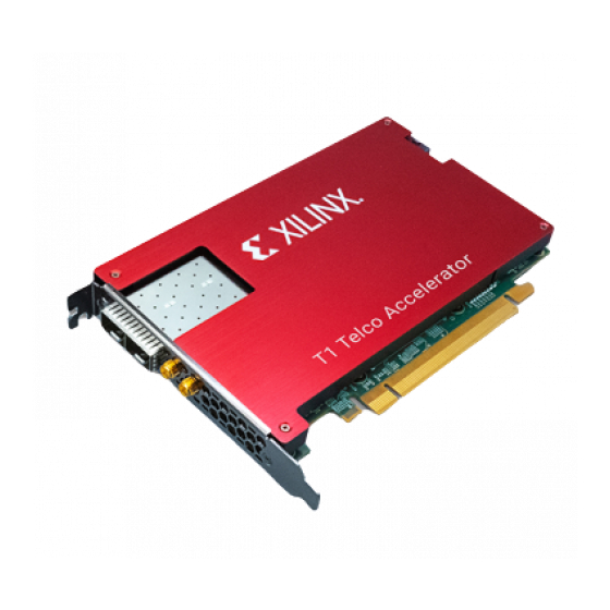
T1 Telco Accelerator Card
User Guide
UG1495 (v1.0) December 17, 2021
Xilinx is creating an environment where employees, customers, and
partners feel welcome and included. To that end, we're removing non-
inclusive language from our products and related collateral. We've
launched an internal initiative to remove language that could exclude
people or reinforce historical biases, including terms embedded in our
software and IPs. You may still find examples of non-inclusive
language in our older products as we work to make these changes and
align with evolving industry standards. Follow this
link
for more
information.
Advertisement
Table of Contents

Related Manuals for Xilinx T1


Summary of Contents for Xilinx T1
- Page 1 T1 Telco Accelerator Card User Guide UG1495 (v1.0) December 17, 2021 Xilinx is creating an environment where employees, customers, and partners feel welcome and included. To that end, we’re removing non- inclusive language from our products and related collateral. We’ve...
-
Page 2: Table Of Contents
MAC to MAC Interface Reference Clock..................36 User Clocks..........................36 Chapter 5: LEDs ......................38 Chapter 6: Xilinx Design Constraints (XDC) File .......... 39 Appendix A: Programming the Devices Using JTAG ........40 Flashing the Images to ZU19 Zynq UltraScale+ MPSoC QSPI Using SDK......43 Flashing the Images to ZU21 Zynq UltraScale+ RFSoC QSPI Using SDK...... - Page 3 Appendix C: Additional Resources and Legal Notices ......52 Xilinx Resources.........................52 Documentation Navigator and Design Hubs.................52 References..........................53 Revision History......................... 53 Please Read: Important Legal Notices................... 53 UG1495 (v1.0) December 17, 2021 www.xilinx.com Send Feedback T1 Telco Accelerator Card User Guide...
-
Page 4: Chapter 1: Introduction
16 nm Zynq ® UltraScale+™ MPSoC and Zynq UltraScale+ RFSoC devices. The T1 form factor is full height, half length (FHHL) and single slot, with a PCIe Gen 3 x16 interface that is x8x8 bifurcated providing x8 links from the host to each MPSoC and RFSoC device. Target applications for the T1 card include: •... -
Page 5: Features
Chapter 1: Introduction Features A high-level block diagram of the T1 card card is shown in the following figure. Figure 2: T1 card High-Level Block Diagram 4GB DDR4 2GB DDR4 4GB DDR4 2GB DDR4 (PL) (PS) (PL) (PS) SFP28 Optics... -
Page 6: Overview
SoCs. A second set of DDR4 memory is interfaced to PS section of both SoCs. One 100G transceiver is implemented on both SoCs for inter-SoC communication. A detailed block diagram of the T1 card card is shown in the following figure. Figure 3: Detailed T1 card Block Diagram... - Page 7 0.85V VCCINT core voltage. A comparison of the features of this device relative to other devices in the same family is shown in the following figure. Refer to the Zynq UltraScale+ RFSoC Product Selection Guide for further details. UG1495 (v1.0) December 17, 2021 www.xilinx.com Send Feedback T1 Telco Accelerator Card User Guide...
- Page 8 Chapter 1: Introduction Figure 5: Zynq UltraScale+ RFSoC XCZU21DR Device UG1495 (v1.0) December 17, 2021 www.xilinx.com Send Feedback T1 Telco Accelerator Card User Guide...
-
Page 9: Chapter 2: Pin Mapping
Clock: SFP0 & SFP1 Diff Clock2 Input (Neg) AT19 MP_156.25MHZ_CLK2_P Clock: SFP0 & SFP1 Diff Clock2 Input (Pos) AK22 AUX_GPIO GPIO - Zynq UltraScale+ MPSoC <-- >Clock Synth UG1495 (v1.0) December 17, 2021 www.xilinx.com Send Feedback T1 Telco Accelerator Card User Guide... - Page 10 GPIO - Zynq UltraScale+ MPSoC <-->SC AH19 SOC_SCL I2C Bus AJ18 SOC_SDA I2C Bus MAC_MP_T0_N Inter-SoC 100G MAC MAC_MP_T0_P Inter-SoC 100G MAC MAC_MP_T1_N Inter-SoC 100G MAC MAC_MP_T1_P Inter-SoC 100G MAC UG1495 (v1.0) December 17, 2021 www.xilinx.com Send Feedback T1 Telco Accelerator Card User Guide...
- Page 11 AM16 PCIE_MP_PERST_LS# PCIe AH17 PCIE_MP_WAKE_LS# PCIe PCIE_RX0_N PCIe PCIE_RX0_P PCIe PCIE_RX1_N PCIe PCIE_RX1_P PCIe PCIE_RX2_N PCIe PCIE_RX2_P PCIe PCIE_RX3_N PCIe PCIE_RX3_P PCIe PCIE_RX4_N PCIe PCIE_RX4_P PCIe UG1495 (v1.0) December 17, 2021 www.xilinx.com Send Feedback T1 Telco Accelerator Card User Guide...
- Page 12 PL 72-bit DDR4 PL_DDR4_2_BA0 PL 72-bit DDR4 PL_DDR4_2_A1 PL 72-bit DDR4 PL_DDR4_2_A2 PL 72-bit DDR4 PL_DDR4_2_TEN PL 72-bit DDR4 PL_DDR4_2_WE# PL 72-bit DDR4 PL_DDR4_2_A3 PL 72-bit DDR4 UG1495 (v1.0) December 17, 2021 www.xilinx.com Send Feedback T1 Telco Accelerator Card User Guide...
- Page 13 PL 72-bit DDR4 PL_DDR4_2_DQ20 PL 72-bit DDR4 PL_DDR4_2_DQ29 PL 72-bit DDR4 PL_DDR4_2_DQ27 PL 72-bit DDR4 PL_DDR4_2_DQ31 PL 72-bit DDR4 PL_DDR4_2_DQ26 PL 72-bit DDR4 PL_DDR4_2_DQ28 PL 72-bit DDR4 UG1495 (v1.0) December 17, 2021 www.xilinx.com Send Feedback T1 Telco Accelerator Card User Guide...
- Page 14 PL 72-bit DDR4 PL_DDR4_2_DQ59 PL 72-bit DDR4 PL_DDR4_2_DQ7 PL 72-bit DDR4 PL_DDR4_2_DQ61 PL 72-bit DDR4 PL_DDR4_2_DQ57 PL 72-bit DDR4 PL_DDR4_2_DQ56 PL 72-bit DDR4 PL_DDR4_2_DQ60 PL 72-bit DDR4 UG1495 (v1.0) December 17, 2021 www.xilinx.com Send Feedback T1 Telco Accelerator Card User Guide...
- Page 15 PL 72-bit DDR4 PL_DDR4_2_A12 PL 72-bit DDR4 PL_DDR4_2_ODT PL 72-bit DDR4 MP_DDR4_GATING PL 72-bit DDR4 (gating signal) PPS_IN_PL PPS Input MPSOC_PPS_OUT PPS Output BA30 PS_DDR4_2_A0 PS 36-bit DDR4 UG1495 (v1.0) December 17, 2021 www.xilinx.com Send Feedback T1 Telco Accelerator Card User Guide...
- Page 16 PS 36-bit DDR4 AY27 PS_DDR4_2_DQ28 PS 36-bit DDR4 BB25 PS_DDR4_2_DQ31 PS 36-bit DDR4 AU25 PS_DDR4_2_DQ1 PS 36-bit DDR4 AR25 PS_DDR4_2_DQ4 PS 36-bit DDR4 AT22 PS_DDR4_2_DQ6 PS 36-bit DDR4 UG1495 (v1.0) December 17, 2021 www.xilinx.com Send Feedback T1 Telco Accelerator Card User Guide...
- Page 17 PS 36-bit DDR4 AR24 PS_DDR4_2_DQS0_P PS 36-bit DDR4 AU27 PS_DDR4_2_DQS2_N PS 36-bit DDR4 AU26 PS_DDR4_2_DQS2_P PS 36-bit DDR4 BA38 PS_DDR4_2_DQS4_N PS 36-bit DDR4 BA37 PS_DDR4_2_DQS4_P PS 36-bit DDR4 UG1495 (v1.0) December 17, 2021 www.xilinx.com Send Feedback T1 Telco Accelerator Card User Guide...
- Page 18 AT17 SFP0_REC_CLK_C_N SFP0 AT18 SFP0_REC_CLK_C_P SFP0 SFP0_RX_LOS SFP0 SFP0_RX_N SFP0 SFP0_RX_P SFP0 SFP0_TX_DISABLE SFP0 SFP0_TX_FAULT SFP0 SFP0_TX_N SFP0 SFP0_TX_P SFP0 SFP1_161.13MHZ_CLK_N SFP1 SFP1_161.13MHZ_CLK_P SFP1 SFP1_IN_CLK_C_N SFP1 UG1495 (v1.0) December 17, 2021 www.xilinx.com Send Feedback T1 Telco Accelerator Card User Guide...
-
Page 19: Zynq Ultrascale+ Rfsoc Zu21 Pin Map
>Zynq UltraScale+ RFSoC PL GP10 GPIO - Zynq UltraScale+ MPSoC <-- >Zynq UltraScale+ RFSoC PL GP11 GPIO - Zynq UltraScale+ MPSoC <-- >Zynq UltraScale+ RFSoC PL UG1495 (v1.0) December 17, 2021 www.xilinx.com Send Feedback T1 Telco Accelerator Card User Guide... - Page 20 Inter-SoC 100G MAC MAC_RF_T0_N Inter-SoC 100G MAC MAC_RF_T0_P Inter-SoC 100G MAC MAC_RF_T1_N Inter-SoC 100G MAC MAC_RF_T1_P Inter-SoC 100G MAC MAC_RF_T2_N Inter-SoC 100G MAC MAC_RF_T2_P Inter-SoC 100G MAC UG1495 (v1.0) December 17, 2021 www.xilinx.com Send Feedback T1 Telco Accelerator Card User Guide...
- Page 21 PCIE_TX13_N PCIe PCIE_TX12_P PCIe PCIE_TX12_N PCIe PCIE_TX11_P PCIe PCIE_TX11_N PCIe PCIE_TX10_N PCIe PCIE_TX10_P PCIe PCIE_TX9_N PCIe PCIE_TX9_P PCIe PCIE_TX8_N PCIe PCIE_TX8_P PCIe PCIE_TX15_P PCIe PCIE_TX15_N PCIe UG1495 (v1.0) December 17, 2021 www.xilinx.com Send Feedback T1 Telco Accelerator Card User Guide...
- Page 22 PL 72-bit DDR4 PL_DDR4_1_DM6# PL 72-bit DDR4 PL_DDR4_1_DM8# PL 72-bit DDR4 PL_DDR4_1_DQ24 PL 72-bit DDR4 PL_DDR4_1_DQ29 PL 72-bit DDR4 PL_DDR4_1_DQ8 PL 72-bit DDR4 PL_DDR4_1_DQ12 PL 72-bit DDR4 UG1495 (v1.0) December 17, 2021 www.xilinx.com Send Feedback T1 Telco Accelerator Card User Guide...
- Page 23 PL 72-bit DDR4 PL_DDR4_1_DQ46 PL 72-bit DDR4 PL_DDR4_1_DQ42 PL 72-bit DDR4 PL_DDR4_1_DQ40 PL 72-bit DDR4 PL_DDR4_1_DQ45 PL 72-bit DDR4 PL_DDR4_1_DQ43 PL 72-bit DDR4 PL_DDR4_1_DQ41 PL 72-bit DDR4 UG1495 (v1.0) December 17, 2021 www.xilinx.com Send Feedback T1 Telco Accelerator Card User Guide...
- Page 24 PL 72-bit DDR4 PL_DDR4_1_DQS4_N PL 72-bit DDR4 PL_DDR4_1_DQS4_P PL 72-bit DDR4 PL_DDR4_1_DQS7_N PL 72-bit DDR4 PL_DDR4_1_DQS7_P PL 72-bit DDR4 PL_DDR4_1_DQS0_N PL 72-bit DDR4 PL_DDR4_1_DQS0_P PL 72-bit DDR4 UG1495 (v1.0) December 17, 2021 www.xilinx.com Send Feedback T1 Telco Accelerator Card User Guide...
- Page 25 PS 36-bit DDR4 AH20 PS_DDR4_1_BG0 PS 36-bit DDR4 AM18 PS_DDR4_1_CAS# PS 36-bit DDR4 AN17 PS_DDR4_1_CK_N PS 36-bit DDR4 AM17 PS_DDR4_1_CK_P PS 36-bit DDR4 AP22 PS_DDR4_1_CKE PS 36-bit DDR4 UG1495 (v1.0) December 17, 2021 www.xilinx.com Send Feedback T1 Telco Accelerator Card User Guide...
- Page 26 PS 36-bit DDR4 AK23 PS_DDR4_1_DQ37 PS 36-bit DDR4 AP23 PS_DDR4_1_DQ38 PS 36-bit DDR4 AP25 PS_DDR4_1_DQ39 PS 36-bit DDR4 AK22 PS_DDR4_1_DQ33 PS 36-bit DDR4 AP24 PS_DDR4_1_DQ34 PS 36-bit DDR4 UG1495 (v1.0) December 17, 2021 www.xilinx.com Send Feedback T1 Telco Accelerator Card User Guide...
- Page 27 QSPI Flash AF13 RF_QSPI_UPR_DQ2 QSPI Flash AD12 RF_QSPI_UPR_DQ3 QSPI Flash SOC_INT# Zynq UltraScale+ RFSoC & Zynq UltraScale+ MPSoC Interrupt to RF_RST_REQ Zynq UltraScale+ RFSoC-->SC Reset request UG1495 (v1.0) December 17, 2021 www.xilinx.com Send Feedback T1 Telco Accelerator Card User Guide...
-
Page 28: Satellite Controller Pin Map
SFP0_MOD_ABS SFP: SFP0 Module Absent Input SFP1_MOD_ABS SFP: SFP1 Module Absent Input MP_RST_REQ_HS Zynq UltraScale+ MPSoC Reset request Input RF_CONFIG_DONE_HS Zynq UltraScale+ RFSoC Configuration Done Input UG1495 (v1.0) December 17, 2021 www.xilinx.com Send Feedback T1 Telco Accelerator Card User Guide... - Page 29 ADC for Board Voltage Sense MSP_ADC_A4 ADC for Board Voltage Sense MSP_ADC_A3 ADC for Board Voltage Sense MSP_ADC_A2 ADC for Board Voltage Sense MSP_ADC_A1 ADC for Board Voltage Sense UG1495 (v1.0) December 17, 2021 www.xilinx.com Send Feedback T1 Telco Accelerator Card User Guide...
- Page 30 POWER SEQUENCE: Power Enable Output SEQ3_RUN_1 POWER SEQUENCE: Power Enable Output SEQ2_RUN POWER SEQUENCE: Power Enable Output SEQ0_RUN POWER SEQUENCE: Power Enable Output STATUS_LED POWER SEQUENCE: Board Power Good UG1495 (v1.0) December 17, 2021 www.xilinx.com Send Feedback T1 Telco Accelerator Card User Guide...
-
Page 31: Chapter 3: Ports
• Mellanox MCP2M00-A002E30N Ethernet passive copper cable 25 GbE SFP28 2m, 30AWG Maintenance Port for UART and JTAG Access The T1 card has a connector that serves as a maintenance port for UART and JTAG access, located at the rear of the card (opposite side of the I/O bracket). -
Page 32: Ieee 1588 Support
MPSoC ZU19 and RFSoC ZU21 are as specified by the specific image. JTAG The JTAG chain on the T1 card provides access to both the MPSoC ZU19 and RFSoC ZU21 devices and is automatically recognized by the Xilinx toolchain when a USB connection is present. -
Page 33: Pci Express
IMPORTANT! For these links to be detected, it is essential that x8x8 bifurcation be supported in the host server. The PCIe form-factor is FHHL with the high-mass retention PCB clip. UG1495 (v1.0) December 17, 2021 www.xilinx.com Send Feedback T1 Telco Accelerator Card User Guide... -
Page 34: Chapter 4: Clocking
Chapter 4: Clocking Chapter 4 Clocking IEEE 1588 Clocking A conceptual block diagram of the IEEE 1588 implementation on the T1 card card is shown in the following figure. Figure 8: IEEE 1588 Clocking Diagram OUT1 CLK IN1 CLK 322.265625MHz... -
Page 35: Pcie Reference Clock
Table 5: SFP28 Clocks Signal Target FPGA Input I/O Standard P Pin N Pin SFP0_IN_CLK MGTREFCLK0_133 LVDS18 SFP0_161.13MHZ_CLK MGTREFCLK0_133 LVDS18 SFP1_IN_CLK MGTREFCLK0_134 LVDS18 SFP1_161.13MHZ_CLK MGTREFCLK0_134 LVDS18 UG1495 (v1.0) December 17, 2021 www.xilinx.com Send Feedback T1 Telco Accelerator Card User Guide... -
Page 36: Ddr4 Sdram Reference Clocks
Table 8: User Clocks Signal Target FPGA Input I/O Standard P Pin N Pin RF_156.25MHZ_CLK1 IO_L11P/N_T1U_N8_GC LVDS18 RF_156.25MHZ_CLK2 IO_L12P/N_T1U_N8_GC LVDS18 MP_156.25MHZ_CLK1 IO_L11P/N_T1U_N8_GC LVDS18 AU17 AU16 UG1495 (v1.0) December 17, 2021 www.xilinx.com Send Feedback T1 Telco Accelerator Card User Guide... - Page 37 Chapter 4: Clocking Table 8: User Clocks (cont'd) Signal Target FPGA Input I/O Standard P Pin N Pin MP_156.25MHZ_CLK2 IO_L12P/N_T1U_N8_GC LVDS18 AT19 AU18 UG1495 (v1.0) December 17, 2021 www.xilinx.com Send Feedback T1 Telco Accelerator Card User Guide...
-
Page 38: Chapter 5: Leds
Chapter 5: LEDs Chapter 5 LEDs The LEDs on the T1 card are listed in the following table. Table 9: T1 Card LEDs Ref Des LED Name Description VCC_ATX_12V_IN Green LED. On when 12V ATX power source is present. Off if 12V power source is not present. -
Page 39: Chapter 6: Xilinx Design Constraints (Xdc) File
Xilinx Design Constraints (XDC) File RTL users can reference the Vivado Design Suite User Guide: Using Constraints (UG903) for more information. The T1 card card XDC file is available for download from the T Series lounge; contact your Xilinx representative for access. -
Page 40: Appendix A: Programming The Devices Using Jtag
The QSPI flash or the devices can also be programmed through JTAG using an ADK connector. The Xilinx tools must be installed on a computer and then connected to the T1 card through an ADK connector. An ADK connector is not part of the T1 card and must be obtained separately. - Page 41 To complete the setup, connect the ribbon cable to the ADK card, then connect the ADK card to a micro USB cable so that it can connect to a computer that can run the Xilinx tools. The full connection is shown below.
- Page 42 USB cable going out the back of the server. This setup allows the USB to be connected to an external laptop running on the server. The Xilinx tools can be on the laptop or the server to program the devices on the T1 card.
-
Page 43: Flashing The Images To Zu19 Zynq Ultrascale+ Mpsoc Qspi Using Sdk
The following describes using the how to use the Xilinx tools to program the QSPIs on the T1 card. Note: If you use this method, the Xilinx tools must be loaded on the server and it is necessary to connect an ADK connector for the programming using JTAG. - Page 44 Appendix A: Programming the Devices Using JTAG 1. Ensure that an ADK cable is connected between the ADK connector on the T1 card and the USB port on the host machine. The T1 card with an ADK connected is shown in...
-
Page 45: Flashing The Images To Zu21 Zynq Ultrascale+ Rfsoc Qspi Using Sdk
(using the same steps but for the ZU21 instead of the ZU19). 1. Ensure that an ADK cable is connected between the ADK connector on the T1 card and the USB port on the host machine. The T1 with an ADK connected is shown in the previous section (outside of a server). -
Page 46: Programming The Bitstreams Directly
2. Perform a warm reboot on the host machine. 3. Program the bitstream using Vivado Hardware Manager as shown below for either the ZU21 or ZU19. UG1495 (v1.0) December 17, 2021 www.xilinx.com Send Feedback T1 Telco Accelerator Card User Guide... -
Page 47: Flashing The Images Using The Program Flash Application
Design Suite. Make sure you have installed Vivado before proceeding with the steps below. 1. Disable the PCIe slot in BIOS settings using the iDRAC GUI. UG1495 (v1.0) December 17, 2021 www.xilinx.com Send Feedback T1 Telco Accelerator Card User Guide... - Page 48 ****** Xilinx Program Flash ****** Program Flash v2019.1 (64-bit) **** SW Build 2552052 on Fri May 24 14:47:09 MDT 2019 ** Copyright 1986-2019 Xilinx, Inc. All Rights Reserved. WARNING: Failed to connect to hw_server at TCP:localhost:3121 Attempting to launch hw_server at TCP:localhost:3121...
-
Page 49: Appendix B: Regulatory Compliance Statements
UL 62368-1, 2nd Edition, 2014-12-01, Information technology equipment – Safety, Part 1: General requirements CSA C22.2 No. 62368-1-14, 2nd Edition, 2014-12-01, Information Technology Equipment – Safety, Part 1: General Requirements UG1495 (v1.0) December 17, 2021 www.xilinx.com Send Feedback T1 Telco Accelerator Card User Guide... -
Page 50: Emc Compliance
Operation of this equipment in a residential area is likely to cause harmful interference, in which case the user will be required to correct the interference at their own expense. CAUTION! If the device is changed or modified without permission from Xilinx, the user may void their authority to operate the equipment. -
Page 51: Vcci Class A Statement
Appendix B: Regulatory Compliance Statements VCCI Class A Statement UG1495 (v1.0) December 17, 2021 www.xilinx.com Send Feedback T1 Telco Accelerator Card User Guide... -
Page 52: Appendix C: Additional Resources And Legal Notices
• On Windows, select Start → All Programs → Xilinx Design Tools → DocNav. • At the Linux command prompt, enter docnav. Xilinx Design Hubs provide links to documentation organized by design tasks and other topics, which you can use to learn key concepts and address frequently asked questions. To access the Design Hubs: •... -
Page 53: References
Appendix C: Additional Resources and Legal Notices References For the full power, electrical, mechanical, and thermal specifications of the T1 card, see the T1 Telco Accelerator Card Data Sheet (DS999). These documents provide supplemental material useful with this guide: IEEE Std 1588 2. - Page 54 IP cores may be subject to warranty and support terms contained in a license issued to you by Xilinx. Xilinx products are not designed or intended to be fail-safe or for use in any application requiring fail-safe performance; you assume sole risk and liability for...
Need help?
Do you have a question about the T1 and is the answer not in the manual?
Questions and answers