Table of Contents
Advertisement
Quick Links
MT9M114EBLSTCZH3-GEVB
MT9M114 Evaluation Board
User's Manual
Evaluation Board Overview
The evaluation boards are designed to demonstrate the features of
ON Semiconductor's image sensors products. This headboard is
intended to plug directly into the Demo3 system. Test points and
jumpers on the board provide access to the clock, I/Os, and other
miscellaneous signals.
Features
•
Clock Input
Default – 24 MHz Crystal Oscillator
♦
Optional Demo3 Controlled MClk
♦
•
Two-wire Serial Interface
•
Parallel Interface
•
HiSPi (High Speed Serial Pixel) Interface
•
ROHS Compliant
Block Diagram
© Semiconductor Components Industries, LLC, 2017
November, 2017 − Rev. 0
Figure 2. Block Diagram of MT9M114 Evaluation Board
EVAL BOARD USER'S MANUAL
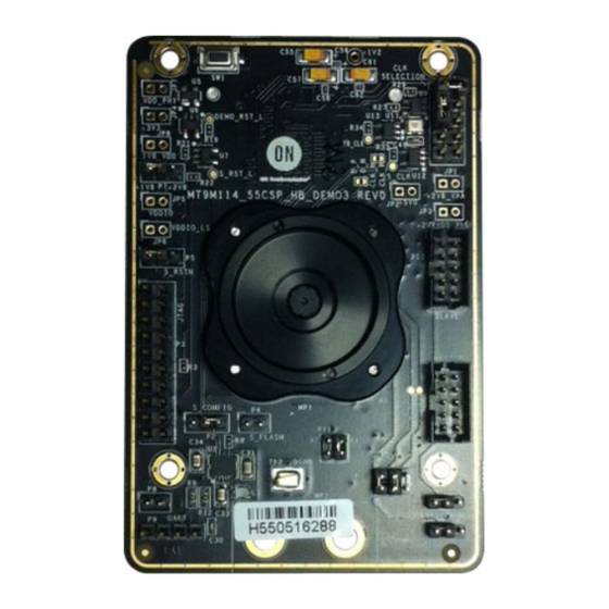
Figure 1. MT9M114 Evaluation Board
1
www.onsemi.com
Publication Order Number:
EVBUM2524/D
Advertisement
Table of Contents

Related Manuals for ON Semiconductor MT9M114EBLSTCZH3-GEVB


Summary of Contents for ON Semiconductor MT9M114EBLSTCZH3-GEVB
- Page 1 Evaluation Board Overview The evaluation boards are designed to demonstrate the features of www.onsemi.com ON Semiconductor’s image sensors products. This headboard is intended to plug directly into the Demo3 system. Test points and EVAL BOARD USER’S MANUAL jumpers on the board provide access to the clock, I/Os, and other miscellaneous signals.
- Page 2 MT9M114EBLSTCZH3−GEVB Top View RESET Switch SW1 CLK_SELECT P32 VDDIO_SELECT P7 TRST P5 SLAVE I C HEADER P13 JTAG P3 MASTER I C HEADER P12 CONFIG P2 EEPROM_ADDR_SEL P11 C M/S P15 FLASH P4 UART ENABLE P8 SADDR P6 UART P9 PARALLEL OUT EN P1 Figure 3.
- Page 3 MT9M114EBLSTCZH3−GEVB Jumper Pin Locations The jumpers on headboards start with Pin 1 on the leftmost side of the pin. Grouped jumpers increase in pin size with each jumper added. The ‘L’ shape denotes pin 1. Pin 1 Pins 1−4 Figure 5. Pin Locations for a Single Jumper. Pin 1 is Located at the Leftmost Side and Increases as it Moves to the Right (Except for P11) Pin 1 Pins 1 &...
- Page 4 Single Camera; External Clock from Demo3 5−6 Single Camera; External Clock from Demo3 Interfacing to ON Semiconductor Demo3 Baseboard Table 2. SHORTENED JUMPERS FOR POWER The ON Semiconductor Demo3 headboard has a similar MEASUREMENT 52-pin connector which mates P5 of the Demo3 baseboard. Jumper Voltage...
- Page 5 onsemi, , and other names, marks, and brands are registered and/or common law trademarks of Semiconductor Components Industries, LLC dba “onsemi” or its affiliates and/or subsidiaries in the United States and/or other countries. onsemi owns the rights to a number of patents, trademarks, copyrights, trade secrets, and other intellectual property. A listing of onsemi’s product/patent coverage may be accessed at www.onsemi.com/site/pdf/Patent−Marking.pdf.
Need help?
Do you have a question about the MT9M114EBLSTCZH3-GEVB and is the answer not in the manual?
Questions and answers