
Related Manuals for Xycom XVME 200

Summary of Contents for Xycom XVME 200
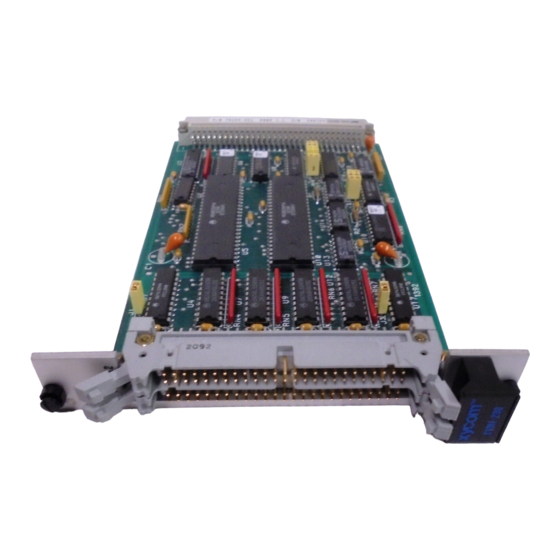
- Page 5 XVME-200/290 Manual December, 1987 Chapter INTRODUCTION OVERVIEW The XVME-200 and XVME-290 are Digital I/O VMEbus compatible boards (also is a single-high (3U), single-wide referred to as DIO Modules). XVME-200 module, and the XVME-90 is a double-high (6U), single-wide form factored modules. The DIO Module provides a VME system with 32 digital (TTL) I/O channels, full VMEbus interrupt capability, and port handshake control features.
- Page 6 XVME-200/290 and the 68230 PI/T device, a manual kit is being shipped with the XVME-200/290 DIO Module (the manual kit is referenced as XYCOM Part #74200-001). This kit consists of two parts: a *Motorola MC68230 M a n u a l ( c ) ( r e f e r e n c e d a s X Y C O M P a r t #74200-003), a n d a n XVME-200/290 M a n u a l (referenced as XYCOM Part #74200-002.
- Page 9 XVME-200/290 Manual December, 1987 The DIO Module uses two 68230 Parallel Interface/Timer devices to provide a total of 32 parallel I/O lines (16 lines per chip) arranged as four I/O ports (two 8 line ports per chip), as well as 2 programmable timers (1 timer per chip). Several different operating modes can be programmed for the parallel ports and timers, to provide a high degree of versatility and flexibility.
-
Page 10: Module Specifications
XVME-200/290 Manual * December, 1987 MODULE SPECIFICATIONS The following is a list of the operational and environmental specifications for the XVME-200/290 DIO Module. - Page 11 XVME-200/290 Manual December, 1987 Table l-l. Digital I/O Module Specifications Specification Characteristic Number of Channels 68230 (2 per module) Parallel Interface Device V il = 0.8V max., Iil = -750 max. Input Characteristics V ih = min., lil= -325 2.0v uA max.
- Page 12 XVME-200/290 Manual December, 1987 VMEbus Compliance Complies with VMEbus Standard Rev. C.l A 16:D8(0) DTB Slave I(1) to I(7) interrupter (STAT) with programmable interrupt vector Size - Single (XVME-200 Size - Double (XVME-290) Base address jumper-selectable on 1K boundaries within the VMEbus short I/O address space...
-
Page 13: Installation
XVME-200/290; and a controller subsystem module which employs a Data Transfer Bus Arbiter, a System Clock driver, a System Reset driver, and a Bus timeout module. (The XYCOM XVME-010 System Resource Module provides a controller subsystem with the components listed.) A host processor module which incorporates an on-board controller sub- system (such as XYCOM’s... - Page 17 XVME-200/290 Manual December, 1987 XVME-200/290 DIO MODULE JUMPER LIST Table 2-1. DIO Module Jumper List Jumper Jl and J3 Determine the direction of handshake line H2 for both of the PI/T chips (refer to Section 2.4.5 of this manual). Determines whether the module will respond to supervisory or non-privileged short I/O VMEbus cycles (refer to Section 2.4.2 of this manual).
- Page 18 XVME-200/290 Manual December, 1987 Table 2-2. Base Address Jumper Options (Cont’d) Base Address of JA15 JA14 JA13 JA12 JAll JAlO Module 3400H 3800H 3COOH 4000H 4400H 4800H 4COOH 5000H 5400H 5800H 5COOH 6OOOH 6400H 6800H 6COOH 7000H 7400H 7800H 7COOH 8OOOH 8400H 8800H...
- Page 19 XVME-200/290 Manual December, 1987 Table 2-2. Base Address Jumper Options (Cont’d) Base Address of JAI3 JA12 JAI1 JAI0 JA15 JA14 Module E800H EC00H F000H F400H F8OOH FC00H 2.4.2 Address Modifier Jumper The DIO Module has one jumper that determines which Address Modifier Codes it will respond to.
- Page 20 XVME-200/290 Manual December, 1987 2.4.3 Interrupt Level Selection Jumpers The DIO Module can either be configured to generate VMEbus interrupts at levels 1-7 or the module interrupt capability can be completely disabled. Table 2-4 shows how jumpers JAI-JA3 are used to determine the interrupt level status for the DIO Module.
-
Page 21: Connector Pin Assignments
XVME-200/290 Manual December, 1987 In these modes, the direction of two of the handshake pins (H2 and H4) should be programmable. However, due to constraints in hardware design, pin H4 must always be programmed as an output. Thus, pin H2 may be programmed as either an input or an output depending on what type of handshake protocol is to be used. - Page 22 XVME-200/290 Manual December, 1987 The XVME-290 Module I/O interconnect is done via P2 of the VMEbus backplane (XVME-290/l) or through two 50-pin connectors (JKl and JK2) mounted in the P2 area (XVME-290/2). On the XVME-290/l, P2 carries all the signals for both PI/T #1 and while for the XVME-290/2, JKl carries signals for PI/T #l and JK2 PI/T #2,...
- Page 24 XVME-200/290 Manual December, 1987 2.5.2 Pl and P2 Connectors Connectors PI and P2 are mounted at the rear edge of the board (see Figure 2-1). The pin connections for ( a 96-pin, 3-row connector) contains the standard address, data, and control signals necessary for the operation of VMEbus-defined NEXP modules.
- Page 25 XVME-200/290 Manual December, 1987 Table 2-7. Pin Assignment for P2 (XVME-290/l Only) ROW A ROW B ROW C Pin # Signal Pin # Signal Pin # Signal P2A-1 H4 OUT-1 P2B- 1 v c c P2C-1 G N D P2A-2 TMR OUT-1 P2B-2 G N D...
-
Page 26: Module Installation
XVME-200/290 Manual December, 1987 2.6 MODULE INSTALLATION XYCOM XVME modules are designed to comply with all physical and electrical VMEbus backplane specifications. The XVME-200 DIO Module is a single-high, single-wide VMEbus module, and as such, only requires the Pl backplane. - Page 27 XVME-200/290 Manual December, 1987 Once the board is properly seated, it should be secured to the chassis by tightening the two machine screws at the extreme top and bottom of the board. 2-15...
-
Page 28: Module Programming
XVME 200/290 Manual December, 1987 Chapter 3 MODULE PROGRAMMING INTRODUCTION This chapter will briefly examine the addressing, and initialization procedures and constraints required when programming the XVME-200 and XVME-290 DIO Modules. In order to demonstrate the correct sequence of initialization for the ports and registers contained in the 68230 PI/T chips, two programming examples (with comments) have been incorporated in this chapter. - Page 29 XVME-2001290 Manual December, 1987 Address Table 3-l. Register Offsets From the Module Base 68230 PI/T Register Offsets from Module Base Address PI/T #l PI/T #2 DEC HEX DEC HEX PI/T Register Name Port General Control Register Port Service Request Register Port A Data Direction Register Port B Data Direction Register Port C Data Direction Register...
- Page 30 XVME-200/290 Manual December, 1987 A specific register address in one of the 68230 chips can be accessed by simply adding the specific register offset to the module base address. For example, the offset specified for the Port General Control Register for PI/T #2 is 41H, and if the module base address is jumpered to 1000H, the register can be accessed at 1041H.
- Page 32 XVME-200/290 Manual December, 1987 MODULE VMEbus INTERRUPT CAPABILITY Four sources of interrupts exist on the XVME-200 and the XVME-290. These are When the timer and port interrupt sources from both PI/T #l and PI/T #2. enabled, each of the four interrupt sources can generate VMEbus interrupts on the level selected by jumpers JAI-JA3 (refer to Section 2.4.3 of this manual).
- Page 33 XVME-200/290 Manual December, 1987 PC7/TIACK PC6/PIACK PIRQ TINTEN PC3/TOUT PCZ/TIN PORT B PORT A Input output output output Input output output Input Figure 3-3. Port C/Alternate Function Signal Definitions The following is a brief explanation of each PORT C bit: 0 and 1 are used to control the direction of the 8-bit data Bits...
- Page 34 XVME-200/290 Manual December, 1987 During a VMEbus reset, all three PI/T ports (A, B, & C) assume an input direction. Pull-up resistors present on bits PC0 and PC1 cause the port A and B data line transceivers to assume an input direction. Pull-up resistors also cause PORT C pins 3, 4, and 5 to go high at reset, thereby preventing the possibility of unintentional interrupts (port or timer).
- Page 35 XVME-200/290 Manual December, 1987 PI/T Timer Interrupt Enabling 3.3.1.3 68230 timer interrupts are enabled/disabled via PORT C output pin PC4. When PC4 is negated (logic ‘l”), the timer cannot generate VMEbus interrupts. When PC4 is asserted (logic “0”), the timer will generate VMEbus interrupts. When the timer interrupts are to be used, PORT C pins PC3/TOUT and PC7/TIACK must be programmed to serve the timer interrupt request and acknowledge functions.
- Page 36 XVME-200/290 Manual December, 1987 Table 3-3 shows how pins and PC1 affect the direction of the PORT A and B data transceivers. Remember, each PI/T chip has its own PORT A and B, and thus there is a total of 4 lines which are used to control the direction of the four data transceivers (refer to the Module Block Diagram, Figure l-l).
- Page 37 XVME-200/290 Manual December, 1987 PROGRAMMKNG EXAMPLES The two 68000 CPU code programming examples which follow, demonstrate general methods of initialization of the 68230 PI/T devices on the XVME-200 and XVME-290 Modules. The following equates will be used in both examples: ;...
- Page 38 XVME-200/290 Manual December, 1987 E x a m p l e #l * Basic Set Up: PI/T #l Mode 0 = Unidirectional 8-bit Mode Submode 1X = Bit I/O (Pin-Definable Single-Buffered Output or Non-Latched Input) Goals: Port A, all bits = non-latched inputs.
- Page 39 XVME-200/290 Manual December, 1987 M0VE.B #$AS,PBCR(AO) ; Initialize Port B ; Submode 1X ; H4 = asserted output ; H3 & H4 interrupts disabled ; PC4 = Port C function M0VE.B #$18,PSRR(AO) ; PCS/PIRQ = PIRQ function ; PC6/PIACK = PIACK function ;...
- Page 40 XVME-200/290 Manual December, 1987 16) Vectored interrupts are supported. 17) When zero is detected, the counter will generate a VMEbus interrupt, reload the counter, and continue counting. Hl, H2, H3, and timer interrupts are enabled. CODE: A0 = base address of PI/T #l M0VEA.L #PI/T2BASE,AO Disable timer M0VE.B #O,TCR( AO)
- Page 41 XVME-200/290 Manual December, 1987 M0VE.B #CHIGH,CPRH(AO) ; Initialize counter preload registers M0VE.B #CMID,CPRM(AO) M0VE.B #CLOW,CPRL(AO) M0VE.B #TVCTR,TIVR(AO) ; Initialize timer IACK vector ; Set PC4 = 0 to enable timer interrupts BCLR#4,PCDR(AO) ; Enable timer BSET#O,TCR(AO) 3-14...
- Page 42 XVME-200/290 Manual December, 1987 Appendix A VMEbus CONNECTOR/PIN DESCRIPTION The XVME-200 and XVME-290 Modules are VMEbus compatible boards. There is one 96-pin bus connector on the rear edge of the board labeled Pl (refer to Chapter 2, Figure 2-1 for the location) and the XVME-290/l also uses the P2 connector.
- Page 43 XVME-200/290 Manual December, 1987 Table A-l. VMEbus Signal Identification (cont’d) Connector Signal Pin Number Signal Name and Description Mnemonic A0l-A23 A:24-30 ADDRESS BUS (bits l-23): Three-state driven address lines that specify a memory address. lC:15-30 A24-A31 ADDRESS BUS (bits 24-31): Three-state driven bus 2B:4-11 expansion address lines.
- Page 44 XVME-200/290 Manual December, 1987 Table A-l. VMEbus Signal Identification (cont’d) Connector Signal Mnemonic Pin Number Signal Name and Description BR0*-BR3* lB:12-15 BUS REQUEST (0-3): Open-collector driven signals generated by Requesters. These signals indicate that a DTB master in the daisy-chain requires access to the bus.
- Page 45 XVME-200/290 Manual December, 1987 Table A-l. VMEbus Signal Identification (cont’d) Connector Signal Signal Name and Description Mnemonic Pin Number 1A:20 INTERRUPT ACKNOWLEDGE: Open-collector or three- IACK* state driven signal from any master processing an It is routed via the backplane to interrupt request.
- Page 46 XVME-200/290 Manual December, 1987 Table A-l. VMEbus Signal Identification (cont’d) Connector Signal Mnemonic Pin Number Signal Name and Description SYSFAIL* 1C:l0 SYSTEM FAIL: Open-collector driven signal that indicates that a failure has occurred in the system. It may be generated by any module on the VMEbus. lC:12 SYSRESET* SYSTEM RESET: Open-collector driven signal which,...
- Page 47 XVME-200/290 Manual December, 1987 BACKPLANE CONNECTOR Pl T h e f o l l o w i n g t a b l e l i s t s t h e Pl p i n a s s i g n m e n t s b y p i n n u m b e r o r d e r . (The connector consists of three rows of pins labeled rows A, B, and C.) Table A-2.
- Page 48 XVME-200/290 Manual December, 1987 Table A-3. Pin Assignment for P2 (XVME-290/l Only) ROW A ROW B ROW C Pin # Pin # Signal Pin # Signal Signal P2A-1 H4 OUT-l P2B-1 v c c P2C-1 P2A-2 TMR OUT-1 P2B2 G N D P2C-2 H2 OUT-l P2A-3...
Need help?
Do you have a question about the XVME 200 and is the answer not in the manual?
Questions and answers