Table of Contents
Advertisement
Quick Links
This user's guide describes the characteristics, operation, and use of the TPS22924EVM-532 evaluation
module (EVM). This EVM demonstrates the Texas Instruments TPS22924 load switch with controlled turn
on. The input voltage range of the TPS22924 is 0.75 V to 3.6 V. An integrated charge pump biases the
NMOS switch to achieve a minimum switch ON resistance. The switch is controlled by an on/off input
(EN), which is capable of interfacing directly with low-voltage control signals. This user's guide includes
setup instructions, schematic diagram, bill of materials, and printed-circuit board layout drawings for the
EVM.
1
Introduction
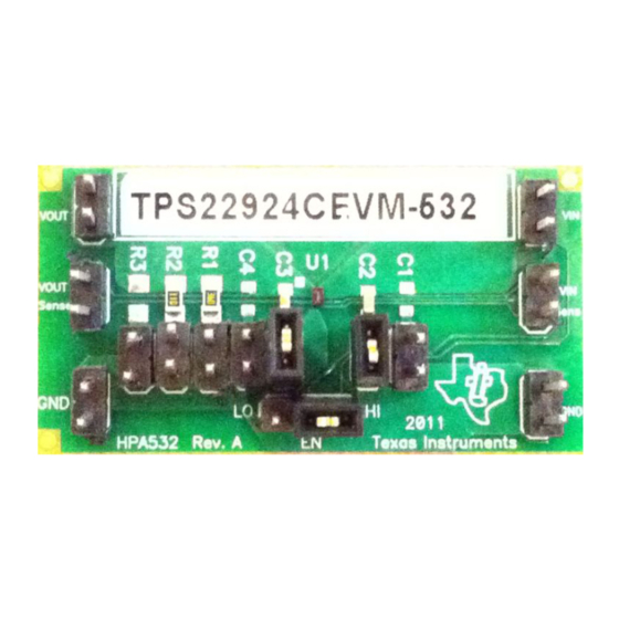
The TPS22924EVM-532 evaluation module (EVM) helps designers evaluate the operation and
performance of the TPS22924 load switch. The board features the small 6-pin CSP package for a small
solution size.
EVM
HPA532-001
HPA532-002
1.1
Related Documentation From Texas Instruments
TPS22924, ULTRA-SMALL, LOW-INPUT-VOLTAGE, LOW r
2
Setup
This section describes the jumpers and connectors on the EVM as well as how to properly connect, set
up, and use the TPS22924EVM-532.
2.1
J1/J3 – Input Connections
This is the connection for the leads from the input source. Connect the positive connection to the VIN J1
and the negative connection to the GND J3.
2.2
J4/J6 – Output Connections
This is the connection for the output of the TPS22924EVM. Connect the positive connection of the load to
the VOUT J4 and the negative connection to the GND J6.
2.3
JP3 – EN
This is the enable input for the device. Place a shorting jumper across the HI and EN pins of JP3 to
enable the integrated circuit (IC). Place a shorting jumper across the LO and EN pins of JP3 to disable the
IC. A shorting jumper must be installed on JP3 in either the ON or OFF positions, and EN must not be left
unconnected. An external enable source can be applied to the TPS22924 by removing the shunt and
connecting a signal to the center pin of JP3. EN ≥ 0.75V is required for the ACTIVE or ON state of the
device. A switching signal may also be used and connected at this point.
SLVU456A – May 2011 – Revised June 2011
Submit Documentation Feedback
Table 1. TPS22924 VOUT Rise Time Options
DEVICE
TPS22924B
TPS22924C
Copyright © 2011, Texas Instruments Incorporated
SLVU456A – May 2011 – Revised June 2011
TPS22924EVM-532
Rise Time (µS) Typ.
100
840
LOAD SWITCH data sheet (SLVSA52)
ON
User's Guide
VIN(V)
3.6
3.6
TPS22924EVM-532
1
Advertisement
Table of Contents

Related Manuals for Texas Instruments TPS22924EVM-532


Summary of Contents for Texas Instruments TPS22924EVM-532
- Page 1 SLVU456A – May 2011 – Revised June 2011 TPS22924EVM-532 This user's guide describes the characteristics, operation, and use of the TPS22924EVM-532 evaluation module (EVM). This EVM demonstrates the Texas Instruments TPS22924 load switch with controlled turn on. The input voltage range of the TPS22924 is 0.75 V to 3.6 V. An integrated charge pump biases the NMOS switch to achieve a minimum switch ON resistance.
-
Page 2: Operation
See the Typical Characteristics section of the TPS22924 data sheet. Board Layout, Schematic, and Bill of Materials This section provides the TPS22924EVM-532 board layout, schematic, and bill of materials. Board Layout For best performance, all traces should be as short as possible. To be most effective, the input and output capacitors should be placed close to the device to minimize the effects that parasitic trace inductances may have on normal and short-circuit operation. - Page 3 Board Layout, Schematic, and Bill of Materials www.ti.com Figure 1. Top Assembly Layer Figure 2. Top Layer SLVU456A – May 2011 – Revised June 2011 TPS22924EVM-532 Submit Documentation Feedback Copyright © 2011, Texas Instruments Incorporated...
-
Page 4: Schematic And Bill Of Materials
Install label in silkscreened box after final wash. Text shall be 8 point font. Text shall be per Table 3 Table 3. Assembly Number Text HPA532-001 TPS22924BEVM-001 HPA532-002 TPS22924CEVM-002 SLVU456A – May 2011 – Revised June 2011 TPS22924EVM-532 Submit Documentation Feedback Copyright © 2011, Texas Instruments Incorporated... - Page 5 Board Layout, Schematic, and Bill of Materials www.ti.com 5.3 VOUT Rise Time and TON Response Figure 4. TPS22924B TON and Trise Example SLVU456A – May 2011 – Revised June 2011 TPS22924EVM-532 Submit Documentation Feedback Copyright © 2011, Texas Instruments Incorporated...
- Page 6 Board Layout, Schematic, and Bill of Materials www.ti.com Figure 5. TPS22924C TON and Trise Example SLVU456A – May 2011 – Revised June 2011 TPS22924EVM-532 Submit Documentation Feedback Copyright © 2011, Texas Instruments Incorporated...
-
Page 7: Evaluation Board/Kit Important Notice
Evaluation Board/Kit Important Notice Texas Instruments (TI) provides the enclosed product(s) under the following conditions: This evaluation board/kit is intended for use for ENGINEERING DEVELOPMENT, DEMONSTRATION, OR EVALUATION PURPOSES ONLY and is not considered by TI to be a finished end-product fit for general consumer use. Persons handling the product(s) must have electronics training and observe good engineering practice standards. -
Page 8: Important Notice
IMPORTANT NOTICE Texas Instruments Incorporated and its subsidiaries (TI) reserve the right to make corrections, modifications, enhancements, improvements, and other changes to its products and services at any time and to discontinue any product or service without notice. Customers should obtain the latest relevant information before placing orders and should verify that such information is current and complete. -
Page 9: Texas Instruments
Mouser Electronics Authorized Distributor Click to View Pricing, Inventory, Delivery & Lifecycle Information: Texas Instruments TPS22924CEVM-532...
Need help?
Do you have a question about the TPS22924EVM-532 and is the answer not in the manual?
Questions and answers