Table of Contents
Advertisement
Quick Links
Advertisement
Table of Contents

Related Manuals for Inrevium VIRTEX-5 TB-5V-LX110/220/330-DDR2

Summary of Contents for Inrevium VIRTEX-5 TB-5V-LX110/220/330-DDR2
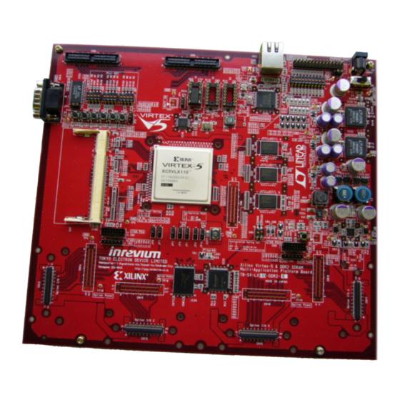
- Page 1 TB-5V-LX110/220/330-DDR2 VIRTEX-5 Multi-Application Platform Board TB-5V-LX110/220/330-DDR2 Hardware User Guide Rev2.1 (Simple Version) 1, Higashikata-cho, Tsuzuki-ku Yokohama-City, Kanagawa, Japan 224-0045 E-mail: x2bdg@teldevice.co.jp...
-
Page 2: Table Of Contents
TB-5V-LX110/220/330-DDR2Hardware User Guide Rev2.1s Table of Contents 1. Accessories ..........................3 2. Precautions..........................3 3. Overview ..........................4 4. Feature ............................. 4 5. Block Diagram ......................... 5 6. External View ........................... 6 7. Board Specification......................... 6 8. Board Components ......................... 7 Power Connector and Power Module .................. -
Page 3: Accessories
TB-5V-LX110/220/330-DDR2Hardware User Guide Rev2.1s 1. Accessories ■ 12V 4A AC Adaptor ■ User’s Manual ■ Board Mounting Leg ■ TE7725 Download Cable (TD-LB2CABLE ,USB Cable and Flying Wire) 2. Precautions ■ Product and information contained in this manual is subject to change without prior notice for improvement. -
Page 4: Overview
TB-5V-LX110/220/330-DDR2Hardware User Guide Rev2.1s 3. Overview TB-5V-LX110/220/330-DDR2 is an evaluation board that is equipped with high density, high performance Viretex-5 LX series, DDR2 SDRAM chip and DDR2 SO-DIMM socket. Users can evaluate high speed memory interface and wide variety of application using this board series. -
Page 5: Block Diagram
TB-5V-LX110/220/330-DDR2Hardware User Guide Rev2.1s 5. Block Diagram JTAG Data,DQS PC4 & PinHeader Flash Rom ADR,CLK,Command JTAG Config Chip PC4 & TE7725PF PinHeader ADR,CLK,Command DDR2 Data,DQS 512M UART LTC1348 9pin D-SUB Virtex5 Soft tuch CN LX110 25MHz LX220 DDR2 Data,DQS Addr, 512M Data TD,RD... -
Page 6: External View
TB-5V-LX110/220/330-DDR2Hardware User Guide Rev2.1s 6. External View OSC Socket P.13 10/100 Base Ethernet P.25 General I/O Pin Header P.40 LVDS I/O Connect P.27 VBATT_0 Level Setting P.54 User DipSW P.15 PLL Setting DipSW P.14 User LED P.16 LVDS I/O Power Setting P.11 Power SW RS-232C Port P.17 Power Status LED 1.0V P.8... -
Page 7: Board Components
TB-5V-LX110/220/330-DDR2Hardware User Guide Rev2.1s 8. Board Components Power Connector and Power Module Single 12V power is externally supplied from the AC adaptor that comes with the board. Figure.3 AC Adopter connection Power Supply Connections AC ADAPTER 12V Switch LTM4600EV LTM4600EV LTC3728LEUH-1 1.0V 1.8V... -
Page 8: Power Status Led
TB-5V-LX110/220/330-DDR2Hardware User Guide Rev2.1s Power Status LED Power Status LEDs (LED5, LED7, LED10, LED13 and LED19) indicate that the power supply is running normally. Ensure that all Leeds are turned on, otherwise something is wrong with the board. Switch off the power supply since there may be a short circuit between the FPGA user circuit and device. -
Page 9: Power Voltage Selector For I/O Connectors
TB-5V-LX110/220/330-DDR2Hardware User Guide Rev2.1s Power Voltage Selector for I/O connectors It is possible to select 2.5V or 3.3V for VCCO power voltage of option I/O connectors. ■ Bank4, Bank6, Bank21, Bank22, Bank25, Bank26 Connected to: Option I/O connector Set each jumper to the desired power voltage (2.5V or 3.3V) in accordance with interface level. 2.5V Setting 3.3V Setting *JP1 is the jumper for Configuration Mode (P.68) -
Page 10: Power Voltage Selector For Lvds Connectors
TB-5V-LX110/220/330-DDR2Hardware User Guide Rev2.1s Power Voltage Selector for LVDS connectors It is possible to select 2.5V or 3.3V for VCCO power voltage of LVDS connectors. ■ Bank20, Bank24 Connected to: LVDS I/O connector Set jumper to the desired power voltage (2.5V or 3.3V) in accordance with interface level using JP3. -
Page 11: Power Voltage Selector For I/O Pin Header Connectors
TB-5V-LX110/220/330-DDR2Hardware User Guide Rev2.1s Power Voltage Selector for I/O pin header connectors It is possible to select 2.5V or 3.3V for VCCO power voltage of LVDS connectors. ■ Bank19 Connected to: Pin header I/O connector, User DIP switch, User Push switch Set jumper to the desired power voltage (2.5V or 3.3V) in accordance with interface level using JP12. -
Page 12: Oscillator
TB-5V-LX110/220/330-DDR2Hardware User Guide Rev2.1s Oscillator The board is provided with one differential LV-PECL PLLIC (DIP switch setting for variable frequency) and two oscillator sockets that are connected to the FPGA’s GCLK pin. Be sure to set the 16MHz oscillator that comes with the board to a correct pin position of the oscillator socket (X1) that is connected to the PLLIC. -
Page 13: Pllic (Ics8430-61) Setting
TB-5V-LX110/220/330-DDR2Hardware User Guide Rev2.1s PLLIC (ICS8430-61) Setting DIP switches SW5 to SW7 are used to set output frequency of PLLIC. Output frequency can be obtained in the following formula. Fout = (fxtal/16)x(M/N) Be sure to set it so that internal VCO frequency fvco((fxtal/16)x M) is within a range of 250 - 500MHz. *Ex) M=250/N=2 setting generates 125MHz clock. -
Page 14: User Dip Switch
TB-5V-LX110/220/330-DDR2Hardware User Guide Rev2.1s User DIP Switch A 10bit DIP switch is connected to the I/O of FPGA. Set the switch to ON to set High. The signal level is changed 2.5 or 3.3V according to Pin Header. ON: Output “High” OFF: Output ”Low”... -
Page 15: Rs-232C Port
TB-5V-LX110/220/330-DDR2Hardware User Guide Rev2.1s RS-232C Port This connecter can transfer Tx/Rx data from user function and CPU program with connecting with PC. (Then the cable is used “Cross Cable” that is available commercially.) RS232C RS232C FPGA Driver Connector Virtex-5 LTC1348 9-pin D-Sub Figure.14 RS-232C Block Diagram Figure.15 RS-232C... -
Page 16: Ddr2 Sdram So-Dimm Socket
TB-5V-LX110/220/330-DDR2Hardware User Guide Rev2.1s DDR2 SDRAM SO-DIMM Socket DDR2 SO-DIMM socket is mounted on this board. (It is possible to use up to 2GB DDR2 SO-DIMM) Figure.17 DDR2 SDRAM SO-DIMM Socket 4, 2007 (Rev 2.1s) 16/26... -
Page 17: Ddr2 Sdram Memory Component
TB-5V-LX110/220/330-DDR2Hardware User Guide Rev2.1s DDR2 SDRAM Memory Component Three pieces of DDR2 SDRAM component (512Mb) is used on this board (Two Configurations). The connection between FPGA and memories is shown like Figure.19. Also Soft-touch connector that is produced by Agilent Technology is mounted between FPGA and IC29 so it’s possible to confirm each signal using Agilent’s Logic Analyzer. -
Page 18: 10/100 Base Ethernet
TB-5V-LX110/220/330-DDR2Hardware User Guide Rev2.1s 10/100 Base Ethernet Ethernet controller (LAN9118) is mounted on this board so it is possible to communicate 10/100Base Ethernet with PC via RJ-45 connector. RJ-45 LAN9118 Figure.20 RJ-45 connector and Ethernet controller LVDS I/O Connector For high speed data access, two channels (Tx/ Rx) of LVDS connectors are mounted on this board. There are 20 pair of data lines and 2 pair of clock line for each channel. -
Page 19: Multi-Purpose I/O Pin Header
TB-5V-LX110/220/330-DDR2Hardware User Guide Rev2.1s Multi-Purpose I/O Pin Header It is possible to change the signal level to 2.5 or 3.3V according to connected interface. Figure.23 Multi- Purpose I/O Pin Header Soft-Touch Connector Soft-Touch Connector produced by Agilent Technology is mounted between FPGA and DDR2 SDRAM (IC29), and between FPGA and Option I/O connectors (CN12, 13, 16, 17) on this board as the following picture. - Page 20 TB-5V-LX110/220/330-DDR2Hardware User Guide Rev2.1s Flash memory Sector Selection Setting The setting of SW15 can select to a programming section of flash memory. For this feature, it is possible to program multiple data and to select several configuration data. Figure.31 Flash memory Sector Selection Switch (SW15) SW15 Flash Memory Region 16Mbit Flash All Region(Top Sector)
-
Page 21: Others
TB-5V-LX110/220/330-DDR2Hardware User Guide Rev2.1s VBATT_0 Level Setting Virtex-5 has the function of configuration encryption. If encryption is used, it needs to provide a power supply to VBATT. It is possible to change the power supply of VBATT_0 (R29) of FPGA to ‘H’ (3.3V) or ‘L’ (GND) using JP4. -
Page 22: How To Program To A Device
TB-5V-LX110/220/330-DDR2Hardware User Guide Rev2.1s 9. How to program to a device Configuration Brief Overview See the following diagram about configuration structure. It is possible to program to flash memory using a TD-LB2CABLE (attached in this board) or Parallel Cable (III or IV). First, programmming a configuration file (MCS) to flash memory using each download cable. - Page 23 TB-5V-LX110/220/330-DDR2Hardware User Guide Rev2.1s CN3 PC4) CN4 (PC3) Figure.35 JTAG Connector Or it is possible to program to FPGA directly via CN1 or CN2. JTAG CN1(PC4) FPGA Virtex-5 CN2PC3 CN2 (PC3) CN1 (PC4) Figure.36 Configuration Structure 2 4, 2007 (Rev 2.1s) 23/26...
- Page 24 TB-5V-LX110/220/330-DDR2Hardware User Guide Rev2.1s FPGA Configuration The following 1) ~ 4) are descriptions of FPGA configuration. 1) Set JP1 “BPI UP” mode. *Note: JP2, 6, 7, 8, 9, 10 are jumpers for power supply setting of I/O Banks. (Page.9) Figure.59 BPI UP Mode Setting 2) Set SW3 as Figure.60 and power on the board.
- Page 25 TB-5V-LX110/220/330-DDR2Hardware User Guide Rev2.1s 3) If FPGA configuration is completed, LED2 (Green) will light. Configuration completed. Figure.61 DONE LED 4) If Reconfiguration bottom (SW2) is pushed, start a reconfiguration of FPGA. Figure.62 Reconfiguration Bottom 4, 2007 (Rev 2.1s) 25/26...
- Page 26 No one is permitted to reproduce or duplicate the whole or part this document without approval from Tokyo Electron Device Limited. Inquiries:PLD Solution Product Group E-mail:x2bdg@teldevice.co.jp URL: http://ppg.teldevice.co.jp/ (Japanese Site) http://www.inrevium.jp/eng/ (English Site) 4, 2007 (Rev 2.1s) 26/26...
Need help?
Do you have a question about the VIRTEX-5 TB-5V-LX110/220/330-DDR2 and is the answer not in the manual?
Questions and answers