Table of Contents
Advertisement
Quick Links
Advertisement
Table of Contents

Related Manuals for Multitech MultiConnect MTPCIE-EV3


Summary of Contents for Multitech MultiConnect MTPCIE-EV3
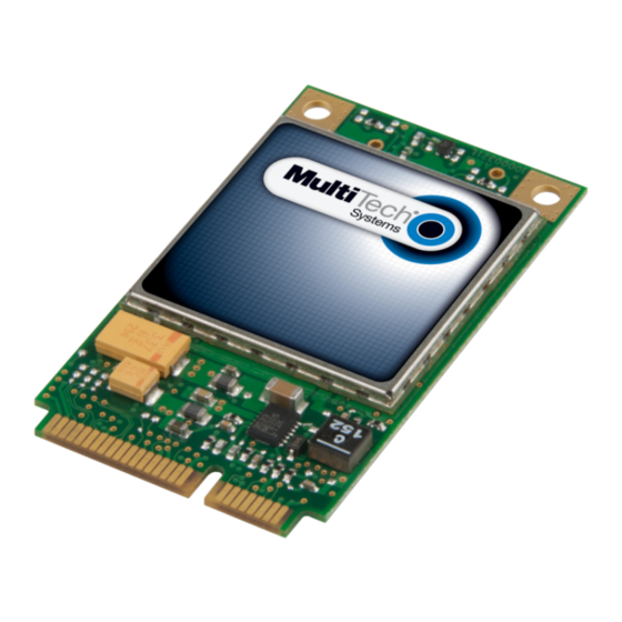
- Page 1 ® MultiConnect PCIe MTPCIE-EV3 Developer Guide...
- Page 2 Legal Notices The MultiTech products are not designed, manufactured or intended for use, and should not be used, or sold or re-sold for use, in connection with applications requiring fail-safe performance or in applications where the failure of the products would reasonably be expected to result in personal injury or death, significant property damage, or serious physical or environmental damage.
-
Page 3: Table Of Contents
CONTENTS Contents Chapter 1 – Product Overview ..........................6 About MultiConnect PCIe.............................. 6 Documentation ................................6 Product Build Options ..............................6 Developer Kit Contents ..............................7 Chapter 2 – Pinout ..............................8 Multi-Tech Mini PCIe Pinout ............................8 Standard Mini-PCI Express Pinout ..........................10 Chapter 3 –... - Page 4 CONTENTS Host Labeling................................35 Chapter 13 – Regulatory Statements........................36 47 CFR Part 15 Regulation Class B Devices ......................... 36 Industry Canada Class B Notice........................... 36 Requirements for Cellular Antennas with regard to FCC/IC Compliance ..............36 Chapter 14 – Environmental Notices ........................37 Waste Electrical and Electronic Equipment Statement ....................
- Page 5 CONTENTS read()..................................58 write()..................................58 close()..................................59 Test Program() ................................60 Index..................................62 ® MultiConnect PCIe MTPCIE-EV3 Developer Guide...
-
Page 6: Chapter 1 - Product Overview
PRODUCT OVERVIEW Chapter 1 – Product Overview About MultiConnect PCIe Documentation Download the following documentation at www.multitech.com/setup/product.go. Document Description MultiConnect PCIe Developer This document. Provides an overview, safety and regulatory information, Guide developer board schematics and pinouts, and device. USB Driver Installation Guide Provides instructions for installing USB drivers on Linux and Windows systems (part number S000569). -
Page 7: Developer Kit Contents
PRODUCT OVERVIEW Developer Kit Contents Your Developer Kit (MTPCIE-DK1) includes the following: Developer Board 1 - MTPCIE-DK1 Developer Board Power Supply 1 - 100-240V 9V-1.7A power supply with removable blades, 1 - US blade/plug, 1 - EURO blade/plug, 1 - UK blade/plug Cables 1 - RS-232 DE9F-DE9M serial cable, 1 - RJ-45 Ethernet cable, 2 -USB cable 2 - SMA-to-UFL antenna cables (1 - for cellular, 1 - for GPS) 1 - RSMA-to-UFL antenna cable for... -
Page 8: Chapter 2 - Pinout
PINOUT Chapter 2 – Pinout Multi-Tech Mini PCIe Pinout Note: SDIO can operate up to 25Mhz. Treat the SDIO traces to Host like a bus and keep the bus length as short as possible. Multi-Tech recommends adding series termination resistors on all the SDIO traces. Pin # Name Function... - Page 9 PINOUT Pin # Name Function 3G_DVI_WA0 Unused Ground 3G_DVI_CLK Unused 3G_DVI_RX Unused Unused 3G_DVI_TX Unused Ground Ground USB_D- 3G USB Negative Data Ground USB_D+ 3G USB Positive Data 3.3Vaux 3.3Vaux Ground 3.3Vaux 3.3Vaux LED_WWAN# 3G Cellular STAT LED Output Ground Unused Unused GPIO_3...
-
Page 10: Standard Mini-Pci Express Pinout
PINOUT Standard Mini-PCI Express Pinout For reference only. Pin # Function Description WAKE# WAKE 3.3Vaux 3.3Vaux COEX1 Co-existence pin, not defined COEX2 Co-existence pin, not defined 1.5V 1.5V CLKREQ# CLKREQ# UIM_PWR UIM_PWR UIM_DATA UIM_DATA REFCLK+ PCI Express reference clock UIM_CLK UIM_CLK REFCLK- PCI Express reference clock... - Page 11 PINOUT Pin # Function Description SMB_DATA SMB_DATA PETp0 PCI Express transmitter differential pair signal USB_D- USB Negative Data USB_D+ USB Positive Data 3.3Vaux 3.3Vaux 3.3Vaux 3.3Vaux LED_WWAN# LED Output LED_WLAN# LED Output Reserved Reserved LED_WPAN# LED Output Reserved Reserved 1.5V 1.5V Reserved Reserved...
-
Page 12: Chapter 3 - Design Considerations
DESIGN CONSIDERATIONS Chapter 3 – Design Considerations Design Consideration When using the Multi-Tech MiniPCIe form factor: Consult your modem’s device guide for device dimensions. With the modem, the Multi-Tech Mini PCIe form factor exceeds the standard Mini PCIe maximum component height for top and bottom. If you need to install components under the module, use taller connectors to avoid conflict. -
Page 13: Electrostatic Discharge Control
Take precautions to avoid exposure to electrostatic discharge during handling. MultiTech uses and recommends that others use anti-static boxes that create a faraday cage (packaging designed to exclude electromagnetic fields). MultiTech recommends that you use our packaging when returning a product and when you ship your products to your customers. -
Page 14: Chapter 4 - Developer Board
DEVELOPER BOARD Chapter 4 – Developer Board This developer board drawing shows the major board components. ® MultiConnect PCIe MTPCIE-EV3 Developer Guide... - Page 15 DEVELOPER BOARD ® MultiConnect PCIe MTPCIE-EV3 Developer Guide...
-
Page 16: Chapter 5 - Assembly Diagram
ASSEMBLY DIAGRAM Chapter 5 – Assembly Diagram ® MultiConnect PCIe MTPCIE-EV3 Developer Guide... -
Page 17: Bottom
ASSEMBLY DIAGRAM Bottom ® MultiConnect PCIe MTPCIE-EV3 Developer Guide... -
Page 18: Chapter 6 - Developer Board Block Diagram
DEVELOPER BOARD BLOCK DIAGRAM Chapter 6 – Developer Board Block Diagram ® MultiConnect PCIe MTPCIE-EV3 Developer Guide... -
Page 19: Chapter 7 - Developer Board Schematics
DEVELOPER BOARD SCHEMATICS Chapter 7 – Developer Board Schematics ® MultiConnect PCIe MTPCIE-EV3 Developer Guide... - Page 20 DEVELOPER BOARD SCHEMATICS ® MultiConnect PCIe MTPCIE-EV3 Developer Guide...
- Page 21 DEVELOPER BOARD SCHEMATICS ® MultiConnect PCIe MTPCIE-EV3 Developer Guide...
- Page 22 DEVELOPER BOARD SCHEMATICS ® MultiConnect PCIe MTPCIE-EV3 Developer Guide...
- Page 23 DEVELOPER BOARD SCHEMATICS ® MultiConnect PCIe MTPCIE-EV3 Developer Guide...
- Page 24 DEVELOPER BOARD SCHEMATICS ® MultiConnect PCIe MTPCIE-EV3 Developer Guide...
- Page 25 DEVELOPER BOARD SCHEMATICS ® MultiConnect PCIe MTPCIE-EV3 Developer Guide...
- Page 26 DEVELOPER BOARD SCHEMATICS ® MultiConnect PCIe MTPCIE-EV3 Developer Guide...
- Page 27 DEVELOPER BOARD SCHEMATICS ® MultiConnect PCIe MTPCIE-EV3 Developer Guide...
-
Page 28: Chapter 8 - Board Components
BOARD COMPONENTS Chapter 8 – Board Components Note that MTPCIE-EV3 models do not include Bluetooth/WiFi. Jumper Description JP3, JP4, JP5, JP48 Selects CGND or GND for antenna holder grounding. Default is CGND. JP6 allows you to select either the internal 5V regulator (INT PWR) or to choose EXT 5V (EXT PWR). - Page 29 BOARD COMPONENTS Jumper Description JP88 May be used to manually reset PCIe Wi-Fi device by briefly installing and then removing a jumper. Default is no jumper installed. JP89 This jumper, when installed, connects power to PCIe device. JP90 Not used by PCIe device.This jumper, when installed, connects power to OCG-E device.
-
Page 30: Chapter 9 - Installing The Device And Antennas
INSTALLING THE DEVICE AND ANTENNAS Chapter 9 – Installing the Device and Antennas To install a device on the board: With the radio side down, slide the device into the J23 connector. Press down until the device snaps into the X3 connector clips. Optional. -
Page 31: Chapter 10 - Attaching Power Supply Blades
ATTACHING POWER SUPPLY BLADES Chapter 10 – Attaching Power Supply Blades Power Supply and Blades If your device shipped with a power cord, attach the blades for your region. Power Power Power Supply Power Supply with Supply no with NAM Supply with Power EU blade... -
Page 32: Chapter 11 - Safety Notices And Warnings
SAFETY NOTICES AND WARNINGS Chapter 11 – Safety Notices and Warnings The following safety statements may be relevant and required in the host product literature. Radio Frequency (RF) Safety Due to the possibility of radio frequency (RF) interference, it is important that you follow any special regulations regarding the use of radio equipment. -
Page 33: User Responsibility
Do not place the device alongside computer discs, credit or travel cards, or other magnetic media. The information contained on discs or cards may be affected by the device. Using accessories, such as antennas, that MultiTech has not authorized or that are not compliant with MultiTech's accessory specifications may invalidate the warranty. - Page 34 SAFETY NOTICES AND WARNINGS structures (the antenna) and the body of users. Qualification for distances closer than 20 cm (portable operation) would require re-certification. Wireless devices could generate radiation. Other nearby electronic devices, like microwave ovens, may also generate additional radiation to the user causing a higher level of RF exposure. ®...
-
Page 35: Chapter 12 - Labeling Requirements
LABELING REQUIREMENTS Chapter 12 – Labeling Requirements Approvals and Certification Your Multi-Tech device is an industry and/or carrier approved modem. For CDMA and EVDO Devices The modem's MEID (Mobile Equipment Identifier) written in hexadecimal format is printed under the barcode on the modem. Example EV-DO EV3 Label A sample EV-DO EV3 label Note:... -
Page 36: Chapter 13 - Regulatory Statements
REGULATORY STATEMENTS Chapter 13 – Regulatory Statements 47 CFR Part 15 Regulation Class B Devices This equipment has been tested and found to comply with the limits for a Class B digital device, pursuant to part 15 of the FCC Rules. These limits are designed to provide reasonable protection against harmful interference in a residential installation. -
Page 37: Chapter 14 - Environmental Notices
Substances) complements the WEEE Directive by banning the presence of specific hazardous substances in the products at the design phase. The WEEE Directive covers all MultiTech products imported into the EU as of August 13, 2005. EU-based manufacturers, distributors, retailers and importers are obliged to finance the costs of recovery from municipal collection points, reuse, and recycling of specified percentages per the WEEE requirements. - Page 38 ENVIRONMENTAL NOTICES Hexavalent Chromium, [Cr+6] < 1000 PPM Cadmium, [Cd] < 100 PPM Polybrominated Biphenyl, [PBB] < 1000 PPM Polybrominated Diphenyl Ether, [PBDE] < 1000 PPM Environmental considerations: Moisture Sensitivity Level (MSL) =1 Maximum Soldering temperature = 260C (in SMT reflow oven) Lead usage in some components is exempted by the following RoHS annex, therefore higher lead concentration would be found in some modules (>1000 PPM);...
-
Page 39: Information On Hs/Ts Substances According To Chinese Standards
ENVIRONMENTAL NOTICES Information on HS/TS Substances According to Chinese Standards In accordance with China's Administrative Measures on the Control of Pollution Caused by Electronic Information Products (EIP) # 39, also known as China RoHS, the following information is provided regarding the names and concentration levels of Toxic Substances (TS) or Hazardous Substances (HS) which may be contained in Multi-Tech Systems Inc. -
Page 40: Information On Hs/Ts Substances According To Chinese Standards (In Chinese)
ENVIRONMENTAL NOTICES Information on HS/TS Substances According to Chinese Standards (in Chinese) 依 依 照 照 中 中 国 国 标 标 准 准 的 的 有 有 毒 毒 有 有 害 害 物 物 质 质 信 信 息 息 根据中华人民共和国信息产业部... -
Page 41: Chapter 15 - Antennas, Cables, Gps
RF exposure. EV-DO and CDMA Antenna Information EV-DO and CDMA Authorized Antennas These devices were approved with the following antenna: Manufacturer: Exceltek Electronics Ltd. Manufacturer's Model Number: C0081-ANG0002 MultiTech Part Number 45009713L Multi-Tech ordering information: Model Quantity ANQB-1HRA ANQB-10HRA ANQB-50HRA... -
Page 42: Antenna Cable Information
The table shows the average cable loss for each cell band. Band Loss 0.37 1900 0.63 GPS Antenna Specifications Manufacturer: Trimble Description: GPS Antenna with low noise amplifier Model Number: 66800-52 Multi-Tech Part Number: 45009665L MultiTech Ordering Information Model Quantity ANGPS-1MM ANGPS-10MM ANGPS-50MM ® MultiConnect PCIe MTPCIE-EV3 Developer Guide... -
Page 43: Oem Integration
ANTENNAS, CABLES, GPS Antenna Specifications Category Description Frequency Range 1575.24 MHz Impedance 50 Ohms VSWR 2.0:1 max Gain 10-30 dBi LNA Current Consumption 40 mA max Noise Figure < 2dB Polarization RHCP Input voltage 3.0V M M 0.2V OEM Integration FCC and Industry Canada Information to End-users FCC &... - Page 44 ANTENNAS, CABLES, GPS product guidelines. Installers and end-users must be provided with specific information required to satisfy RF exposure compliance for installations and final host devices. (See note under Grant Limitations.) Compliance of this device in all final host configurations is the responsibility of the Grantee. Note: Host design configurations constituting a device for portable use (<20 cm from human body) require separate FCC/IC approval.
-
Page 45: Chapter 16 - Activation And Carrier Specific Information
Account Activation for Cellular Devices Some MultiTech devices are pre-configured to operate on a specific cellular network. To use the device, you must set up a cellular data account with your service provider. Each service provider has its own process for adding devices to their network. -
Page 46: Chapter 17 - Mechanical Drawing Mtpcie-Ev3-Xx
MECHANICAL DRAWING MTPCIE-EV3-XX Chapter 17 – Mechanical Drawing MTPCIE-EV3-xx ® MultiConnect PCIe MTPCIE-EV3 Developer Guide... -
Page 47: Chapter 18 - Specifications
SPECIFICATIONS Chapter 18 – Specifications MTPCIE-EV3 Specifications Category Description General Standards CDMA2000 1xRTT EV-DO Rev. A (backward compatible to EV-DO Rev. 0 and CDMA 1x networks) SMS is based on CS/Packet-Switched (PS) domain of GSM and WCDMA USB Interface is CDC-ACM compliant Frequency Bands Dual-band 800/1900 MHz bands with receive diversity support on both bands Speed... - Page 48 SPECIFICATIONS Category Description Point-to-Point messaging Mobile-Terminated SMS Mobile-Originated SMS Standalone GPS gpsOne and gpsOneXTRA, concurrent with GLONASS Acquisition Sensitivity -145 dBm Navigation Sensitivity -160 dBm Tracking Sensitivity -161 dBm TTF from cold start -32 s NMEA data Certifications and Compliance EMC Compliance FCC Part 15 Class B Radio Compliance...
-
Page 49: Mtpcie Dc Electrical Characteristics
SPECIFICATIONS MTPCIE DC Electrical Characteristics Units: Volts Parameter Minimum Maximum 3.3 Volt Powered Input Low Level 0.35 Input High Level Output Low Level Output High Level USB_D +and USB_D- Absolute Maximum Rating Voltage at any signal pin: 0.0V to +1.9V PCIE Connector Leads PIN # Name... - Page 50 SPECIFICATIONS PIN # Name Function Type Notes MTPCIE-EV3 SDIO_CLK Wi-Fi SDIO_CLK 1.8V Upto 25mhz No Function BT_EN Bluetooth enable (low 1.8V low disable No Function disable) Ground GPIO_2 3G Cellular General 1.8V AT#GPIO=2,x,x purpose I/O WLAN_EN Wi-Fi enable (low 1.8V Low disable No Function disable)
- Page 51 SPECIFICATIONS PIN # Name Function Type Notes MTPCIE-EV3 3G_RST 3G Cellular Reset line 1.8V Active Low: Emergency (low active) reset without proper shutdown and without detach from the network. Low for at least 50 ms resets the 3G radio. It takes at least 2.5 seconds to reset and turn the 3G radio off.
- Page 52 SPECIFICATIONS PIN # Name Function Type Notes MTPCIE-EV3 3.3Vaux 3.3Vaux LED_WWAN# 3G Cellular STAT LED 1.8V Command to enable LED Output function, AT#GPIO=1,0,2. This pin needs an external transistor to drive an external LED. Therefore, status indicated is reversed with respect to the pin status: Permanently off = Device Fast blinking (Period 1s,...
-
Page 53: Mtpcie-Ev3 Power Draw
SPECIFICATIONS PIN # Name Function Type Notes MTPCIE-EV3 Ground 3G Cellular UART 1.8V Avoid having any HIGH transmit data logic level signal applied to any 3G input digital pins when the 3G module is powered off or during an ON/OFF transition. - Page 54 SPECIFICATIONS Category Description Maximum output power (CDMA 1x RTT & EV-DO 1x +24 dBm ± 1 dBm Rev 0/Rev A) ® MultiConnect PCIe MTPCIE-EV3 Developer Guide...
-
Page 55: Chapter 19 - Using Linux With Ev3 Devices
USING LINUX WITH EV3 DEVICES Chapter 19 – Using Linux with EV3 Devices Shell Commands Testing Serial Ports To test the serial ports created by the driver, type in a shell: cat /dev/ttyUSBx & # echo –en "ATE0\r" > /dev/ttyUSBx # echo –en "AT\r"... -
Page 56: Ev3 Example
USING LINUX WITH EV3 DEVICES for pppd and chat events. Normally pppd/chat logging is written to /var/log/syslog (could vary depending on syslog configuration). EV3 Example Step 1. Use a text editor to create a peer file containing the lines in the example below. (/dev/ttyUSB2 may need to be something like /dev/ttyS0 for a serial build). -
Page 57: C Programming
USING LINUX WITH EV3 DEVICES noauth Step 2. Use a text editor to create a chat script containing the lines in the example below. In this example [APN] should be replaced with the APN assigned by your cellular provider. Save the file as /etc/chatscripts/MAT1-chat. Example chat script: ABORT "ERROR"... -
Page 58: Read()
USING LINUX WITH EV3 DEVICES /* Error Management Routine */ } else { /* ttyUSBx Device Opened */ read() The read() function reads nbyte bytes from the file associated with the open file descriptor, fildes, and copies them in the buffer that is pointed to by buf. Header File unistd.h Prototype:... -
Page 59: Close()
USING LINUX WITH EV3 DEVICES Parameters: fildes – file descriptor buf – destination buffer pointer nbyte – number of bytes that write() attempts to write Returns: The number of bytes actually written if the operation is completed successfully, otherwise it is -1. Example Write strlen(value_to_be_written) bytes from the buffer pointed by value_to_be_written to the file... -
Page 60: Test Program()
USING LINUX WITH EV3 DEVICES Test Program() The following simple C program is useful to test the modem issuing an AT command. The program opens the /dev/ttyUSB0 interface and calls the write() and the read() function to send an AT command and receive the subsequent output. - Page 61 USING LINUX WITH EV3 DEVICES memset(buf,0,BUFSIZE); write(serialFD, "AT\r" , strlen("AT\r")); sleep(1); read( serialFD, buf, BUFSIZE ); printf("The string is: %s\n", buf); close(serialFD); return 0; The sleep instruction is required because the modem response after issuing the AT command is not immediate, so you need to wait a bit before reading.
-
Page 62: Index
INDEX Index electromagnetic interference ........12 electrostatic discharge ..........13 account activation............45 EMI ................12 activation ESD ................13 cellular devices............45 EV-DO ................35 antenna antenna..............41 cable.................42 CDMA ...............41 cellular devices............41 EV-DO...............41 GPS................42 grant notes...............43 assembly diagram ............16 FCC Notice AT#SHDN ...............53 Class B ..............36 build options ..............6 antenna..............42 ground plane..............12... - Page 63 INDEX shell commands ............55 RoHS................37 maintenance ..............33 safety mechanical drawing ............46 RF interference ............32 MEID................35 vehicle ..............32 safety standards............12 shutdown ..............53 specifications..............47 sécurité noise suppression............12 interférences RF............32 PC board layout.............12 pinout................49 design consideration..........13 pinout table..............8 user responsibility............33 standard ..............10 power down ..............53 PTCRB ................35 vehicle safety ..............32 radio frequency interference........32...
Need help?
Do you have a question about the MultiConnect MTPCIE-EV3 and is the answer not in the manual?
Questions and answers