
Subscribe to Our Youtube Channel
Related Manuals for TUYA WB2L


Summary of Contents for TUYA WB2L
- Page 1 WB2L Module Datasheet Hardware Product Development > Network Modules > Wi-Fi & BLE Dual Mode Module > WB Series Module Version: 20210105 Online Version...
-
Page 2: Table Of Contents
Contents Contents 1 Product overview 1.1 Features ....... . . 1.2 Applications . - Page 3 Contents 7 MOQ and packing information 8 Appendix: Statement...
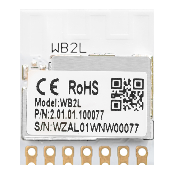
- Page 4 Contents WB2L is a low-power embedded Wi-Fi and BLE module that Tuya has developed. It consists of a highly integrated RF chip (BK7231T) and several peripheral com- ponents, with an embedded Wi-Fi network protocol stack and robust library func- tions.
-
Page 5: Product Overview
WB2L is embedded with a low-power 32-bit microcontroller unit (MCU), 2 MB flash memory, 256 KB static random-access memory (SRAM), and extensive peripher- als. WB2L is an RTOS platform that integrates all function libraries of the Wi-Fi MAC and TCP/IP protocols. You can develop embedded Wi-Fi products as required. 1.1 Features •... -
Page 6: Change History
2.1 Dimensions and footprint WB2L has one row of pins with a 2±0.1 mm pin spacing. The WB2L dimensions (Lx Wx H) are 17.3±0.35 mm x 15±0.35 mm x 2.8±0.15 mm. The following figure shows the WB2L front and rear views. - Page 7 2 MODULE INTERFACES 4 / 26...
-
Page 8: Interface Pin Definition
2 MODULE INTERFACES 2.2 Interface pin definition Pin No. Symbol I/O type Function PWM2 Hardware PWM pin , which is connected to the P8/BT_ACTIVE/PWM2 ( Pin24 ) PWM1 Hardware PWM pin , which is connected to the P7/WIFI_ACTIVE/PWM1 ( Pin23 ) 5 / 26... -
Page 9: Test Pin Definition
2 MODULE INTERFACES Pin No. Symbol I/O type Function PWM0 Hardware PWM pin , which is connected to the P6/CLK13M/PWM0 ( Pin22 ) PWM5 Hardware PWM pin, which is connected to the P26/IRDA/PWM5 ( Pin15 ) PWM4 Hardware PWM pin , which is connected to the P24/LPO_CLK/PWM4 (... - Page 10 2 MODULE INTERFACES Pin No. Symbol I/O type Function U2_TXD UART2_TX, LOG serial port U2_RXD UART2_RX, LOG serial port F_SCK Clock pin when data is downloaded from the flash memory, which is connected to the P20 pin on the internal IC F_CSN Command enabling pin...
-
Page 11: Electrical Parameters
3 ELECTRICAL PARAMETERS Pin No. Symbol I/O type Function F_SO Data output pin when data is downloaded from the flash memory, which is connected to the P23 pin on the internal IC 3 Electrical parameters 3.1 Absolute electrical parameters Minimum Maximum Parameter Description... -
Page 12: Working Conditions
3 ELECTRICAL PARAMETERS 3.2 Working conditions Minimum Typical Maximum Parameter Description value value value Unit Working ℃ tempera- ture VBAT Power supply voltage -0.3 VCC*0.25 low-level input VCC*0.75 high-level input VCC*0.1 low-level output VCC*0.8 high-level output Imax I/O drive current 3.3 Current consumption during constant transmission and receiving Working TX Power/... -
Page 13: Working Current
3 ELECTRICAL PARAMETERS Working TX Power/ Typical Maximum status Mode Rate Receiving value value Unit 11Mbps Constant receiving 54Mbps Constant receiving MCS7 Constant receiving 3.4 Working current Working Working status (Ta = Average Maximum mode 25°C) value value Unit The module is in EZ mode, and the Wi-Fi indicator... -
Page 14: Rf Features
4 RF FEATURES Working Working status (Ta = Average Maximum mode 25°C) value value Unit Disconnected The module is disconnected from the network, and the Wi-Fi indicator is steady off. 4 RF features 4.1 Basic RF features Parameter Description Frequency band 2.412~2.484GHz Wi-Fi standard IEEE 802.11b/g/n(channels1-14) -
Page 15: Rx Performance
4 RF FEATURES Minimum Maximum Parameter Value Typical Value Value Unit Average RF output power,802.11b CCK Mode Average RF 13.5 output power,802.11g OFDM Mode Average RF output power,802.11n OFDM Mode MCS7 EVM@802.11b CCK 11Mbps Mode 17dBm EVM@802.11g OFDM 54Mbps Mode 13.5dBm EVM@802.11n OFDM MCS7... - Page 16 4 RF FEATURES Minimum Maximum Parameter value Typical value value Unit PER<8%, RX sensitivity, 802.11b DSSS Mode PER<10%, RX sensitivity, 802.11g OFDM Mode PER<10%, RX sensitivity, 802.11n OFDM Mode MCS7 13 / 26...
-
Page 17: Antenna
5 ANTENNA 5 Antenna 5.1 Antenna type WB2L uses an onboard PCB antenna or Ipex antenna. 5.2 Antenna interference reduction To ensure optimal Wi-Fi performance when the Wi-Fi module uses an onboard PCB antenna, it is recommended that the antenna be at least 15mm away from other metal parts. - Page 18 5 ANTENNA 15 / 26...
- Page 19 5 ANTENNA 16 / 26...
-
Page 20: Packaging Information And Production Instructions
6 PACKAGING INFORMATION AND PRODUCTION INSTRUCTIONS 6 Packaging Information and Production Instructions 6.1 Mechanical Dimensions The PCB dimensions (L x Wx H) are 17.3±0.35mm (L)×15±0.35mm (W) ×2.8±0.15mm (H). 6.2 Side view 17 / 26... -
Page 21: Recommended Schematic Encapsulation
6 PACKAGING INFORMATION AND PRODUCTION INSTRUCTIONS 6.3 Recommended schematic encapsulation 6.4 Recommended PCB Encapsulation-Pin header WB2L can be mounted onto a PCB by using an SMT placement machine or through- hole mounted onto the PCB through a pin header. 18 / 26... -
Page 22: Recommended Pcb Encapsulation-Smt
6 PACKAGING INFORMATION AND PRODUCTION INSTRUCTIONS 6.5 Recommended PCB Encapsulation-SMT 19 / 26... -
Page 23: Production Instructions
1. Use an SMT placement machine to mount components to the stamp hole mod- ule that Tuya produces within 24 hours after the module is unpacked and the firmware is burned. If not, vacuum pack the module again. Bake the module before mounting components to the module. -
Page 24: Recommended Oven Temperature Curve
Electroless nickel immersion gold (ENIG) is used for the PCBs. If the solder pads are exposed to the air for over three months, they will be oxidized severely and dry joints or solder skips may occur. Tuya is not liable for such problems and consequences. - Page 25 6 PACKAGING INFORMATION AND PRODUCTION INSTRUCTIONS 22 / 26...
-
Page 26: Storage Conditions
6 PACKAGING INFORMATION AND PRODUCTION INSTRUCTIONS 6.8 Storage conditions 23 / 26... - Page 27 Packing each reel Reel Packs in MOQ ( pcs ) model method Pack Each Box WB2L 4000 Carrier tape 1000 and reel packing 8 Appendix: Statement FCC Caution: Any changes or modifications not expressly approved by the party responsible for compliance could void the user’s authority to operate this equip- ment.
- Page 28 This device have got an FCC ID: 2ANDL-WB3L. The final end product must be labeled in a visible area with the following: “Contains Transmitter Module FCC ID: 2ANDL- WB2L ” This device is intended only for OEM integrators under the following conditions: •...
- Page 29 8 APPENDIX: STATEMENT Hereby, Hangzhou Tuya Information Technology Co., Ltd declares that this module product is in compliance with essential requirements and other relevant provisions of Directive 2014/53/EU,2011/65/EU. A copy of the Declaration of conformity can be found at https://www.tuya.com This product must not be disposed of as normal household waste, in accordance with EU directive for waste electrical and electronic equipment (WEEE- 2012/19/EU).
Need help?
Do you have a question about the WB2L and is the answer not in the manual?
Questions and answers