Advertisement
Quick Links
UM2651
User manual
Discovery kit with STM32L4P5AG MCU
Introduction
®
The STM32L4P5G-DK Discovery kit is a complete demonstration and development platform for the STMicroelectronics Arm
®
Cortex
-M4 core-based STM32L4P5AGI6PU microcontroller with four I²C buses, three SPI and six USART ports, CAN port, two
SAI ports, 12-bit ADC, 12-bit DAC, internal 320-Kbyte SRAM and 1-Mbyte Flash memory, two Octo-SPI memory interfaces,
touch-sensing capability, USB OTG FS port, LCD-TFT controller, flexible memory controller (FMC), 8- to 14-bit DCMI interface
and JTAG debugging support.
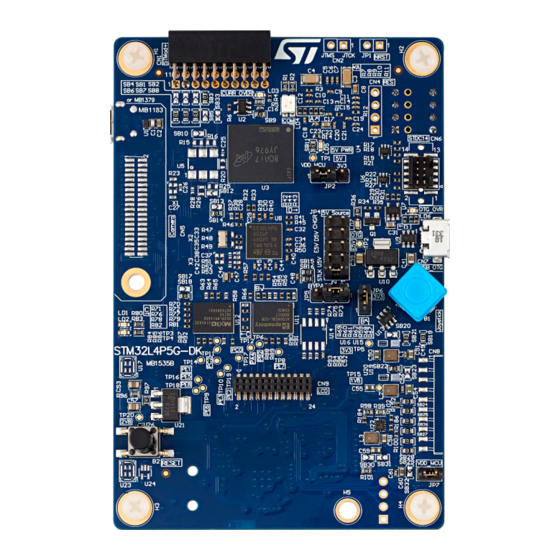
The STM32L4P5G-DK Discovery kit, shown in
Figure 1
and
Figure
2, is used as a reference design for user application
development before porting to the final product.
The full range of hardware features available on the board helps users improve application development evaluating all the
®
peripherals (USB OTG FS, Octo-SPI Flash and PSRAM memory device, eMMC, and others). ARDUINO
Uno V3 and STMod+
connectors provide easy connection to extension shields or daughterboards for specific applications.
An STLINK-V3E is integrated into the board, as the embedded in-circuit debugger and programmer for the STM32 MCU and the
USB Virtual COM port bridge.
Figure 1.
STM32L4P5G-DK top view
Figure 2.
STM32L4P5G-DK bottom view
Pictures are not contractual.
UM2651 - Rev 2 - September 2020
www.st.com
For further information contact your local STMicroelectronics sales office.
Advertisement

Related Manuals for ST STM32L4P5AG

Summary of Contents for ST STM32L4P5AG
- Page 1 UM2651 User manual Discovery kit with STM32L4P5AG MCU Introduction ® The STM32L4P5G-DK Discovery kit is a complete demonstration and development platform for the STMicroelectronics Arm ® Cortex -M4 core-based STM32L4P5AGI6PU microcontroller with four I²C buses, three SPI and six USART ports, CAN port, two...
- Page 2 4-Gbyte onboard eMMC • On-board current measurement • SAI audio codec (Footprint only) • ST-MEMS digital microphone (Footprint only) • 512-Mbit Octo-SPI NOR Flash memory with DDR mode • 64-Mbit Octo-SPI PSRAM memory with DDR mode • 2 user LEDs •...
- Page 3 UM2651 Ordering information Ordering information To order the STM32L4P5G-DK Discovery kit, refer to Table 1. Additional information is available from the datasheet and reference manual of the target STM32. Table 1. Ordering information Order code Board reference Target STM32 STM32L4P5G-DK MB1535 STM32L4P5AGI6PU Codification...
- Page 4 STM32 Flash memory for easy demonstration of the device peripherals in standalone mode. The latest versions of the demonstration source code and associated documentation can be downloaded from www.st.com. UM2651 - Rev 2 page 4/37...
- Page 5 UM2651 Conventions Conventions Table 3 provides the conventions used for the ON and OFF settings in the present document. Table 3. ON/OFF convention Convention Definition Jumper JPx ON Jumper fitted Jumper JPx OFF Jumper not fitted Jumper JPx [1-2] Jumper fitted between Pin 1 and Pin 2 Solder bridge SBx ON SBx connections closed by 0 Ω...
- Page 6 UM2651 Delivery recommendations Delivery recommendations Before first use, check the board for any damage that might have occurred during shipment, that all socketed components are firmly fixed in their sockets and that none are loose in the plastic bag. UM2651 - Rev 2 page 6/37...
- Page 7 UM2651 Hardware layout and configuration Hardware layout and configuration The STM32L4P5G-DK Discovery kit is designed around the STM32L4P5AGI6PU target microcontroller. Figure 3 illustrates STM32L4P5AGI6PU connections with peripheral components. Figure 4 shows the location of the main components on the top side of the Discovery board and Figure 5 shows the location of the main components on the bottom side of the Discovery board.
- Page 8 UM2651 Hardware layout and configuration Figure 4. STM32L4P5G-DK PCB layout (Top view) SWCLK and SWDIO STMod+ connector STLINK-V3E STLINK-V3E COM overcurrent alarm ST-LINK SWD 5V PWR STDC14 connector Camera connector USB-OTG overcurrent USB-OTG STM32L4P5AGI6PU USB-OTG connector 5V source selection LD1, LD2...
- Page 9 UM2651 Hardware layout and configuration Figure 5. STM32L4P5G-DK PCB layout (Bottom view) CN11 STLINK-V3E STLINK-V3E switcher CN12, CN14 ARDUINO ® connector ARDUINO ® CN13, CN15 ® ARDUINO connector CN16 CN17 Audio OUT MFX SWD UM2651 - Rev 2 page 9/37...
- Page 10 UM2651 Hardware layout and configuration Figure 6 provides the mechanical dimensions of the STM32L4P5G-DK board. Figure 6. STM32L4P5G-DK board mechanical dimensions (Top view) UM2651 - Rev 2 page 10/37...
- Page 11 The STLINK-V3E requires drivers to be installed on Windows . It embeds a firmware that needs to be updated in order to benefit from new functionalities or corrections. Refer for details to the technical note Overview of ST-LINK derivatives TN1235.
- Page 12 UM2651 Power supply If a short-circuit occurs on the board, the STMPS2151 power switch protects the USB port of the host PC against a current demand exceeding 500 mA. In such an event, the LD3 LED lights up. The STM32L4P5G-DK board can also be supplied from a USB power source not supporting enumeration, such as a USB charger.
- Page 13 UM2651 Clock references Jumper /solder Setting Configuration bridge Default setting. R46 ON R46 V is connected to VDD_MCU. connection is not connected to VDD_MCU. R46 OFF Default setting. VDDA and VDDUSB terminal of STM32L4P5AGI6PU are connected to VDD_MCU. JP2 VDDA / VDDUSB connection VDDA and VDDUSB terminal of STM32L4P5AGI6PU are...
- Page 14 The I²C-bus addresses of CS42L51-CNZ are 0x95 and 0x94. Digital microphones (Footprint only) Two ST-MEMS IMP34DT05TR digital microphones, U17 and U23, are available on STM32L4P5G-DK. The two microphones are located at a distance of 21 mm from each other. They are connected to the STM32 DFSDM by the PE9 port, generating the clock, and by PD3 port, collecting the PDM interleaved data.
- Page 15 UM2651 MFX MCU 6.13 MFX MCU The MFX MCU is used as an MFX multi-function expander and an IDD measurement calculator. 6.13.1 The MFX circuit on the STM32L4P5G-DK Discovery kit acts as IO-expander. The communication interface between MFX and STM32L4P5AGI6PU is the I2C1 bus. The signals connected to MFX are listed in Table Table 6.
- Page 16 UM2651 LCD interface (Connector only) 6.14 LCD interface (Connector only) The STM32L4P5G-DK supports 6 bits RGB interface and a touch-panel interface. The users may develop their daughterboard, plugged into the CN9 connector, for application. The CN9 connector part number is SAMTEC FLE-112-01-G-DV.
- Page 17 Ecosystem of microcontrollers. By default, it is designed to support an ST-dedicated fanout board to connect different modules or board extensions from different manufacturers. The fanout board also embeds a 3.3 V regulator and I C level shifter (Footprint only).
- Page 18 UM2651 CN5 camera module connector (Footprint only) CN5 camera module connector (Footprint only) Figure 8. CN5 camera module connector (Top view) Table 9. CN5 camera module connector pinout Pin number Description Pin number Description DCMI_D10 (PI3) DCMI_D11 (PH15) DCMI_D8 (PH6) DCMI_D9 (PH7) I2C4_SCL (PF14) I2C4_SDA (PF15)
- Page 19 UM2651 CN6 STDC14 connector CN6 STDC14 connector Figure 9. CN6 STDC14 debugging connector (Top view) Table 10. CN6 STDC14 debugging connector pinout Terminal Function / MCU port Terminal Function / MCU port SWDIO/TMS (PA13) SWDCLK/TCK (PA14) SWO/TDO (PB3) RESET# VCP_RX_STDC (PA3) VCP_TX_STDC (PA2) CN7 USB OTG FS Micro-AB connector A USB OTG Full Speed communication link is available at CN7 USB Micro-AB receptacle connector.
- Page 20 UM2651 CN11 STLINK-V3E USB Micro-B connector Pin number Description Pin number Description CN11 STLINK-V3E USB Micro-B connector The CN11 USB connector is used to connect the onboard STLINK-V3E facility to the PC for flashing and debugging software. Figure 11. CN11 Micro-B connector (Top view) Table 12.
- Page 21 UM2651 CN12, CN13, CN14, and CN15 ARDUINO® Uno V3 connectors ® CN12, CN13, CN14, and CN15 ARDUINO Uno V3 connectors ® CN12, CN13, CN14, and CN15 ARDUINO Uno V3 connectors are female connectors compatible with ® ® ARDUINO Uno Revision 3 standard. Most of the shields designed for ARDUINO Uno V3 fit the STM32L4P5G- DK board.
- Page 22 UM2651 CN16 audio green jack - line out (Footprint only) CN16 audio green jack - line out (Footprint only) A 3.5 mm stereo audio green jack output CN16 is available on the STM32L4P5G-DK board to support headphones. Figure 12. CN16 stereo headset with a microphone jack Table 14.
- Page 23 UM2651 CN9 LCD connector 7.10 CN9 LCD connector Figure 13. CN9 LCD connector Table 15. CN9 LCD connector Terminal Terminal name MCU port Terminal Terminal name MCU port LCD_DE LCD_R7 LCD_DISP LCD_R6 LCD_HSYNC LCD_G7 LCD_VSYNC LCD_G6 LCD_CLK LCD_B7 LCD_B6 TP_INT TP_RST LCD_PWM_EN PA15...
- Page 24 UM2651 STM32L4P5G-DK I/O assignment STM32L4P5G-DK I/O assignment Table 16. STM32L4P5G-DK I/O assignment UFBGA169 + Pin name Type Input level STM32 pinout assignment ext SMPS PI10 JOY_RIGHT SMPS_V1 DCMI_D2/D2 FT_fa TP_RST FT_la JTDO/TRACESWO PA15 LCD_PWM_EN PA14 JTCK/SWCLK PA13 JTMS/SWDIO ARD_SPI2_NSS_TIM5_CH4 PH14 DCMI_D4/D4 JOY_DOWN DCMI_D7/D7...
- Page 25 UM2651 STM32L4P5G-DK I/O assignment UFBGA169 + Pin name Type Input level STM32 pinout assignment ext SMPS JOY_UP SAI1_FS_A FT_l LCD_R6 FT_l LCD_R7 FT_fl SDMMC1_D5 FT_fla I2C1_SDA PG10 FT_s OCTOSPIM_P2_IO7 OCTOSPIM_P1_IO5 SDMMC1_CMD PC10 SDMMC1_D2 DCMI_D5/D5 DCMI_D0/D0 FT_f SMPS_PG || DCMI_D9/D9 PA12 FT_u OTG_FS_DP PC13...
- Page 26 UM2651 STM32L4P5G-DK I/O assignment UFBGA169 + Pin name Type Input level STM32 pinout assignment ext SMPS VDDIO2 PC15-OSC32_OUT OSC32_OUT OCTOSPIM_P2_IO3 OCTOSPIM_P2_CLK MFX_WAKEUP PG14 FT_fs LED2 PG13 FT_fs LED1 FT_f SAI1_SCK_A FT_fl SDMMC1_D1 SDMMC1_D0 FT_s OCTOSPIM_P1_DQS SDMMC1_D7 PH0-OSC_IN OSC_IN NRST NRST PF10 STMOD_DFSDM1_CKOUT FT_a...
- Page 27 UM2651 STM32L4P5G-DK I/O assignment UFBGA169 + Pin name Type Input level STM32 pinout assignment ext SMPS PD10 STMOD_INT FT_a OCTOSPIM_P1_IO6 VSSA/VREF- FT_a MFX_IRQ_OUT TT_a ARD_STMOD_ADC12_IN10 TT_la ARD_ADC12_IN15 PF15 FT_f I2C4_SDA LCD_B7 PE14 STMOD_SPI1_MISO2 FT_f SMPS_V2 PD14 ARD_TIM4_CH3 PD12 FT_fl STMOD_USART3_RTS_DE PD11 STMOD_USART3_CTS_NSS PD13...
- Page 28 UM2651 STM32L4P5G-DK I/O assignment UFBGA169 + Pin name Type Input level STM32 pinout assignment ext SMPS FT_la USART2_TX FT_la ARD_ADC12_IN6 OPAMP2_VINM FT_a LCD_RTC_OUT2 PF12 OCTOSPIM_P2_DQS PE11 OCTOSPIM_P1_NCS PB10 FT_fl ARD_USART3_TX FT_f DCMI_HSYNC/DE PB12 STMOD_DFSDM1_DATIN1 PB13 FT_fl ARD_SPI2_SCK UM2651 - Rev 2 page 28/37...
- Page 29 Evaluation tools marked as “ES” or “E” are not yet qualified and therefore not ready to be used as reference design or in production. Any consequences deriving from such usage will not be at ST charge. In no event, ST will be liable for any customer usage of these engineering sample tools as reference designs or in production.
- Page 30 UM2651 Federal Communications Commission (FCC) and ISED Canada Compliance Statements Appendix A Federal Communications Commission (FCC) and ISED Canada Compliance Statements FCC Compliance Statement Part 15.19 This device complies with Part 15 of the FCC Rules. Operation is subject to the following two conditions: (1) this device may not cause harmful interference, and (2) this device must accept any interference received, including interference that may cause undesired operation.
- Page 31 UM2651 ISED Compliance Statement Étiquette de conformité à la NMB-003 d'ISDE Canada : CAN ICES-3 (B) / NMB-3 (B). UM2651 - Rev 2 page 31/37...
- Page 32 UM2651 Revision history Table 17. Document revision history Date Revision Changes 19-Dec-2019 Initial release Updated: • Section 6.14 LCD interface (Connector only) Added: • Section 7.10 CN9 LCD connector 18-Sep-2020 • Section 9 STM32L4P5G-DK information with moved updated Product marking Section 9.2 Board revision history •...
- Page 33 UM2651 Contents Contents Features................2 Ordering information .
- Page 34 UM2651 Contents 6.13.1 MFX ..............15 6.13.2 IDD measurement .
- Page 35 UM2651 List of tables List of tables Table 1. Ordering information..............3 Table 2.
- Page 36 UM2651 List of figures List of figures Figure 1. STM32L4P5G-DK top view ............1 Figure 2.
- Page 37 ST’s terms and conditions of sale in place at the time of order acknowledgement. Purchasers are solely responsible for the choice, selection, and use of ST products and ST assumes no liability for application assistance or the design of Purchasers’...
Need help?
Do you have a question about the STM32L4P5AG and is the answer not in the manual?
Questions and answers