HOLT ADK-2130mPCIe Technical Manual
Hide thumbs
Also See for ADK-2130mPCIe:
- Quick start manual (17 pages) ,
- Technical manual (69 pages) ,
- Quick start manual (22 pages)
Advertisement
Quick Links
Advertisement

Related Manuals for HOLT ADK-2130mPCIe


Summary of Contents for HOLT ADK-2130mPCIe
- Page 1 ADK-2130mPCIe Technical Manual Jan. 16, 2020 AN-2130mPCIe_New 01/20...
- Page 2 This page intentionally blank...
- Page 3 REVISION HISTORY Revision Date Description of Change AN-2130mPCIe 1/16/20 Initial Release Rev. New Holt Integrated Circuits...
- Page 4 This Technical Manual covers the hardware, software and instructions for how to transfer the Holt Flash Drive (FD) files to the user’s PC. See the Quick Start Guide (QSG) for an introduction to the card, Application Development Kit (ADK) contents and how to run the demonstration software using the Holt bootable Flash Drive.
- Page 5 PC requirements Linux OS: Ubuntu: 16.04.6 LTS or 18.04 LTS (Holt FD installed). System RAM: 8G is recommended for Eclipse, 16G for Vivado. Hard Drive Capacity: 10G minimum for the Eclipse project. Mini PCIe Slot Standard Full size F2 USB 2.0 or 3.0 Port: For transferring Holt Flash Drive files.
-
Page 6: Break Out Board
8 is a list of the signals and descriptions on the inter-connect ribbon J4 connector. For board component locations, connectors, IC’s and test points, see Figure 3 – Board References at the end of the document. Two break-out boards are available. Single channel: mPCIe_breakout-1F Dual channel: mPCIe_breakout-2F – mPCIe_breakout-2F break-out board Figure 2 Holt Integrated Circuits... -
Page 7: First Things First
4. The Ubuntu OS on the Holt FD cannot be used to install Ubuntu on a user’s PC. If the user has an older version of Ubuntu than 18.04 LTS it may be possible to upgrade it. - Page 8 “Make Link” to create a link. Drag the link to the desktop. The Holt demo software is comprised of three project sub-folders residing in a single Eclipse workspace folder. On the Ubuntu OS home folder create a Holt folder.
- Page 9 The three project folder should be shown in the PE. 5. Project descriptions for the three project are contained in sub-folders: Holt Integrated Circuits...
- Page 10 Demo – The Demo software resets both devices and initializes both devices using the Holt API library functions. There are two build configurations: Debug and Debug_precompiled_library. The Debug_precompiled_library requires a binary library file produced by the H1553Libary project. See below. Rebuilding the ‘Debug’ configuration compiles all the demo files including the Holt API library files and outputs the Demo executable.
- Page 11 10. Clean and Rebuild the Demo project. There are two Demo project targets: “debug” rebuilds the Holt API source files and Demo files to produce the Demo executable. This is the easiest and fastest way to rebuild the Demo project. Without Holt API source files the Debug_precompiled_library target must be used.
- Page 12 11. There are two ways to run the Demo (after loading the kernel module and rebuilding the Demo project). The first method is to simply open a terminal window in the Holt directory and execute the ‘run’ bash script. This will load the kernel module and execute the Demo program automatically.
- Page 13 Holt Integrated Circuits...
- Page 14 The BC is initialized to transmit messages and the RT and SMT are initialized to be able to read and write 1553 data words. The Holt HI-613x API manual should be studied along with the Demo code to gain a better overall understand how the code works before making modifications.
- Page 15 Demos Execute the Demo program by executing the ‘run’ script in the Holt folder. The QSG provides instructions how to execute the ‘run’ script and run most of the demos. The run script contains eight terminal commands. cd PcieDual2130Eclipse/pcie_kernel_module sudo sh holt_pcie_unload sudo sh holt_pcie_load cd ..
- Page 16 There is no menu command to disable an internal RT once it’s been enabled but the card and program can be reset by using command ‘4’ to start similar to the state when the Demo program is first launched. >n > Holt Integrated Circuits...
- Page 17 2525 2626 2727 2828 2929 3030 3131 3232 Dev0 MSG #0006. TIME = 00044814us BUS A TYPE0: BC to RT CMD1 1BC0 --> 03-R-30-00 DATA 0101 0202 0303 0404 0505 0606 0707 0808 0909 1010 1111 1212 1313 1414 1515 1616 Holt Integrated Circuits...
- Page 18 CMD1 1BC0 --> 03-R-30-00 DATA 0101 0202 0303 0404 0505 0606 0707 0808 0909 1010 1111 1212 1313 1414 1515 1616 1717 1818 1919 2020 2121 2222 2323 2424 2525 2626 2727 2828 2929 3030 3131 3232 STA1 1800 Holt Integrated Circuits...
- Page 19 CMD1 182A --> 03-R-01-10 CMD2 0C2A --> 01-T-01-10 STA1 0800 DATA BBBB 0202 1414 0404 0505 0606 0707 0808 0909 1010 STA2 1800 HoltBCSendAsyncMsgHP returns 0 > Dev0 MSG #1533. TIME = 00042566us BUS B TYPE0: BC to RT Holt Integrated Circuits...
- Page 20 BUS A TYPE0: BC to RT CMD1 1822 --> 03-R-01-02 DATA 0005 0002 STA1 1800 Dev0 MSG #0287. TIME = 00099356us BUS A TYPE2: RT to RT CMD1 182A --> 03-R-01-10 CMD2 0C2A --> 01-T-01-10 STA1 0800 Holt Integrated Circuits...
- Page 21 P_NTRUM = 1 P_RT1ENA = 1 P_RT2ENA = 1 P_INHIBIT = 0 P_INPUTCONTROL demo/user mode= 0 0=demo, 1=user P_SPAREINPUT = 0 P_MTPKTRDY = 1 P_ACTIVE = 0 P_RT1MC8 = 1 P_RT2MC8 = 1 P_READY = 1 > Holt Integrated Circuits...
-
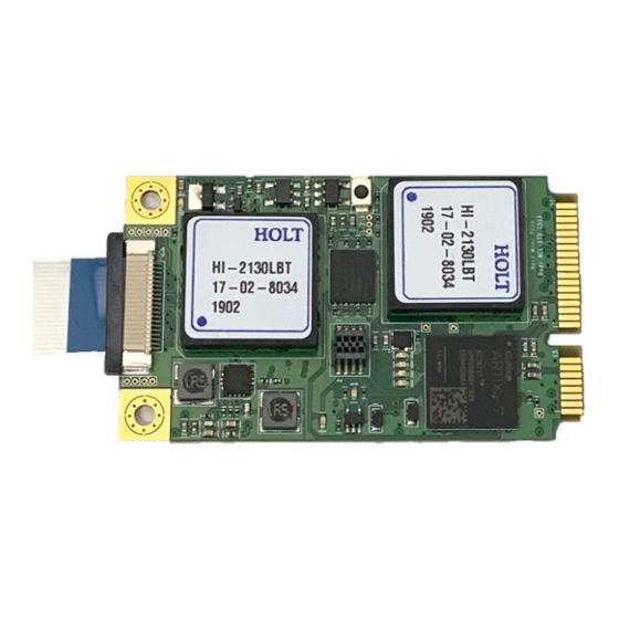
Page 22: Hardware Description
Hardware Description The Holt Mini PCIe card features two Holt HI-2130 dual-redundant multi-terminals on a 50.95mm x 30mm form factor per the PCI Express Mini Card Electromechanical Specification. A Xilinx XC7A12T FPGA serves as the interface between two HI-2130s and the PCIe Gen2 bus. The host communicates with the card using the built-in PCIe drivers in the Linux OS once a PCIe link is established after power up. - Page 23 0x8011 Read only Optional read RT2MC8 Device->FPGA RT2 Mode Code 8 0x8012 Read only Optional read Indicates Ready Optional read. Used by READY Device->FPGA 0x8013 Read only state demo software to determine when devices are ready after Holt Integrated Circuits...
- Page 24 FPGA initialization sequence is complete and asserts the DONE_0 signal high. LED D10 lights up when the FPGA is in a configuration reset state and will turn off when the initialization is complete. Xilinx provides a complete technical guide on the FPGA configuration sequence. See Xilinx UG470. Holt Integrated Circuits...
- Page 25 COMMENTS CONNECTOR Address pins: [A15:A0] Address bus Data bus pins: [D15:D0] Bidirectional data bus Read strobe (Intel mode) Write strobe (Intel mode) MCLK50 Master 50MHz input clock from FPGA MTTCLK Optional clock, TBD TTCLK Optional clock, TBD Holt Integrated Circuits...
- Page 26 MTRUN0 Input, controlled by FPGA. READY0, ACTIVE0 Outputs, Inputs to FPGA. Function TBD. MTPKTRDY0 Output, Not used or TBD. TXINHA,TXINHB Both inhibit inputs connected to CH0INHIBIT0 on connector. Default is enabled. Assert low to disable both Transmitters. Holt Integrated Circuits...
- Page 27 Both inhibit inputs connected to CH1INHIBIT1 TXINHA,TXINHB on the connector. Default is enabled. Assert high to disable both Transmitters. J4 connector input pins: Transmit Inhibit, BCENAx, BCTRIG are ESD protected but the DC steady state voltage should not exceed 3.6V. Holt Integrated Circuits...
-
Page 28: Power Supply
VCCO3V3 1000mA 200mA Flash, Osc and Misc. 3.3V 3V3aux 2 x HI-2130 1600mA 1553 messaging duty cycle dependant (PCIe conn.) 1.5V (PCIe MGTAVCC1V Provides clean 150mA <100mA conn.) power to the GBT MGTAVCTT1V2 150mA <100mA (PCIe bus) Holt Integrated Circuits... - Page 29 0 & 1 1.86 50 with fan 45 with fan 0 & 1 1.78 0 & 1 1.02 .655 0 & 1 0 & 1 IDLE Note: ICC will be less with typical 75Ω bus coupler impedance. Holt Integrated Circuits...
- Page 30 Channel 0 BC Trigger. 10K pull-up. SPARE INPUT Unused. CH1INHBIT1 Channel 0 Transmit Inhibit. 10K pull-up. Inverted direct connect to 2130 inhibit pins. CH1 BCENAB Channel 1 BC Enable. 10K pull-up. CH1 BCTRIG Channel 1 BC Trigger. 10K pull-up. Logic GND Holt Integrated Circuits...
-
Page 31: System Clocks
An ADC input is provided on a test point but this feature is not implemented in the current design. The user has the option to implement this if there is a requirement. FPGA Spare Pins See the schematic for spare pins. Holt Integrated Circuits... - Page 32 Figure 3 – Board References Holt Integrated Circuits...
- Page 33 Summary This technical guide summarized the steps necessary to install the Holt Mini PCIe Eclipse project and import the project into Eclipse to allow building the projects and rerunning them. See technical guide AN-MPCIeVivado Technical Guide for information on the Xilinx FPGA design.
- Page 34 Holt Integrated Circuits, Inc. Bill of Materials PCB P/N: HV047 EV-2130mPCIe-1F Rev.A Evaluation Board Item Qty Description Reference Digikey P/N Mfg P/N PCB, Bare, Evaluation Board 399-8939-1-ND Kemet C0402C100C8GACTU Cap Cer 10pF 10V COG/NPO 0402 SMD C5,C9 Cap Cer 0.01uF 16V X7R 0402 SMD...
- Page 35 Holt Integrated Circuits, Inc. Bill of Materials PCB P/N: HV047 EV-2130mPCIe-1F Rev.A Evaluation Board 1497-1219-1-ND SunLED XZVG68W-2 Green Led, Clear 0402 SMD D1,D2,D6,D7,D8,D9,D10 Conn 8-Pin 0.8mm Micro Socket CLE-104-01-G-DV Samtec CLE-104-01-G-DV Through Hole 3-Pin Connector J3 (DNI) None None SAM14910CT-ND Samtec ZF5S-20-01-T-WT-TR Conn Zero Insertion 20-pos,0.5mm FFC...
- Page 36 Holt Inc. Bill of Materials PCB P/N: HV051 mPCIe_breakout-1F Rev.B Item Description Reference DigiKey Mfr P/N 1 PCB, Bare, Eval Board -------- NewTek # 13989 1 Conn FFC Bottom 5mm R/A SAM14910CT-ND Samtec ZF5S-20-01-T-WT-TR 1 Cable FFC 20 Pos 0.5mm 5" Long...
- Page 37 Holt Integrated Circuits, Inc. Bill of Materials PCB P/N: HV047 EV-2130mPCIe-2F Rev.A Evaluation Board Item Qty Description Reference Digikey P/N Mfg P/N PCB, Bare, Evaluation Board 399-8939-1-ND Kemet C0402C100C8GACTU Cap Cer 10pF 10V COG/NPO 0402 SMD C5,C9 Cap Cer 0.01uF 16V X7R 0402 SMD...
- Page 38 Holt Integrated Circuits, Inc. Bill of Materials PCB P/N: HV047 EV-2130mPCIe-2F Rev.A Evaluation Board 1497-1219-1-ND SunLED XZVG68W-2 Green Led, Clear 0402 SMD D1,D2,D6,D7,D8,D9,D10 Conn 8-Pin 0.8mm Micro Socket CLE-104-01-G-DV Samtec CLE-104-01-G-DV Through Hole 3-Pin Connector J3 (DNI) None None SAM14910CT-ND Samtec ZF5S-20-01-T-WT-TR Conn Zero Insertion 20-pos,0.5mm FFC...
- Page 39 Holt Inc. Bill of Materials PCB P/N: HV051 mPCIe_breakout-2F Rev.B Item Description Reference DigiKey Mfr P/N 1 PCB, Bare, Eval Board -------- NewTek # 13989 1 Conn FFC Bottom 5mm R/A SAM14910CT-ND Samtec ZF5S-20-01-T-WT-TR 1 Cable FFC 20 Pos 0.5mm 5" Long...
- Page 40 LD39015 SOT23-5L Title Title Title Note 1: Holt PCIe-Mini dual MIL-STD 1553 Holt PCIe-Mini dual MIL-STD 1553 Holt PCIe-Mini dual MIL-STD 1553 Distribute power over planes to where they need to go under the Size Size...
- Page 41 IO_L13N_T2_MRCC_15 JTAG IO_L14P_T2_SRCC_15 IO_L14N_T2_SRCC_15 IO_L19N_T3_A21_VREF_15 0.47uF 0.47uF BANK 15 Title Title Title Holt PCIe-Mini dual MIL-STD 1553 Holt PCIe-Mini dual MIL-STD 1553 Holt PCIe-Mini dual MIL-STD 1553 XC7A12T-2CPG238 Size Size Size Document Number Document Number Document Number R e v...
- Page 42 MGTAVTT1V2 3V3aux 3V3aux .1uF .1uF .1uF CHANNEL 0 Title Title Title Holt PCIe-Mini dual MIL-STD 1553 Holt PCIe-Mini dual MIL-STD 1553 Holt PCIe-Mini dual MIL-STD 1553 Size Size Size Document Number Document Number Document Number R e v R e v R e v <Doc>...
- Page 43 MGTAVTT1V2 3V3aux 3V3aux .1uF .1uF .1uF CHANNEL 1 Title Title Title Holt PCIe-Mini dual MIL-STD 1553 Holt PCIe-Mini dual MIL-STD 1553 Holt PCIe-Mini dual MIL-STD 1553 Size Size Size Document Number Document Number Document Number R e v R e v R e v <Doc>...
- Page 44 3V3aux 3V3aux led3 READY0 DEV012 READY1 DEV112 Title Title Title ACTIVE0 DEV013 ACTIVE1 DEV113 Holt PCIe-Mini dual MIL-STD 1553 Holt PCIe-Mini dual MIL-STD 1553 Holt PCIe-Mini dual MIL-STD 1553 nIRQ0 DEV014 nIRQ1 DEV114 nMR0 DEV015 nMR1 DEV115 Size Size Size...
Need help?
Do you have a question about the ADK-2130mPCIe and is the answer not in the manual?
Questions and answers