
Related Manuals for Epson S5U13A05P00C100


Summary of Contents for Epson S5U13A05P00C100
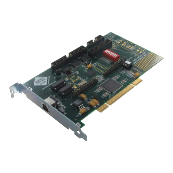
- Page 1 S1D13A05 LCD/USB Companion Chip S5U13A05P00C100 Evaluation Board User Manual Document Number: X40A-G-014-01.02 Rev. 1.02...
- Page 2 This evaluation board/kit or development tool is intended for use by an electronics engineer and is not a consumer product. The user should use it properly and in a safe manner. Seiko Epson does not assume any responsibility or liability of any kind of damage and/or fire caused by the use of it.
-
Page 3: Table Of Contents
11 Sales and Technical Support ......30 Seiko Epson Corporation S5U13A05P00C100 Evaluation Board Rev. 1.02... - Page 4 Seiko Epson Corporation S5U13A05P00C100 Evaluation Board Rev. 1.02...
-
Page 5: Introduction
Introduction 1 Introduction This manual describes the setup and operation of the S5U13A05P00C100 Evaluation Board. The board is designed as an evaluation platform for the S1D13A05 LCD/USB Companion Chip. This document is updated as appropriate. Please check for the latest revision of this document before beginning any development. -
Page 6: Features
• Direct interface for 18-bit TFT Type 2 LCD panel support • Direct interface for 18-bit TFT Type 3 LCD panel support • Direct interface for 18-bit TFT Type 4 (Epson ND-TFD) LCD panel support. • Connector for USB client support. -
Page 7: Installation And Configuration
Installation and Configuration 3 Installation and Configuration The S5U13A05P00C100 is designed to support as many platforms as possible. The S5U13A05P00C100 incorporates a DIP switch and three jumpers which allow both the evaluation board and the S1D13A05 LCD controller to be configured for a specified evalu- ation platform. - Page 8 CLKI to BCLK Divide ratio 2:1 CLKI to BCLK divide ratio 1:1 SW1-8 Disable PCI bridge for non-PCI host Enable PCI bridge for PCI host = Required settings when using the PCI Bridge FPGA Seiko Epson Corporation S5U13A05P00C100 Evaluation Board Rev. 1.02...
-
Page 9: Configuration Jumpers
Installation and Configuration 3.2 Configuration Jumpers The S5U13A05P00C100 has three jumper blocks which configure various settings on the board. The jumper positions for each function are shown below. Table 3-2: Jumper Summary Jumper Function Position 1-2 Position 2-3 No Jumper LCD Panel Voltage +3.3V LCDVCC... - Page 10 When the jumper is at position 2-3, the GPO0 signal is inverted and then sent (active low) to H3. When no jumper is installed, GPO0 is not sent to H3. GPIO0 not Inverted Normal sent to H1 (Active Low) (Active High) Figure 3-4: Configuration Jumper (JP5) Location Seiko Epson Corporation S5U13A05P00C100 Evaluation Board Rev. 1.02...
-
Page 11: Cpu Interface
If the target MC68K bus is 32-bit, then these signals should be connected to D[31:16]. These pins are not used in their corresponding host interface mode. Systems are responsible for externally connecting them to IO V Seiko Epson Corporation S5U13A05P00C100 Evaluation Board Rev. 1.02... -
Page 12: Cpu Bus Connector Pin Mapping
Connected to WE0# of the S1D13A05 Connected to WAIT# of the S1D13A05 Connected to CS# of the S1D13A05 Connected to MR# of the S1D13A05 Connected to WE1# of the S1D13A05 Connected to +3.3V Seiko Epson Corporation S5U13A05P00C100 Evaluation Board Rev. 1.02... - Page 13 +5 volt supply +5 volt supply Connected to RD/WR# of the S1D13A05 Connected to BS# of the S1D13A05 Connected to BUSCLK of the S1D13A05 Connected to RD# of the S1D13A05 Not connected Not connected Seiko Epson Corporation S5U13A05P00C100 Evaluation Board Rev. 1.02...
-
Page 14: Lcd Interface Pin Mapping
FPSHIFT. For further FPDATxx to LCD interface mapping, see S1D13A05 Hardware Functional Specification, document number X40A-A-001-xx. GPO0 can be inverted on H1 by setting JP5 to 2-3. Seiko Epson Corporation S5U13A05P00C100 Evaluation Board Rev. 1.02... - Page 15 GPO1 VCOM GPO1 GPO2 XOEV GPO2 GPO3 GPO3 GPO4 PCLK1 GPO4 GPO5 PCLK2 GPO5 GPO6 XRESH GPO6 GPO7 XRESV GPO7 GPO8 XOHV GPO8 GPO9 XSTBY GPO9 GPO10 PMDE GPO10 2-26 Even Numbers Seiko Epson Corporation S5U13A05P00C100 Evaluation Board Rev. 1.02...
-
Page 16: Technical Description
PCI Bridge FPGA to support the PCI bus. 6.2 Direct Host Bus Interface Support The S5U13A05P00C100 is specifically designed to work using the PCI Bridge FPGA in a standard PCI bus environment. However, the S1D13A05 directly supports many other host bus interfaces. -
Page 17: Lcd Panel Support
Section 5, “LCD Interface Pin Mapping” on page 14. S5U13A05P00C100 does not provide a power supply for the LCD bias voltage needed by Passive LCD panels. An external power supply is required to provide the bias LCD voltage to the LCD panel. -
Page 18: Tft Type 3 Extended Lcd Connector
The S1D13A05 supports interrupts using the output pin, IRQ. In order to support interrupts from the USB client of the S1D13A05, the S5U13A05P00C100 evaluation board connects IRQ to PCI interrupt INTA# from the PCI slot. The IRQ pin output to the PCI bus can be disabled by removing jumper JP4. -
Page 19: Parts List
Do not populate. 1M 0805 0805 Resistor, 1M, 1% 470R 0805 0805 Resistor, 470R, 1% R30,R31,R36 1K 5% 1206 Resistor, 1K, 5% 100K 5% 1206 Resistor, 100K, 5% 1.5K 1% 1206 Resistor, 1.5K, 1% Seiko Epson Corporation S5U13A05P00C100 Evaluation Board Rev. 1.02... - Page 20 Screw, pan head, #4-40 x 1/4” Resistor SMD 0805 0ohm 0805 Resistor, 0 ohm Epson SG8002DB, 50MHz, (U6) 50MHz Oscillator DIP14, 50MHz socketed Epson SG8002DB, 6.5MHz, (U7) 6.5MHz Oscillator DIP14, 6.5MHz socketed Seiko Epson Corporation S5U13A05P00C100 Evaluation Board Rev. 1.02...
-
Page 21: Schematics
Schematics 8 Schematics Figure 8-1: S1D13A05P00C100 Schematics (1 of 6) Seiko Epson Corporation S5U13A05P00C100 Evaluation Board Rev. 1.02... - Page 22 Schematics Figure 8-2: S1D13A05P00C100 Schematics (2 of 6) Seiko Epson Corporation S5U13A05P00C100 Evaluation Board Rev. 1.02...
- Page 23 Schematics Figure 8-3: S1D13A05P00C100 Schematics (3 of 6) Seiko Epson Corporation S5U13A05P00C100 Evaluation Board Rev. 1.02...
- Page 24 Schematics Figure 8-4: S1D13A05P00C100 Schematics (4 of 6) Seiko Epson Corporation S5U13A05P00C100 Evaluation Board Rev. 1.02...
- Page 25 Schematics Figure 8-5: S1D13A05P00C100 Schematics (5 of 6) Seiko Epson Corporation S5U13A05P00C100 Evaluation Board Rev. 1.02...
- Page 26 Schematics Figure 8-6: S1D13A05P00C100 Schematics (6 of 6) Seiko Epson Corporation S5U13A05P00C100 Evaluation Board Rev. 1.02...
-
Page 27: Board Layout
Board Layout 9 Board Layout Figure 9-1: S5U13A05P00C100 Board Layout (Top View) Seiko Epson Corporation S5U13A05P00C100 Evaluation Board Rev. 1.02... - Page 28 Board Layout Figure 9-2: S5U13A05P00C100 Board Layout (Bottom View) Seiko Epson Corporation S5U13A05P00C100 Evaluation Board Rev. 1.02...
-
Page 29: Change Record
• released as Rev 1.0 X40A-G-014-00 Revision 0.01 - Issued: October 4, 2006 • created from S5U13A05B00C User Manual, X40A-G-004-xx • added updated parts list • added updated schematics • minor edits Seiko Epson Corporation S5U13A05P00C100 Evaluation Board Rev. 1.02... -
Page 30: Sales And Technical Support
Sales and Technical Support 11 Sales and Technical Support For more information on Epson Display Controllers, visit the Epson Global website. https://global.epson.com/products_and_drivers/semicon/products/display_controllers/ For Sales and Technical Support, contact the Epson representative for your region. https://global.epson.com/products_and_drivers/semicon/information/support.html Seiko Epson Corporation S5U13A05P00C100 Evaluation Board...
Need help?
Do you have a question about the S5U13A05P00C100 and is the answer not in the manual?
Questions and answers