Sony XDP-PK1000 Service Manual
Digital link sound system
Hide thumbs
Also See for XDP-PK1000:
- Operating instructions manual (52 pages) ,
- Specification sheet (3 pages) ,
- Installation/connections (2 pages)
Table of Contents
Advertisement
SERVICE MANUAL
Ver. 1.0 2011.07
Photo: XA-C100IP
• XDP-PK1000 are composed of following models.
DSP master unit
Cradle
Amplifi er
Subwoofer
Note: Please refer to service manual separately issued for XM-PK100D
and XS-PK120LC.
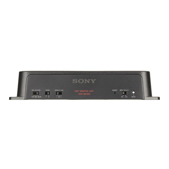
DSP Master Unit (XDP-MU100)
AUDIO POWER SPECIFICATIONS
CEA2006 Standard
Power Output: 17 Watts RMS 4 at
4 Ohms < 1% THD+N
SN Ratio: 80 dBA
(reference: 1 Watt into 4 Ohms)
Power-AMP
Output: Speaker outputs 4 CH
(Front L/R, Rear L/R)
Speaker impedance: 4 Ω – 8 Ω
Maximum power output: 45 W × 4 (at 4 Ω)
iPhone®, iPod®, iPod classic®,
iPod nano®, and iPod touch® are
trademarks of Apple Inc., registered in the
U.S. and other countries.
9-893-244-01
Sony Corporation
2011G33-1
©
2011.07
Published by Sony Techno Create Corporation
XDP-PK1000
XDP-MU100
XA-C100IP
XM-PK100D
XS-PK120LC
SPECIFICATIONS
General
Outputs:
Audio output terminals: (Front/Rear)
Subwoofer output terminal (mono)
Power amplifier control terminal
Inputs:
iPod signal input terminal (dock connector)
Hi-level input terminal
Sound controls:
Bass/Treble ±7 dB
Fader/Balance ±7 steps
SUB-W Volume +/- 6Step , No sound
Power requirements: 12 V DC car battery
(negative ground (earth))
Dimensions: (Mounting dimensions)
Approx. 210.6 mm × 40 mm × 156.6 mm
3
5
1
(8
/
in × 1
/
in × 6
/
in) (w/h/d)
8
8
4
Mass: Approx. 0.92 kg (2 lb 1 oz)
Supplied accessories:
Card remote commander: RM-X251
Parts for installation and connections (1set)
XDP-PK1000
XA-C100IP/XDP-MU100
Photo: XDP-MU100
Cradle (XA-C100IP)
Dimensions:
Approx. 65 mm × 138.8* mm × 105.3 mm
5
1
1
(2
/
in × 5
/
in × 4
/
in) (w/h/d)
8
2
4
Mass: Approx. 0.14 kg (5 oz)
7
* Arm fully extended: 147.1 mm (5
/
8
Design and specifications are subject to change
without notice.
NOTES ON CHIP COMPONENT REPLACEMENT
•
Never reuse a disconnected chip component.
•
Notice that the minus side of a tantalum capacitor may be dam-
aged by heat.
DIGITAL LINK SOUND SYSTEM
US Model
in
) (h)
Advertisement
Table of Contents

Related Manuals for Sony XDP-PK1000


Summary of Contents for Sony XDP-PK1000
- Page 1 XDP-PK1000 XA-C100IP/XDP-MU100 SERVICE MANUAL US Model Ver. 1.0 2011.07 Photo: XA-C100IP Photo: XDP-MU100 • XDP-PK1000 are composed of following models. XDP-PK1000 DSP master unit XDP-MU100 Cradle XA-C100IP Amplifi er XM-PK100D Subwoofer XS-PK120LC Note: Please refer to service manual separately issued for XM-PK100D and XS-PK120LC.
-
Page 2: Table Of Contents
XDP-PK1000 SECTION 1 SERVICING NOTES TABLE OF CONTENTS UNLEADED SOLDER Boards requiring use of unleaded solder are printed with the lead- free mark (LF) indicating the solder contains no lead. SERVICING NOTES ..........(Caution: Some printed circuit boards may not come printed with... -
Page 3: General
óptimo. Before Installation Nota Póngase en contacto con su distribuidor Sony más cercano en caso de tener cualquier consulta o problema relativos al Install the DSP master unit under the front passenger Antes de la instalación sistema que no se hayan tratado en este manual. - Page 4 Striped Rayado Rayado unit. In this case, please consult your nearest Sony unidad maestra del DSP. En tal caso, póngase en Car audio unit dealer. contacto con su distribuidor Sony más cercano.
- Page 5 XDP-PK1000 Before Installation Installation To remove the cradle Arranging the cradle Note on the suction cup of the cradle Press the ridges to remove the cradle cable cable ount the cradle on the dashboard where it Mount the clip of the strap on the from the cradle.
-
Page 6: Disassembly
XDP-PK1000 SECTION 3 DISASSEMBLY • This set can be disassembled in the order shown below. 3-1. DISASSEMBLY FLOW XDP-MU100 3-2. BRACKET (BOTTOM) (Page 6) 3-3. DSP BOARD BLOCK (Page 7) 3-4. DSP BOARD (Page 7) Note: Follow the disassembly procedure in the numerical order given. -
Page 7: Dsp Board Block
XDP-PK1000 3-3. DSP BOARD BLOCK 2 screw (P2.6 3 two screws 1 two screws (P2.6 (+B P-TITE M2) 6 DSP board block 5 two claws Note: Please spread a sheet under a unit not to injure front panel. – Bottom side view –... -
Page 8: Test Mode
XDP-PK1000 SECTION 4 TEST MODE 4. SOUND TEST VIA SWITCH Note: Test mode of XDP-MU100 has been described in this sec- Fader, SubVolume, Balance can be changed by EQ setting switch tion. Test mode doesn’t exist in XA-C100IP. in test mode (Refer to table for details). - Page 9 3. Touch the screen of iPod/iPhone in the following order. 1.0.0 1.0.0 1.0.0 1.0.0 iPod/iPhone Controller “Settings” t “General” t “About” t “XDP-PK1000” software version 4. Software version is displayed. Confi rm software version is the following. System Controller software version (IC202) : 0.0.00 iPod/iPhone Controller software version (IC703) : 1.0.0...
-
Page 10: Diagrams
XDP-PK1000 SECTION 5 DIAGRAMS 5-1. BLOCK DIAGRAM - AUDIO INPUT Section (XDP-MU100) - iPod/iPhone CONTROLLER CN301 (1/2) IC703 CRADLE DIGITAL SIGNAL CONVERTER IC605 DEC_DATA 90 BSIF_DATA PIO15/SDO0 SDIN_O D– D– DEC_BCK 91 BSIF_BCK (Page 11) PIO18/LRCK0 LRCLK_O DEC_BCKIN VBUS-USB USB_VBUS... -
Page 11: Block Diagram - Audio Output Section (Xdp-Mu100)
XDP-PK1000 5-2. BLOCK DIAGRAM - AUDIO OUTPUT Section (XDP-MU100) - ELECTRICAL VOLUME DIGITAL SIGNAL PROCESSOR IC410 IC409 J402 SDIN_O 25 SDIN3 AUXL1 56 33 IN_FL OUT_FL 36 FRONT (Page 10) LRCLK_O 26 LRCLK0 AUXR1 57 R-CH AUDIO OUT BCK_O 27 BCLK0... -
Page 12: Block Diagram - Panel, Power Supply Section (Xdp-Mu100)
XDP-PK1000 5-3. BLOCK DIAGRAM - PANEL, POWER SUPPLY Section (XDP-MU100) - SYSTEM CONTROLLER IC202 (3/3) RESET (Page 10) XOUT RESET X202 +3.3V SIGNAL 32.768kHz RESET 12 CDON_CHECK REGULATOR (Page 10) GENERATOR IC203 IC201 OSCOUT X201 BU +3.3V REGULATOR 7.92MHz IC102 (2/2) - Page 13 XDP-PK1000 THIS NOTE IS COMMON FOR PRINTED WIRING BOARDS AND SCHEMATIC DIAGRAMS. • Waveforms (In addition to this, the necessary note is printed in each block.) – DSP Board – For Printed Wiring Boards. For Schematic Diagrams. IC202 qa (XOUT)
-
Page 14: Printed Wiring Board - Dsp Board (Component Side) (Xdp-Mu100)
XDP-PK1000 5-4. PRINTED WIRING BOARD - DSP Board (Component Side) (XDP-MU100) - • : Uses unleaded solder. DSP BOARD (COMPONENT SIDE) D111 Q406 C482 R115 C106 R458 D112 Q405 Q404 Q403 Q401 R116 C757 C753 C756 C751 C754 C750 R467... -
Page 15: Printed Wiring Board - Dsp Board (Conductor Side) (Xdp-Mu100)
XDP-PK1000 5-5. PRINTED WIRING BOARD - DSP Board (Conductor Side) (XDP-MU100) - • : Uses unleaded solder. DSP BOARD (CONDUCTOR SIDE) J402 (FRONT VIEW) AUDIO OUT REAR FRONT CN101 CN301 CN402 REAR LCH (+) CRADLE HIGH LEVEL FRONT LCH (+) -
Page 16: Schematic Diagram - Dsp Board (1/3) (Xdp-Mu100)
XDP-PK1000 5-6. SCHEMATIC DIAGRAM - DSP Board (1/3) (XDP-MU100) - • See page 13 for waveforms. • See page 19 for IC Block Diagrams. • See page 23 for IC Pin Function Description. DSP BOARD (1/3) JL114 R121 Q101-103 BATTERY CHECK... -
Page 17: Schematic Diagram - Dsp Board (2/3) (Xdp-Mu100)
XDP-PK1000 5-7. SCHEMATIC DIAGRAM - DSP Board (2/3) (XDP-MU100) - • See page 13 for waveforms. • See page 19 for IC Block Diagrams. DSP BOARD (2/3) R431 FRONT IC B/D AUDIO OUT JL409 JL410 IC102 R432 REAR R433 J402... -
Page 18: Schematic Diagram - Dsp Board (3/3) (Xdp-Mu100)
XDP-PK1000 5-8. SCHEMATIC DIAGRAM - DSP Board (3/3) (XDP-MU100) - • See page 13 for waveforms. • See page 19 for IC Block Diagrams. • See page 23 for IC Pin Function Description. DSP BOARD (3/3) L304 R738 R723 R743... - Page 19 XDP-PK1000 • IC Block Diagrams – DSP Board – IC102 TDF8556AJ/N5 I2C_SIO OUT-FL– C BUS I2C_SCK OUT-FL+ OUT-RL– P-GND1 OUT-RL+ IN-RL IN-FL S-GND PROTECTION/ DIAGNOSTIC IN-FR IN-RR BEEP OUT-RR+ P-GND3 OUT-RR– OUT-FR+ STANDBY/ MUTE OUT-FR– CHIP DETECT/ P-GND4 DIAGNOSTIC TEMPERATURE...
- Page 20 XDP-PK1000 IC302 BD9070FP-E2 PVIN PVIN N.C. – N.C. VREGB 1 – – VIN 2 LOGIC – N.C. 3 SLOPE N.C. 4 PGND 5 UVLO, TSD, SOFT GND 6 OVP, OCP, SCP START – RT 7 SYNC VREF EN 8 VREG...
- Page 21 XDP-PK1000 IC409 ADW10005Z-1 76 75 74 73 72 71 70 69 68 67 66 65 64 63 62 61 FILTA VREF AGND AVDDD1 VOUT3 59 VOUT2 58 VOUT1 57 AUXR1 SYNC DELAY 56 AUXL1 MEMORY 55 AVDD3 54 HPOUTR 53 HPOUTL...
- Page 22 XDP-PK1000 IC410 BD3467FV-E2 FADER FADER BOOST OUTC FADER FADER A1 1 BOOST OUTS A2 2 FADER FADER B1 3 OUTR1 BOOST B2 4 FADER FADER OUTR2 BOOST CP1 5 FADER FADER CN 6 OUTF1 BOOST CP2 7 FADER FADER OUTF2...
- Page 23 XDP-PK1000 • IC Pin Function Description DSP BOARD IC202 R5F3650KBDFA (SYSTEM CONTROLLER) Pin No. Pin Name Description 1, 2 Not used SIRCS SIRCS signal input from the CRADLE connector 4 to 7 Not used BYTE External data bus width selection signal input terminal Fixed at “L”...
- Page 24 XDP-PK1000 Pin No. Pin Name Description 76 to 78 Not used USB_ON USB power on/off control signal output to the DC/DC converter “H”: power on USB_OVER USB over current detection signal input terminal “L”: over current RE-IN1 Jog dial pulse signal input from the CRADLE connector (B phase input)
- Page 25 XDP-PK1000 DSP BOARD IC605 TC94A99FG-003 (SY) (DIGITAL SIGNAL CONVERTER) Pin No. Pin Name Description LPFO Signal output for PLL loop fi lter to the operation amplifi er Not used PVREF Reference voltage (+1.65V) input terminal Not used VCOF VCO fi lter terminal...
- Page 26 XDP-PK1000 Pin No. Pin Name Description DAO4 (R_L-CH) Rear L-channel data output terminal Not used DVDD5 Power supply terminal (+3.3V) DAO5 (SUB-CH) Sub channel data output terminal Not used DVSS5 Ground terminal VDD1-3 Power supply terminal (+1.5V) VSS-2 Ground terminal...
- Page 27 XDP-PK1000 DSP BOARD IC703 92FD28AFG7F88 (SYJZ) (iPod/iPhone CONTROLLER) Pin No. Pin Name Description System reset signal input from the reset signal generator, system controller and RESET switch RESET “L”: reset For several hundreds msec. after the power supply rises, “L” is input, then it change to “H”...
- Page 28 XDP-PK1000 Pin No. Pin Name Description VBUS_ON VBUS power on/off control signal output to the system controller “H”: power on Two-way USB data (positive) with the CRADLE connector D− Two-way USB data (negative) with the CRADLE connector CPU operation mode setting signal input terminal Fixed at “H”...
-
Page 29: Exploded View
XDP-PK1000 SECTION 6 EXPLODED VIEW Note: • -XX and -X mean standardized parts, so • The mechanical parts with no reference they may have some difference from the number in the exploded views are not sup- original one. plied. • Items marked “*” are not stocked since •... -
Page 30: Electrical Parts List
XDP-PK1000 SECTION 7 ELECTRICAL PARTS LIST Note: • Due to standardization, replacements in • RESISTORS • SEMICONDUCTORS the parts list may be different from the All resistors are in ohms. In each case, u: μ, for example: parts specifi ed in the diagrams or the com- METAL: Metal-fi... - Page 31 XDP-PK1000 Ref. No. Part No. Description Remark Ref. No. Part No. Description Remark C432 1-165-908-11 CERAMIC CHIP 1uF C495 1-116-401-91 CERAMIC CHIP 0.1uF C433 1-165-908-11 CERAMIC CHIP 1uF C496 1-100-567-81 CERAMIC CHIP 0.01uF C434 1-165-908-11 CERAMIC CHIP 1uF C497 1-100-597-91 CERAMIC CHIP 0.1uF...
- Page 32 XDP-PK1000 Ref. No. Part No. Description Remark Ref. No. Part No. Description Remark D102 8-719-083-66 DIODE UDZSUSTE-1718B IC603 6-714-504-01 IC MM3404A15URE D103 6-502-961-01 DIODE DA2J10100L IC605 6-715-712-01 IC TC94A99FG-003 (SY) D104 6-501-571-01 DIODE 1N5404-C311-3 IC702 6-713-560-01 IC MFI341S2162 D105 6-502-961-01...
- Page 33 XDP-PK1000 Ref. No. Part No. Description Remark Ref. No. Part No. Description Remark R118 1-216-833-11 METAL CHIP 1/10W R286 1-216-821-11 METAL CHIP 1/10W R119 1-218-965-11 METAL CHIP 1/16W R287 1-216-821-11 METAL CHIP 1/10W R120 1-216-295-91 SHORT CHIP R288 1-218-977-11 METAL CHIP...
- Page 34 XDP-PK1000 Ref. No. Part No. Description Remark Ref. No. Part No. Description Remark R413 1-208-688-11 METAL CHIP 1.6K 0.5% 1/16W R603 1-216-295-91 SHORT CHIP R414 1-208-688-11 METAL CHIP 1.6K 0.5% 1/16W R604 1-216-295-91 SHORT CHIP R415 1-208-688-11 METAL CHIP 1.6K 0.5%...
- Page 35 XDP-PK1000 Ref. No. Part No. Description Remark Ref. No. Part No. Description Remark R738 1-218-941-81 METAL CHIP 1/16W PARTS FOR INSTALLATION AND CONNECTIONS R739 1-218-965-11 METAL CHIP 1/16W (for DSP master unit) R740 1-218-965-11 METAL CHIP 1/16W ************************************** R742 1-218-967-11...
- Page 36 XDP-PK1000 REVISION HISTORY Checking the version allows you to jump to the revised page. Also, clicking the version at the top of the revised page allows you to jump to the next revised page. Ver. Date Description of Revision 2011.07...
Need help?
Do you have a question about the XDP-PK1000 and is the answer not in the manual?
Questions and answers