Wiznet WizFi360 Hardware Design Manual
Hide thumbs
Also See for WizFi360:
- At instruction set (68 pages) ,
- User manual (50 pages) ,
- Firmware update manual (16 pages)

Related Manuals for Wiznet WizFi360


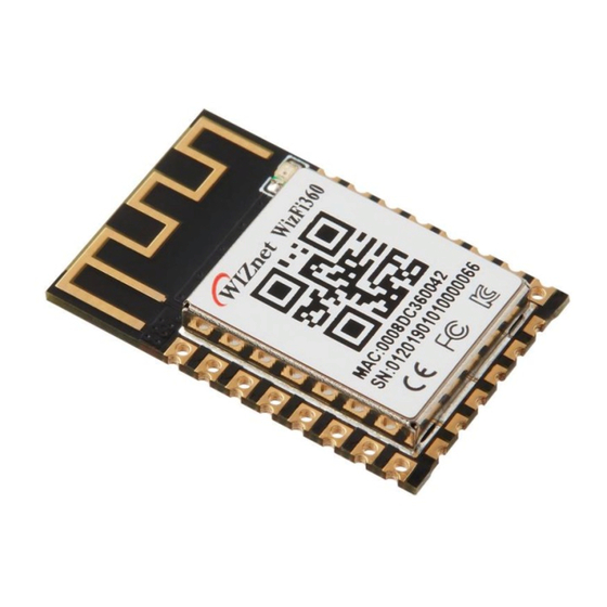
Summary of Contents for Wiznet WizFi360
- Page 1 WizFi360 Hardware Design Guide (Version 1.02) http://www.wiznet.io © Copyright 2019 WIZnet Co., Ltd. All rights reserved.
- Page 2 Document Revision History Date Revision Changes 2019-09-02 Initial Release Edited “Figure 5. UART Level Shifter” 2019-09-03 1.01 Added “4. PCB Footprint” 2019-09-20 1.02 Edited “Figure 2. Reference Schematic” 2 / 13 WizFi360 Hardware Design Guide...
-
Page 3: Table Of Contents
Initial Value of GPIO Pins ........................5 2.1. Circuit ..................................6 System................................6 3.1. 3.2. Power ................................7 3.3. UART ................................7 3.4. ETC .................................. 8 PCB Footprint ..............................10 PCB layout ................................11 3 / 13 WizFi360 Hardware Design Guide... -
Page 4: Overview
1. Overview This document is the WizFi360 hardware design guide. If you are designing hardware using the WizFi360 you must refer to this document. This document includes a reference circuit diagram and a PCB guide. 2. Pin Definitions TXD1 I2C_SDA... -
Page 5: Initial Value Of Gpio Pins
*Note: UART1 is used for AT command and data communication. UART0 is used for debugging and firmware upgrade. 2.1. Initial Value of GPIO Pins This is the initial value of GPIO when using AT command to use GPIO on the WizFi360. Pin Name Type... -
Page 6: Circuit
3. Circuit 3.1. System The WizFi360 has a very simple circuit. You can connect power to the WizFi360 and send and receive data through UART1. And you have to pay attention to the four pins. Figure 2. Reference Schematic ⚫... -
Page 7: Power
WP circuit offers to design user configuration. You must control this pin if you are using standby mode. If this pin is high in Standby mode, the WizFi360 is reset to the normal operating mode. 3.2. Power WizFi360 requires the use of a power supply capable of supplying 3.0V to 3.6V and more than 500mA. -
Page 8: Etc
The UART voltage on the WizFi360 is 3.3V. However, your MCU may not have a voltage of 3.3V. If so you need a Level Shifter to connect the WizFi360 to your MCU. You can design a Level Shifter circuit by referring to Figure 4. Connect your MCU’s UART voltage to the VCCIO at Figure 4. - Page 9 Figure 5. UART Level Shifter 9 / 13 WizFi360 Hardware Design Guide...
-
Page 10: Pcb Footprint
4. PCB Footprint Figure 6. Recommended PCB Land Pattern of WizFi360 10 / 13 WizFi360 Hardware Design Guide... -
Page 11: Pcb Layout
5. PCB layout Power wiring width should not be less than 30mil. ⚫ Except for the antenna portion of WizFi360, the bottom layer of the shield can must have ⚫ a GND plane. Figure 7. GND Figures. 6 and Figures. 7 are 2 antenna placement which can best performance of ⚫... - Page 12 Figure 8. Best Placement 1 Figure 9. Best Placement 2 12 / 13 WizFi360 Hardware Design Guide...
- Page 13 Copyright Notice Copyright 2019 WIZnet Co., Ltd. All Rights Reserved. Technical Support: https://forum.wiznet.io/ Sales & Distribution: sales@wiznet.io For more information, visit our website at http://www.wiznet.io/ 13 / 13 WizFi360 Hardware Design Guide...
Need help?
Do you have a question about the WizFi360 and is the answer not in the manual?
Questions and answers