Table of Contents
Advertisement
Quick Links
The MB90910 series, loaded 1 channel FULL-CAN controller and Flash ROM, is general-purpose Cypress 16-bit microcontroller
designing for automotive and industrial applications. Its main feature is the on-board CAN controllers, which conform to Ver 2.0 Part
A and Part B, while supporting a very flexible message buffer scheme and so offering more functions than a normal FULL-CAN
approach. With the new 0.18
The power supply (1.8 V) is supplied to the MCU core from an internal regulator circuit. This creates a major advantage in terms of
EMI and power consumption.
The internal PLL clock frequency multiplier provides an internal 31.25 ns instruction execution time from an external 4 MHz clock.
The unit features a 4-channel input capture unit 1 channel 16-bit free-run timer, 2-channel LIN-UART,
1-channel UART, and 16-channel 8/10-bit A/D converter as the peripheral resource.
Features
Clock
Built-in PLL clock frequency multiplication circuit
■
Selection of machine clocks (PLL clocks) is allowed among
■
frequency division by 2 on oscillation clock and multiplication
of 1 to 8 times of oscillation clock (for 4 MHz oscillation clock,
4 MHz to 32 MHz)
Minimum execution time of instruction : 31.25 ns (when
■
operating with 4-MHz oscillation clock and 8-time multiplied
PLL clock)
Instruction system best suited to controller
16 Mbytes CPU memory space
■
24-bit internal addressing
■
Wide choice of data types (bit, byte, word, and long word)
■
Wide choice of addressing modes (23 types)
■
Enhanced multiply-divide instructions with sign and RETI
■
instructions
Enhanced high-precision computing with 32-bit accumulator
■
Instruction system compatible with high-level
language (C language) and multitask
Employing system stack pointer
■
Enhanced various pointer indirect instructions
■
Barrel shift instructions
■
Increased processing speed
4-byte instruction queue
Powerful interrupt function
Powerful 8-level, 34-condition interrupt feature
■
Up to 8 channels external interrupts are supported
■
CPU-independent automatic data transfer func-
tion
Expanded intelligent I/O service function (EI
channels
Cypress Semiconductor Corporation
Document Number: 002-04578 Rev. *A
m CMOS technology, Cypress now offers on-chip Flash ROM program memory up to 128 Kbytes.
2
OS) : up to 16
•
198 Champion Court
MB90911AS/F912BS/V950AMAS
2
F
MC-16LX MB90910 Series
16-bit Microcontroller
Low power consumption (standby) mode
Sleep mode (a mode that halts CPU operating clock)
■
Main timer mode (timebase timer mode that is transferred
■
from main clock mode)
PLL timer mode (timebase timer mode that is transferred from
■
PLL clock mode)
Stop mode (a mode that stops oscillation clock)
■
CPU blocking operation mode
■
Process
CMOS technology
I/O port
General purpose input/output port (CMOS output) :
- 36 ports
Timer
Timebase timer, watchdog timer : 1 channel
■
8/16-bit PPG timer : 8-bit
■
16-bit reload timer : 2 channels
■
16- bit input/output timer
■
-16-bit free-run timer : 1 channel (FRT0 : ICU 0/1/2/3)
❐
-16- bit input capture : (ICU) : 4 channels
❐
FULL-CAN controller : 1 channel
Compliant with CAN specifications Version 2.0 Part A and B
■
16 message buffers are built in
■
CAN wake-up function
■
UART (LIN/SCI) : LIN-UART2 channels, UART
1 channel
Equipped with full-duplex double buffer
■
Clock-asynchronous or clock-synchronous serial trans-
■
mission is available
,
•
San Jose
CA 95134-1709
6 channels or 16-bit
3 channels
•
408-943-2600
Revised April 12, 2016
Advertisement
Table of Contents

Subscribe to Our Youtube Channel
Related Manuals for Cypress MB90910 Series


Summary of Contents for Cypress MB90910 Series
- Page 1 MC-16LX MB90910 Series 16-bit Microcontroller The MB90910 series, loaded 1 channel FULL-CAN controller and Flash ROM, is general-purpose Cypress 16-bit microcontroller designing for automotive and industrial applications. Its main feature is the on-board CAN controllers, which conform to Ver 2.0 Part A and Part B, while supporting a very flexible message buffer scheme and so offering more functions than a normal FULL-CAN ...
- Page 2 MB90910 Series DTP/External interrupt : up to 8 channels, CAN Program patch function wakeup : up to 1 channel Address matching detection for 6 address pointers Module for activation of expanded intelligent I/O service (EI Capable of changing input voltage for port...
-
Page 3: Table Of Contents
MB90910 Series Contents Product Lineup ..............4 AC Characteristics ............. 43 Pin Assignment ..............6 Clock Timing .............. 43 Pin Description ..............7 Reset Standby Input ..........45 I/O Circuit Type .............. 10 Power-on Reset ............46 Handling Devices ............15 UART ................. -
Page 4: Product Lineup
MB90910 Series 1. Product Lineup Part number MB90V950AMAS MB90F912BS MB90911AS Parameter Type Evaluation product Flash memory product MASK ROM product MC-16LX CPU On-chip PLL clock multiplier ( 8, 1/2 when PLL stops) System clock ... - Page 5 MB90910 Series (Continued) Part number MB90V950AMAS MB90F912BS MB90911AS Parameter 8 channels 4 channels 16-bit Rising edge, falling edge or rising & falling edge sensitive Input capture Signals an interrupt upon external event 8 channels (16-bit) /16 channels (8-bit) 3 channels (16-bit) /6 channels (8-bit)
-
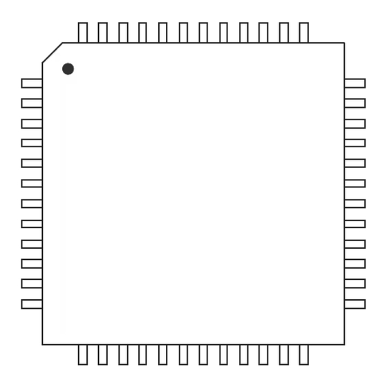
Page 6: Pin Assignment
MB90910 Series 2. Pin Assignment MB90F912BS, MB90911AS ■ (TOP VIEW) P20* AVcc P21/PPGB(A)* P60/AN0 P22/PPGD(C)* P61/AN1 P23/PPGF(E)* P62/AN2 P24/IN0 P63/AN3 P25/IN1 LQFP-48 P64/AN4 P26/IN2 P65/AN5/PPGA(B) P27/IN3 P66/AN6/PPGC(D) P67/AN7/PPGE(F) P80/ADTG/INT12R P50/AN8/SIN2 (FPT-48P-M26) * : High current output port Document Number: 002-04578 Rev. *A... -
Page 7: Pin Description
MB90910 Series 3. Pin Description Pin No. Pin name I/O circuit type* Function power input pin for analog circuit. Power (Vref) input pin for A/D converter. It should be below V P60 to P64 General-purpose I/O port. 3 to 7 AN0 to AN4 Analog input pins for A/D converter. - Page 8 MB90910 Series I/O circuit Pin No. Pin name Function type* General-purpose I/O port (Different I/O circuit type from MB90V950AMAS). AN14 Analog input pin for A/D converter. INT11 External interrupt request input pin for INT11. General-purpose I/O port (Different I/O circuit type from MB90V950AMAS).
- Page 9 MB90910 Series (Continued) I/O circuit Pin No. Pin name Function type* General-purpose I/O port. TX output pin for CAN1 controller. General-purpose I/O port. RX input pin for CAN1 controller. INT9R External interrupt request input pin for INT9R. General-purpose I/O port.
-
Page 10: I/O Circuit Type
MB90910 Series 4. I/O Circuit Type Type Circuit Remarks Oscillation circuit : High-speed oscillation feedback resistor approx. 1 M Xout (MASK ROM product, Flash memory product) Standby control signal Oscillation circuit : High-speed oscillation feedback resistor approx. 1 M... - Page 11 MB90910 Series Type Circuit Remarks CMOS hysteresis input pin Pull-up resistor CMOS hysteresis inputs (Continued) Document Number: 002-04578 Rev. *A Page 11 of 64...
- Page 12 MB90910 Series Type Circuit Remarks • CMOS level output 4 mA, I 4 mA) P-ch • CMOS hysteresis inputs 0.8Vcc V 0.2Vcc) Pout (With the standby-time input shutdown func- tion) N-ch • Automotive input (With the Nout...
- Page 13 MB90910 Series Type Circuit Remarks Protection circuit for power supply input P-ch N-ch • CMOS level output 20 mA, I 14 mA) 4 mA, I 4 mA) (MB90V950: I Pull-up control Pull-up • CMOS hysteresis inputs resistor 0.8Vcc V...
- Page 14 MB90910 Series (Continued) Type Circuit Remarks • CMOS level output = 4 mA) = 4 mA, I P-ch Pout • CMOS hysteresis inputs 0.8Vcc V 0.2Vcc) (With the standby-time input shutdown func- N-ch tion) Nout • Automotive input (With the standby-time input shutdown func-...
-
Page 15: Handling Devices
On this microcontroller, if in case the crystal oscillator breaks off or an external reference clock input stops while the PLL clock mode is selected, a self-oscillator circuit contained in the PLL may continue its operation at its self-running frequency. However, Cypress will not guarantee results of operations if such failure occurs. - Page 16 MB90910 Series Pull-up/down resistors The MB90910 series does not support internal pull-up/down resistors (Port 2 : built-in pull-up resistors) . Use external components ■ where needed. Crystal oscillator circuit Noises around X0 or X1 pin may be possible causes of malfunctions. Make sure to provide bypass capacitors via shortest distance from X0, X1 pins, crystal oscillator (or ceramic resonator) and ground lines, and make sure, that lines of oscillation circuit do not cross the lines of other circuits.
- Page 17 If DIRECT bit is set to ’0’ (initial value) , wait states will be performed when accessing CAN registers. Note : Please refer to Hardware Manual of “MB90910 series for detail of CAN Direct Mode Register”. 14. Flash security function The security bit is located in the area of the Flash memory.
-
Page 18: Block Diagrams
MB90910 Series 6. Block Diagrams MB90V950AMAS ■ X0, X1 Clock MC-16LX controller core 16-bit FRCK0 I/O timer 0 Input IN7 to IN0 capture 8 channels Output 30 Kbytes OUT7 to OUT0 compare 8 channels Prescaler 16-bit (7 channels) free-run FRCK1... - Page 19 MB90910 Series MB90F912BS, MB90911AS ■ Clock X0, X1 MC-16LX controller core Input capture IN0 to IN3 4 channels 16-bit FRCK0 I/O timer 0 Flash* controller 1 channel -bit TIN2, TIN3 Prescaler reload 3 channels timer TOT2, TOT3 2 channels SOT0, SOT1, SOT2...
-
Page 20: Memory Map
MB90910 Series 7. Memory Map MB90F912BS MB90911AS MB90V950AMAS FFFFFF FFFFFF FFFFFF ROM (FF bank) ROM (FF bank) ROM (FF bank) FF0000 FF0000 FF0000 FEFFFF FEFFFF ROM (FE bank) ROM (FE bank) FE0000 FE0000 FDFFFF ROM (FD bank) FD0000 FCFFFF ROM (FC bank) -
Page 21: I/O Map
MB90910 Series 8. I/O Map Abbrevia- Address Register Access Resource name Initial value tion 000000 Reserved 0001 000002 Port 2 Data Register PDR2 Port 2 XXXXXXXX 000003 Reserved 000004 Port 4 Data Register PDR4 Port 4 XXXXXXXX 000005 Port 5 Data Register... - Page 22 MB90910 Series Abbrevia- Address Register Access Resource name Initial value tion 000020 Serial Mode Register 0 SMR0 W, R/W 000000000 000021 Serial Control Register 0 SCR0 W, R/W 00000000 00000000 000022 Reception/Transmission Data Register 0 RDR0/TDR0 111111111 000023 Serial Status Register 0...
- Page 23 MB90910 Series Abbrevia- Address Register Access Resource name Initial value tion PPG E Operation Mode Control 00004C PPGCE W, R/W 01000111 Register PPG F Operation Mode Control 00004D PPGCF W, R/W 16-bit PPG E/F 01000001 Register PPG E/PPG F Count Clock Select...
- Page 24 MB90910 Series Abbrevia- Address Register Access Resource name Initial value tion Delayed Interrupt 00009F Delayed Interrupt/Release Register DIRR Generation 11111110 module Low-Power Low-power Consumption Mode 0000A0 LPMCR W, R/W Consumption 00011000 Control Register Control Circuit Low-Power 0000A1 Clock Selection Register...
- Page 25 MB90910 Series Abbrevia- Address Register Access Resource name Initial value tion 0000C1 Reserved 0000C2 Reserved 0000C3 Reserved 0000C9 0000CA External Interrupt Enable 1 ENIR1 00000000 0000CB External Interrupt Source 1 EIRR1 XXXXXXXX DTP/External 0000CC 00000000 Interrupt Detection Level Setting 1...
- Page 26 MB90910 Series Abbrevia- Address Register Access Resource name Initial value tion 00791C Reload Register LE PRLLE XXXXXXXX 00791D Reload Register HE PRLHE XXXXXXXX 16-bit PPG E/F 00791E Reload Register LF PRLLF XXXXXXXX 00791F Reload Register HF PRLHF XXXXXXXX 007920 Input Capture Register 0...
- Page 27 MB90910 Series Abbrevia- Address Register Access Resource name Initial value tion 0079A2 Flash Write Control Register 0 FWR0 00000000 Flash 0079A3 Flash Write Control Register 1 FWR1 00000000 0079A4 Reserved 0079B1 0079B2 Reserved 0079B3 Reserved 0079B7 0079B8 Reserved 0079B9 Reserved...
- Page 28 MB90910 Series (Continued) Abbrevia- Address Register Access Resource name Initial value tion 0079F0 Detect Address Setting Register 3 PADR3 XXXXXXXX 0079F1 Detect Address Setting Register 3 PADR3 XXXXXXXX 0079F2 Detect Address Setting Register 3 PADR3 XXXXXXXX 0079F3 Detect Address Setting Register 4...
-
Page 29: Can Controllers
MB90910 Series 9. CAN Controllers Conforms to CAN Specification Ver 2.0 Part A and Part B ■ Supports transmission/reception in standard frame and extended frame formats ❐ Supports transmitting of data frames by receiving remote frames ■ 16 transmitting/receiving message buffers ■... - Page 30 MB90910 Series List of Control Registers (2) Address Register Abbreviation Access Initial Value CAN1 007D00 R/W, W Control status register 0XXXX0X1 00XXX000 R/W, R 007D01 007D02 Last event indicator register LEIR 000X0000 XXXXXXXX 007D03 007D04 Receive and transmit error counter...
- Page 31 MB90910 Series List of Message Buffers (ID Registers) Address Register Abbreviation Access Initial Value CAN1 007C00 XXXXXXXX General-purpose RAM 007C1F XXXXXXXX 007C20 XXXXXXXX XXXXXXXX 007C21 ID register 0 IDR0 007C22 XXXXXXXX XXXXXXXX 007C23 007C24 XXXXXXXX XXXXXXXX 007C25 ID register 1...
- Page 32 MB90910 Series (Continued) Address Register Abbreviation Access Initial Value CAN1 007C40 XXXXXXXX XXXXXXXX 007C41 ID register 8 IDR8 007C42 XXXXXXXX XXXXXXXX 007C43 007C44 XXXXXXXX XXXXXXXX 007C45 ID register 9 IDR9 007C46 XXXXXXXX XXXXXXXX 007C47 007C48 XXXXXXXX XXXXXXXX 007C49 ID register 10...
- Page 33 MB90910 Series List of Message Buffers (DLC Registers and Data Registers) Address Register Abbreviation Access Initial Value CAN1 007C60 DLC register 0 DLCR0 XXXXXXXX 007C61 007C62 DLC register 1 DLCR1 XXXXXXXX 007C63 007C64 DLC register 2 DLCR2 XXXXXXXX 007C65 007C66...
- Page 34 MB90910 Series Address Register Abbreviation Access Initial Value CAN1 007C80 XXXXXXXX Data register 0 DTR0 (8 bytes) 007C87 XXXXXXXX 007C88 XXXXXXXX Data register 1 DTR1 (8 bytes) 007C8F XXXXXXXX 007C90 XXXXXXXX Data register 2 DTR2 (8 bytes) 007C97 XXXXXXXX 007C98...
- Page 35 MB90910 Series (Continued) Address Register Abbreviation Access Initial Value CAN1 007CF0 XXXXXXXX Data register 14 DTR14 (8 bytes) 007CF7 XXXXXXXX 007CF8 XXXXXXXX Data register 15 DTR15 (8 bytes) 007CFF XXXXXXXX Document Number: 002-04578 Rev. *A Page 35 of 64...
-
Page 36: Interrupt Factors, Interrupt Vectors, Interrupt Control Register
MB90910 Series 10. Interrupt Factors, Interrupt Vectors, Interrupt Control Register Interrupt control Interrupt vector register Interrupt cause corresponding Number Address Number Address Reset FFFFDC INT9 instruction FFFFD8 Exception FFFFD4 Reserved FFFFD0 ICR00 0000B0 Reserved... - Page 37 MB90910 Series (Continued) Interrupt control Interrupt vector register Interrupt cause corresponding Number Address Number Address UART 2 reception FFFF60 ICR14 0000BE UART 2 transmission FFFF5C Flash memory FFFF58 ICR15 0000BF Delayed interrupt generation module FFFF54 Y1 : Usable Y2 : Usable, with EI...
-
Page 38: Electrical Characteristics
MB90910 Series 11. Electrical Characteristics 11.1 Absolute Maximum Ratings Rating Parameter Symbol Unit Remarks 0.3 6.0 0.3 6.0 AV Power supply voltage* 0.3 6.0 AVR* 0.3 6.0 Input voltage* 0.3 ... - Page 39 MB90910 Series (Continued) AV 0 V. *1 : This parameter is based on V *2 : Set AV and V to the same voltage. Make sure that AV does not exceed V and that the voltage at the analog inputs does not exceed AV when the power is switched on.
-
Page 40: Recommended Conditions
MB90910 Series 11.2 Recommended Conditions AV 0 V) Value Parameter Symbol Unit Remarks Under normal operation Power supply voltage Maintains RAM data in stop mode Use a ceramic capacitor or comparable capacitor of the AC characteristics. By- F... -
Page 41: Dc Characteristics
MB90910 Series 11.3 DC Characteristics Value Sym- Parameter Pin name Condition Unit Remarks Pin inputs if CMOS hys- 0.3 0.8 V teresis input levels are selected Pin inputs if 0.3 0.8 V... - Page 42 MB90910 Series (Continued) Value Sym- Parameter Pin name Condition Unit Remarks 5.0 V, Internal frequency : 32 MHz, At normal operation. 5.0 V, Internal frequency : 24 MHz, 22.5 At normal operation. 5.0 V, ...
-
Page 43: Ac Characteristics
MB90910 Series 11.4 AC Characteristics 11.4.1 Clock Timing Value Parameter Symbol Pin name Unit Remarks 1/2 when PLL stops, When using an oscillation circuit When using an oscillation circuit When using an oscillation circuit ... - Page 44 MB90910 Series Guaranteed PLL Operation Range Guaranteed operation range Guaranteed PLL operation range Internal clock f (MHz) Guaranteed operation range of MB90910 series Guaranteed oscillation frequency range ×1/2 (PLLoff) External clock f (MHz)* * : When using the oscillation circuit, the maximum oscillation clock frequency is 16 MHz.
-
Page 45: Reset Standby Input
MB90910 Series 11.4.2 Reset Standby Input Value Parameter Symbol Unit Remarks name Under normal operation Oscillation time of oscillator* s Reset input time In stop mode RSTL 100 s s In timebase timer mode * : Oscillation time of oscillator is the time that the amplitude reaches 90. In the crystal oscillator, the oscillation time is between several ms and tens of ms. -
Page 46: Power-On Reset
MB90910 Series 11.4.3 Power-on Reset Value Parameter Symbol Condition Unit Remarks name Power on rise time 0.05 Power off time Due to repetitive operation 2.7 V 0.2 V 0.2 V 0.2 V Note : If you change the power supply voltage too rapidly, a power-on reset may occur. We recommend that you start up smoothly by restraining voltages when changing the power supply voltage during operation, as shown in the figure below. - Page 47 MB90910 Series SCYC 2.4 V 0.8 V SLOVI 2.4 V 0.8 V IVSHI SHIXI Internal Clock Shift Operation SHSL SLSH SLOVE 2.4 V 0.8 V IVSHE SHIXE External Clock Shift Operation Document Number: 002-04578 Rev. *A Page 47 of 64...
- Page 48 MB90910 Series ESCR : SCES = 1, ECCR : SCDE = 0 Value Parameter Symbol Condition Unit Serial clock cycle time 5 tcp* SCYC Internal shift clock opera- SCK SOT delay time 50 50 SHOVI tion SIN ...
- Page 49 MB90910 Series SLSH SHSL SHOVE 2.4 V 0.8 V IVSLE SLIXE External Clock Shift Operation Document Number: 002-04578 Rev. *A Page 49 of 64...
- Page 50 MB90910 Series ESCR : SCES = 0, ECCR : SCDE = 1 Value Parameter Symbol Condition Unit Serial clock cycle time 5 tcp* SCYC SCK SOT delay time 50 50 SHOVI Internal shift clock opera- SIN ...
-
Page 51: Trigger Input Timing
MB90910 Series ESCR : SCES = 1, ECCR : SCDE = 1 Value Parameter Symbol Condition Unit Serial clock cycle time 5 tcp* SCYC SCK SOT delay time 50 50 SLOVI Internal clock SIN SCK setup time tcp ... -
Page 52: Timer Related Resource Input Timing
MB90910 Series 11.4.6 Timer Related Resource Input Timing Value Parameter Symbol Pin name Condition Unit TIN2, TIN3 TIWH Input pulse width IN0 to IN3 TIWL Note : t is internal operating clock cycle time (machine clock) . Refer to “ (1) Clock Timing”. -
Page 53: Can Pll Cycle Jitter
MB90910 Series 11.4.8 CAN PLL cycle jitter Value Sym- Parameter Condition Unit Remarks name 16 MHz (4 MHz multiplied by 4) CAN PLL cycle jitter 10 10 24 MHz (When locked) (4 MHz multiplied by 6) -
Page 54: A/D Converter
MB90910 Series 11.5 A/D Converter (3.0 V AVR AV Value Parameter Symbol Pin name Unit Remarks Resolution 3.0 Total error 2.5 Nonlinearity error Differential ... - Page 55 MB90910 Series About the external impedance of analog input and its sampling time A/D converter with sample and hold circuit. If the external impedance is too high to keep sufficient sampling time, the analog voltage changed to the internal sample and hold capacitor is insufficient, adversely affecting A/D conversion precision. Therefore, to satisfy...
-
Page 56: Definition Of A/D Converter Terms
MB90910 Series 11.6 Definition of A/D Converter Terms Resolution : Analog variation that is recognized by an A/D converter. Non linearity Deviation between a line across zero-transition line error ” “00 0000 0001 ( “00 0000 0000 ” ) and full-scale transition line ”... - Page 57 MB90910 Series (Continued) Non linearity error Differential linearity error Ideal characteristics Actual conversion characteristics N + 1 Actual conversion {1 LSB × (N − 1) characteristics (actual measurement value) (actual measurement value) (N + 1) T (actual measurement Actual conversion N −...
- Page 58 MB90910 Series The relationship between external impedance and minimum sampling time At 4.5 V 5.5 V (External impedance to 20 k (External impedance to 100 k MB90911AS MB90911AS MB90F912BS MB90F912BS...
-
Page 59: Flash Memory Program/Erase Characteristics
MB90910 Series 11.7 Flash Memory Program/Erase Characteristics Value Parameter Conditions Unit Remarks Excludes programming prior to Sector erase time erasure Chip erase time 21.6 25 °C Byte (8-bit width) 5.0 V s programming time... -
Page 60: Ordering Information
MB90910 Series 12. Ordering Information Part number Package Remarks MB90F912BSPMC 48-pin plastic LQFP (FPT-48P-M26) MB90911ASPMC 299-pin ceramic PGA MB90V950AMASCR-ES For evaluation (PGA-299C-A01) Document Number: 002-04578 Rev. *A Page 60 of 64... -
Page 61: Package Dimension
MB90910 Series 13. Package Dimension 48-pin plastic LQFP Lead pitch 0.50 mm Package width × 7 × 7 mm package length Lead shape Gullwing Sealing method Plastic mold Mounting height 1.70 mm MAX Weight 0.17 g Code P-LFQFP48-7×7-0.50 (FPT-48P-M26) (Reference) 48-pin plastic LQFP Note 1) * : These dimensions include resin protrusion. -
Page 62: Major Changes
MB90910 Series 14. Major Changes Section Change Results Changed the part number. MB90F912AS MB90F912BS MB90V950MAS MB90V950AMAS Product Lineup Corrected the adapter boad. MB90V950AMAS MB2147-20 Rev.04C MB2147-20 Rev.04C or later Pin Description Added the function as follows for pins P56, P57, P23 to P21, P20. - Page 63 Revision Description of Change Change Date AKIH 06/04/2009 Migrated to Cypress and assigned document number 002-04578. No change to document contents or format. 5218093 TAOA 04/12/2016 Updated to Cypress template Document Number: 002-04578 Rev. *A Page 63 of 64...
- Page 64 ("Unintended Uses"). A critical component is any component of a device or system whose failure to perform can be reasonably expected to cause the failure of the device or system, or to affect its safety or effectiveness. Cypress is not liable, in whole or in part, and you shall and hereby do release Cypress from any claim, damage, or other liability arising from or related to all Unintended Uses of Cypress products.
Need help?
Do you have a question about the MB90910 Series and is the answer not in the manual?
Questions and answers