Table of Contents
Advertisement
Quick Links
A V T E C H
E L E C T R O S Y S T E M S
L T D .
N A N O S E C O N D
W A V E F O R M
E L E C T R O N I C S
S I N C E
1 9 7 5
info@avtechpulse.com
Tel: 888-670-8729 (USA & Canada) or +1-613-686-6675 (Intl)
BOX 5120, LCD MERIVALE
http://www.avtechpulse.com/
Fax: 800-561-1970 (USA & Canada) or +1-613-686-6679 (Intl)
OTTAWA, CANADA K2C3H5
INSTRUCTIONS
MODEL AVR-EB4-B
+2A / -4A REVERSE RECOVERY
MEASUREMENT SYSTEM
WITH 4.5 ns SWITCHING TIME
SERIAL NUMBER:
14001
Advertisement
Table of Contents

Related Manuals for Avtech AVR-EB4-B


Summary of Contents for Avtech AVR-EB4-B
- Page 1 Tel: 888-670-8729 (USA & Canada) or +1-613-686-6675 (Intl) BOX 5120, LCD MERIVALE http://www.avtechpulse.com/ Fax: 800-561-1970 (USA & Canada) or +1-613-686-6679 (Intl) OTTAWA, CANADA K2C3H5 INSTRUCTIONS MODEL AVR-EB4-B +2A / -4A REVERSE RECOVERY MEASUREMENT SYSTEM WITH 4.5 ns SWITCHING TIME SERIAL NUMBER: 14001...
-
Page 2: Warranty
Avtech product is found to be defective, Avtech shall at its option repair or replace said defective item. This warranty does not apply to units which have been dissembled, modified or subjected to conditions exceeding the applicable specifications or ratings. -
Page 3: Table Of Contents
TABLE OF CONTENTS WARRANTY........................2 TECHNICAL SUPPORT....................2 TABLE OF CONTENTS....................3 INTRODUCTION.......................6 SPECIFICATIONS......................8 REGULATORY NOTES....................9 FCC PART 18.......................... 9 EC DECLARATION OF CONFORMITY..................9 DIRECTIVE 2011/65/EU (RoHS)..................10 DIRECTIVE 2002/96/EC (WEEE)..................10 FIRMWARE LICENSING.......................11 INSTALLATION......................12 VISUAL CHECK........................12 POWER RATINGS........................12 CONNECTION TO THE POWER SUPPLY................12 PROTECTION FROM ELECTRIC SHOCK................13 ENVIRONMENTAL CONDITIONS..................14 FUSES..........................15... - Page 4 ACCESSIBLE VOLTAGES....................27 STANDARD TEST JIG MECHANICAL ASPECTS............28 AVX-TRR-MIX TEST JIG......................28 TYPICAL RESULTS.......................31 1N4937 RESULTS........................31 J5418 RESULTS........................33 1N4004 RESULTS........................34 MUR8100E RESULTS......................35 RUS460 RESULTS....................... 37 CSD10120 RESULTS......................39 UTG8042 RESULTS......................40 SPECIALIZED TEST JIGS.....................42 AVX-TRR-ANB, AXIAL NO-BEND JIG.................42 AVX-TRR-AXPOST JIG......................43 AVX-TRR-HPOST JIG......................44 AVX-TRR-MELF, MELF JIG....................44 AVX-TRR-MELF, CHIP-LEVEL TESTS................46 AVX-TRR-STUD, DO-4 AND DO-5 STUD PACKAGES............46...
- Page 5 TEST JIG WIRING (AVX-TRR-SCHA / AVX-TRR-MSB-STUD)...........78 TEST JIG WIRING (AVX-TRR-BTA)..................79 TEST JIG WIRING (AVX-TRR-ANB)..................80 TEST JIG WIRING (AVX-TRR-SDA)..................81 TEST JIG WIRING (AVX-TRR-LORAX, AVX-TRR-SSDA, AVX-TRR-DO214AC)....82 PERFORMANCE CHECK SHEET.................83 Manual Reference: /fileserver2/officefiles/instructword/avr-eb/avr-eb4/AVR-EB4-B,ed19.odt. Last modified August 11, 2020. Copyright © 2020 Avtech Electrosystems Ltd, All Rights Reserved.
-
Page 6: Introduction
TO-220AC (2 lead) packages, DO-style packages with (leads bent at 90°), and standard and reverse-polarity TO-3 packages. The AVR-EB4-B may also be provided with different or additional a customized test jigs, to meet particular customer package requirements. The diode-under-test is connected in series with a 50 Ohm resistance present on the test jig. - Page 7 While the provided test jig is intended to be flexible and easy to use, users can also develop their own test jigs easily. The AVR-EB4-B includes an internal trigger source, but it can also be triggered or gated by an external source. A front-panel pushbutton can also be used to trigger the instrument.
-
Page 8: Specifications
Amplitude settings should always be verified by oscilloscope measurements. 5) Thus the diode must come to forward steady-state within 500 ns. 6) The diode must have a breakdown voltage exceeding these amplitude limits. Contact Avtech for special arrangements if I × 50Ω > V 7) The full forward pulse width is 2 us, but the reverse pulse is super-imposed on the forward pulse 500 ns after the start of the forward pulse. -
Page 9: Regulatory Notes
If interference is observed, check that appropriate well-shielded cabling is used on the output connectors. Contact Avtech (info@avtechpulse.com) for advice if you are unsure of the most appropriate cabling. Also, check that your load is adequately shielded. It may be necessary to enclose the load in a metal enclosure. -
Page 10: Directive 2011/65/Eu (Rohs)
< 1000 ppm (0.1% by mass) DIRECTIVE 2002/96/EC (WEEE) European customers who have purchased this equipment directly from Avtech will have completed a “WEEE Responsibility Agreement” form, accepting responsibility for WEEE compliance (as mandated in Directive 2002/96/EC of the European Union and local... -
Page 11: Firmware Licensing
Article 9 of Directive 2002/96/EC. Customers who have purchased Avtech equipment through local representatives should consult with the representative to determine who has responsibility for WEEE compliance. Normally, such responsibilities with lie with the representative, unless other arrangements (under Article 9) have been made. -
Page 12: Installation
INSTALLATION VISUAL CHECK After unpacking the instrument, examine to ensure that it has not been damaged in shipment. Visually inspect all connectors, knobs, liquid crystal displays (LCDs), and the handles. If the instrument has been damaged, file a claim immediately with the company that transported the instrument. -
Page 13: Protection From Electric Shock
The table below describes the power cord that is normally supplied with this instrument, depending on the destination region: Destination Region Description Option Manufacturer Part Number United Kingdom, Hong Kong, BS 1363, -AC00 Qualtek 370001-E01 Singapore, Malaysia 230V, 50 Hz AS 3112:2000, Australia, New Zealand -AC01... -
Page 14: Environmental Conditions
5. Do not attempt any repairs on the instrument, beyond the fuse replacement procedures described in this manual. Contact Avtech technical support (see page 2 for contact information) if the instrument requires servicing. Service is to be performed solely by qualified service personnel. -
Page 15: Fuses
FUSES This instrument contains four fuses. All are accessible from the rear-panel. Two protect the AC prime power input, and two protect the internal DC power supplies. The locations of the fuses on the rear panel are shown in the figure below: Fuses #1 and #2 Fuse #4 Fuse #3... -
Page 16: Dc Fuse Replacement
DC FUSE REPLACEMENT The DC fuses may be replaced by inserting the tip of a flat-head screwdriver into the fuse holder slot, and rotating the slot counter-clockwise. The fuse and its carrier will then pop out. FUSE RATINGS The following table lists the required fuses: Recommended Replacement Part Nominal Fuses... -
Page 17: Front Panel Controls
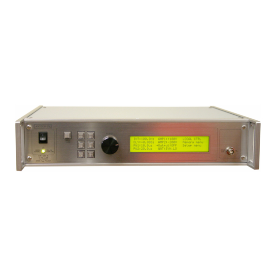
FRONT PANEL CONTROLS 1. POWER Switch . This is the main power switch. When turning the instrument on, there is normally a delay of 10 seconds before anything is shown on the main display, as the internal operating system boots up. If the main menu does not appear after 30 seconds, turn off the instrument and leave it off for at least 60 seconds before applying power again. - Page 18 detail. 5. KEYPAD . Control Name Function MOVE This moves the arrow pointer on the display. CHANGE This is used to enter the submenu, or to select the operating mode, pointed to by the arrow pointer. ×10 If one of the adjustable numeric parameters is displayed, this increases the setting by a factor of ten.
-
Page 19: Rear Panel Controls
REAR PANEL CONTROLS GATE TRIG RS-232 CONTROL GPIB Note: some connectors may be in different positions than shown above, depending on the exact combination of options ordered. 1. AC POWER INPUT . An IEC-320 C14 three-pronged recessed male socket is provided on the back panel for AC power connection to the instrument. - Page 20 Ohm terminator is suggested for this purpose.) 6. GPIB Connector . A standard GPIB cable can be attached to this connector to allow the instrument to be computer-controlled. See the “Programming Manual for -B Instruments” for more details on GPIB control. 7.
-
Page 21: Timing Control
TIMING CONTROL BASIC TIMING CONTROL This instrument can be triggered by its own internal clock or by an external TTL trigger signal. In either case, two output channels respond to the trigger: PULSE and SYNC. The PULSE output is a bipolar signal that may either drive a 50 Ohm load, or the test jig described later. - Page 22 100 ns, FIXED SYNC OUT (generated by the 3V, FIXED internal oscillator) DELAY < 0 PW 1 PW 2 AMP1 (+), VARIABLE Mainframe OUT AMP2 (-), VARIABLE Figure B The next figure illustrates the relationship between the signal when an external TTL- level trigger is used: >...
-
Page 23: Trigger Modes
TRIGGER MODES This instrument has four trigger modes: Internal Trigger: the instrument controls the trigger frequency, and generates the clock internally. External Trigger: the instrument is triggered by an external TTL-level clock on the back-panel TRIG connector. Manual Trigger: the instrument is triggered by the front-panel “SINGLE PULSE” pushbutton. -
Page 24: Basic Amplitude Control
BASIC AMPLITUDE CONTROL The basic test arrangement for the AVR-EB4-B is shown in the figure below. The PULSE output on the instrument mainframe is connected to the PULSE input on the test jig (model AVX-TRR-MIX, or a customized variant) using the supplied coaxial cable, and the control cable is connected using the supplied DB-9 cable. -
Page 25: Setting The Amplitude Levels
V A = I DUT × 50Ω where I is the current through the device under test. A 450 Ohm resistance (R ) is present in series with the measurement output. When a 50 Ohm resistance (R ) is installed on the output (by the user), the output voltage will be one-tenth of V due to the resistor-divider effect. -
Page 26: Amplitude Accuracy
words, the I ratio is irrelevant). The capacitance may be so small that it REVERSE IFORWARD becomes impossible to obtain the full -4 Amps of reverse current. Normally, the forward and reverse amplitudes should be set near the maximum values (+100V, -200V). -
Page 27: Accessible Voltages
the reflections, placing them well after the transient where they may be ignored. A 5- meter-long cable is supplied for this purpose. For “soft-switching” diodes, the shortest possible cable length should be used. The 60-cm-long coaxial cable should be used for these applications. When a “soft switching” diode nears the end of its reverse transient, the diode turns off more gradually. -
Page 28: Standard Test Jig Mechanical Aspects
STANDARD TEST JIG MECHANICAL ASPECTS One AVX-TRR-MIX test jig is normally supplied with the mainframe, unless the customer has requested a different or additional test jigs. AVX-TRR-MIX TEST JIG The AVX-TRR-MIX test jig accepts a range of through-hole and axial devices, using pin sockets and spring-loaded pins. - Page 29 The instrument and the DUT will not be damaged if the diode is installed with the incorrect orientation (i.e., with the anode and cathode reversed). However, incorrect waveforms will be generated. The procedure for inserting most axial and TO-220 packages is straightforward. Simply insert the DUT between one of the Anode pin sockets (in the blue area above) and one of the Cathode sockets (in the red area above).
- Page 30 For TO-3 packages with Case = Cathode The anode pin of interest must be inserted into this socket. For dual- diode devices, rotate the TO-3 package so that the desired diode anode is inserted here. This spring pin must contact the underside of This socket and spring the case.
-
Page 31: Typical Results
TYPICAL RESULTS Obtaining meaningful results with the AVR-EB4-B requires care, experience, and an understanding of diode transient behavior and the impact of inductive and capacitive parasitics. To assist the user, typical results for commercially available diodes are provided below. The user should be able to reliably duplicate these results. - Page 32 1N4937 This transient shows a “soft-switching” recovery, and no reflections are observed at the end of the transient, so the 60 cm coaxial cable was used. If the 5 m cable is used, the measured recovery time will be too high, as shown below: 5 V/div ( = 1 A/div), 20 ns/div.
-
Page 33: J5418 Results
J5418 RESULTS The Microsemi J5418 was tested with amplitudes set to +100V and -200V, and with the mainframe connected to the test jig using a 60 cm coaxial cable. The following reverse recovery waveform was obtained at the test jig "OUT" terminal: 5 V/div ( = 1 A/div), 20 ns/div. -
Page 34: 1N4004 Results
5 V/div ( = 1 A/div), 20 ns/div. 20%-80% switching time shown. S/N 11713. 60 cm cable used. In this case, 73.3 ns was measured for +1A/-2A, versus 73.0 ns for +2A/-4A. 1N4004 RESULTS The generic 1N4004 is a very slow 1A, 400V DO-41 fast-recovery rectifier. With the amplitudes set to +100V and -200V, the following reverse recovery waveform is obtained at the test jig "OUT"... -
Page 35: Mur8100E Results
5 V/div ( = 1 A/div), 200 ns/div. 20%-80% switching time shown. S/N 11713. 60 cm cable used. The above waveform shows the transition from a forward current of +2A to a reverse current of -4A. The reverse transient duration exceeds 1 us under these conditions. MUR8100E RESULTS The On Semiconductor MUR8100E is a 8A, 1000V TO-220 ultrafast rectifier. - Page 36 5 V/div ( = 1 A/div), 20 ns/div. 20%-80% switching time shown. S/N 11713. 60 cm cable used. The above waveform shows the transition from a forward current of +2A to a reverse current of -4A. The reverse transient lasts for approximately 90 ns under these conditions.
-
Page 37: Rus460 Results
RUS460 RESULTS The EDI RUS460 is a 5A, 600V DO-204AR ultrafast rectifier. With the amplitudes set to +100V and -200V, the following reverse recovery waveform is obtained at the test jig "OUT" terminal: 5 V/div ( = 1 A/div), 20 ns/div. 20%-80% switching time shown. - Page 38 5 V/div ( = 1 A/div), 20 ns/div. 20%-80% switching time shown. S/N 11713. 60 cm cable used. With the 60 cm cable, the measured recovery time is nearly the same as before, but the reflections overlap the transient. In this case, it is best to use the 5m, to clearly separate the two effects (recovery versus reflections).
-
Page 39: Csd10120 Results
CSD10120 RESULTS The Cree CSD10120 is a state-of-the-art 1200 Volt, 10 Amp TO-220-packaged Silicon Carbide Schottky diode, promoted as a "Zero Recovery Rectifier". The waveform below shows the results obtained with the CSD10120 diode installed in the AVX-TRR-MIX test jig: 5 V/div ( = 1 A/div), 20 ns/div. -
Page 40: Utg8042 Results
5 V/div ( = 1 A/div), 20 ns/div. 20%-80% switching time shown. S/N 11713. 5m cable used. The above waveform shows the transition from a forward current of +0A to a reverse current of -4A, approximately. The reverse transient is nearly unchanged, relative to the case when the forward current was +2A! The CSD10120 datasheet says "this is a majority carrier diode, so there is no reverse recovery charge", and the results above largely support this. - Page 41 5 V/div ( = 1 A/div), 20 ns/div. 20%-80% switching time shown. S/N 11713. 5m cable used. The above waveform shows the transition from a forward current of +2A to a reverse current of -4A. The reverse transient lasts for approximately 41 ns under these conditions, and then ends rather abruptly, causing reflections.
-
Page 42: Specialized Test Jigs
SPECIALIZED TEST JIGS AVX-TRR-ANB, AXIAL NO-BEND JIG The AVX-TRR-ANB test jig accepts two types of packages: ● DO-41 (0.205" x 0.107" body, maximum) ● Microsemi Axial Type E (0.185" x 0.135" body, maximum) The DUT is installed in the test jig by dropping it over the area marked “DUT” on the test jig PCB. -
Page 43: Avx-Trr-Axpost Jig
The instrument and the DUT will not be damaged if the diode is installed with the incorrect orientation (i.e., with the anode and cathode reversed). However, incorrect waveforms will be generated. When closed, the lid is held is place by a magnetic latch. To open the lid, simply pull upwards on the handle at the front of the lid. -
Page 44: Avx-Trr-Hpost Jig
AVX-TRR-HPOST JIG This is similar to the AVX-TRR-AXPOST jig, except that the axial device is secured with screws, rather than spring-loaded jaws: This provides for slightly lower parasitic inductance, at the expense of convenience. AVX-TRR-MELF, MELF JIG The AVX-TRR-MELF accepts MELF (Metal Electrode Leadless Face) type SMT packages. - Page 45 The next photo shows a MELF device installed between the two pins: A MELF-packaged Device Under Test (DUT)
-
Page 46: Avx-Trr-Melf, Chip-Level Tests
AVX-TRR-MELF, CHIP-LEVEL TESTS Certain test jigs, including the AVX-TRR-MELF, accept chip-level packages. These test jigs use spring-loaded flat-headed probe pins to contact the device under test. The connection arrangement is the same as for the standard test jig. An example of this arrangement is shown below: A chip DUT sandwiched between... - Page 47 To install the diode, spread apart one pair of spring pins with your fingers or tweezers, and insert one end of the diode. Repeat on the other end. This diode produced the following results (t = 341.9 ns): 5 V/div ( = 1 A/div), 200 ns/div. 20%-80% switching time shown.
- Page 48 This diode produced the following results (t = 2.595 us): 5 V/div ( = 1 A/div), 200 ns/div. 20%-80% switching time shown. S/N 11713. 60 cm cable used.
-
Page 49: Avx-Trr-Bta Test Jig
AVX-TRR-BTA TEST JIG The AVX-TRR-BTA test jig is designed to accept the unusual package shown below: The AVX-TRR-BTA test jig is shown below: The DUT is installed by pulling back on the chrome knob, as shown below:... - Page 50 The DUT is then placed on its side in the area immediately in front of the two fixed probe points, as shown in the photo above. Then slowly release the chrome knob, allowing the spring-loaded PCB to push the DUT into position against the two probe points, as shown below.
-
Page 51: Avx-Trr-Sda Test Jig
The anode pad must contact the left probe point, and the cathode pin must contact the right probe point. With a user-supplied device (part number unknown) installed in the AVX-TRR-BTA, and with the amplitudes set to generate I = +2A and I = -4A, the following results were obtained: 5 V/div ( = 1 A/div), 100 ns/div. - Page 52 The device pin sockets and spring pins are shown in greater detail below for the TO-5: Clearance hole for unused TO-5 pin TO-5 Anode TO-5 Cathode Pin Socket Pin Socket Clearance hole for unused TO-5 pin...
- Page 53 Two pin sockets are provided in the central area to accept the TO-5 package. The unconnected pin passes through one of two clearance hole in the PCB. The Anode and Cathode pin sockets are clearly marked on the PCB. The anode pin socket is on the left, and the cathode is on the right.
- Page 54 An installed case-cathode device is shown below: For the case-anode configuration, this layout is used: No connection (for physical support of the TO-3 pin) Spring pin connects TO-3 No connection case to Anode (for physical support of the TO-3 case) Pin socket for TO-3 Cathode pin...
- Page 55 An installed case-anode device is shown below: Only one of the two pins on the TO-3 package is electrically connected in this jig. This allows testing of dual-diode TO-3 packages, by rotating the package to isolate the desired diode. The Microsemi UTG8042 is a dual ultrafast rectifier in a TO-3 package, with the cathodes connected to the case.
-
Page 56: Avx-Trr-Ar1 Test Jig
5 V/div ( = 1 A/div), 40 ns/div. 20%-80% switching time shown. S/N 12584. 60 cm cable used. The above waveform shows the transition from a forward current of +2A to a reverse current of -4A. The reverse transient lasts for approximately 43 ns under these conditions, and then ends rather abruptly, causing small reflections. - Page 57 Then open the tan-colored DUT socket by flipping forward the two black latches on the front edge of it:...
- Page 58 Insert a diode into one of the 4 “pockets”. The two gold contact pins are visible in each pocket; the device must be aligned with these pins. A DO-41 package is shown installed below: Or, shown in a closer view: The remaining photos shown the different types of SQMELF packages installed:...
- Page 59 The four pockets are wired in parallel. Only one DUT may be installed at a time, or the resulting waveforms will be incorrect.
-
Page 60: Avx-Trr-Do214Ac Test Jig
Once the DUT is installed in the appropriate pocket, close the tan-colored socket lid and the black main lid. Both must be closed for proper operation. The instrument and the DUT will not be damaged if the diode is installed with the incorrect orientation (i.e., with the anode and cathode reversed). - Page 61 The next photo shows a DO214AC device (Vishay US1M) installed in the middle pocket. The anode and cathode sides are clearly marked on the PCB. A DO214AC-packaged Device Under Test (DUT)
-
Page 62: Troubleshooting
TROUBLESHOOTING If you obtain “strange” output waveforms, or unexpected values of t , keep these points in mind: 1) The test jig output must be terminated with 50 Ohms. 2) The coaxial cable connecting the test jig to the output module should normally be as short as possible (60 cm or less). -
Page 63: Programming Your Pulse Generator
PROGRAMMING YOUR PULSE GENERATOR KEY PROGRAMMING COMMANDS The “Programming Manual for -B Instruments” describes in detail how to connect the pulse generator to your computer, and the programming commands themselves. A large number of commands are available; however, normally you will only need a few of these. -
Page 64: All Programming Commands
These commands will satisfy 90% of your programming needs. ALL PROGRAMMING COMMANDS For more advanced programmers, a complete list of the available commands is given below. These commands are described in detail in the “Programming Manual for -B Instruments”. (Note: this manual also includes some commands that are not implemented in this instrument. - Page 65 :COUNT? [query only] :VERSion? [query only] TRIGger: :SOURce INTernal | EXTernal | MANual | HOLD | IMMediate *CLS [no query form] *ESE <numeric value> *ESR? [query only] *IDN? [query only] *OPC *SAV 0 | 1 | 2 | 3 [no query form] *RCL 0 | 1 | 2 | 3 [no query form]...
-
Page 66: Mechanical Information
There are no user-adjustable internal circuits. For repairs other than fuse replacement, please contact Avtech (info@avtechpulse.com) to arrange for the instrument to be returned to the factory for repair. Service is to be performed solely by qualified service personnel. -
Page 67: Maintenance
MAINTENANCE REGULAR MAINTENANCE This instrument does not require any regular maintenance. On occasion, one or more of the four rear-panel fuses may require replacement. All fuses can be accessed from the rear panel. See the “FUSES” section for details. CLEANING If desired, the interior of the instrument may be cleaned using compressed air to dislodge any accumulated dust. -
Page 68: Wiring Diagrams
WIRING DIAGRAMS WIRING OF AC POWER M a ins circuits - ha z ard ou s live . A3 - BLACK Do not attem pt any repairs on this instrument POWER SWITCH SW325-ND (CW INDUSTRIES G RS-4022-0013) bey ond the fuse replacement procedures described NORMALLY: ECP180PS24 in the m anual. -
Page 69: Pcb 158R5 - Low Voltage Power Supply
PCB 158R 5 - LOW VOLTAGE POWER SUPPLY... -
Page 70: Pcb 168B - High Voltage Dc Power Supply
PCB 168B - HIGH VOLTAGE DC POWER SUPPLY 1 N4 9 3 7 1 N4 9 3 7 HV WA RN ING HV WA RN ING 6 4 04 4 5 -2 6 4 04 4 5 -2 1 N49 3 7 1 N4 9 3 7 1 0 0 OY R1 0... -
Page 71: Pcb 104G - Keypad / Display Board
PCB 104G - KEYPAD / DISPLAY BOARD... -
Page 72: Main Wiring
MAIN WIRING 1/4A24-P30-ME, WITH PCB 168B J234-ND SPACERS X2 OLO GND +24V, OLO R7 = 5K 3266W D2 = 1N4937A R8 = 100 OY R6 = 3.9K D3 = 1N4937A R9 = R4 = NOT USED D4 = NOT USED R10 = NOT USED R5 =... -
Page 73: Standard Test Jig Wiring (Avx-Trr-Mix)
STANDARD TEST JIG WIRING (AVX-TRR-MIX) K E Y P A D 1 S W 1 D B 9 P I N 1 S W 1 D B 9 P I N 6 R E F L -C D B 9 P I N 2 R E F L -E D B 9 P I N 7 N / C... -
Page 74: Test Jig Wiring (Avx-Trr-Ar1)
TEST JIG WIRING (AVX-TRR-AR1) KE YPA D1 SW 1 SW 1 RE FL-C RE FL-E RE FL-A RE FL-K 1 0 PIN HEA DE R, O N BO TTO M HO A1 3 9 7 REF LECT IV E S ENSO R DU T1 HV A IN GN D... -
Page 75: Test Jig Wiring (Avx-Trr-Axpost)
TEST JIG WIRING (AVX-TRR-AXPOST) K E Y P A D 1 S W 1 D B 9 P I N 1 S W 1 D B 9 P I N 6 R E F L -C D B 9 P I N 2 R E F L -E D B 9 P I N 7 N / C... -
Page 76: Test Jig Wiring (Avx-Trr-Hpost)
TEST JIG WIRING (AVX-TRR-HPOST) -
Page 77: Test Jig Wiring (Avx-Trr-Scha / Avx-Trr-Msb-Melf)
TEST JIG WIRING (AVX-TRR-SCHA / AVX-TRR-MSB-MELF) K E Y P A D 1 S W 1 S W 1 R E F L - C R E F L - E N / C N / C N / C R E F L - A R E F L - K 1 0 P I N H E A D E R... -
Page 78: Test Jig Wiring (Avx-Trr-Scha / Avx-Trr-Msb-Stud)
TEST JIG WIRING (AVX-TRR-SCHA / AVX-TRR-MSB-STUD) K E Y P A D 1 S W 1 S W 1 R E F L - C R E F L - E N / C N / C N / C R E F L - A R E F L - K 1 0 P I N H E A D E R... -
Page 79: Test Jig Wiring (Avx-Trr-Bta)
TEST JIG WIRING (AVX-TRR-BTA) X 1 3 X 1 7 4 - 4 0 M O U N T 1 / 2 I N C H P A D W M B E R G S P R 1 0 - 9 S P R I N G X 1 4 X 1 8 4 - 4 0 M O U N T 1 / 2 I N C H P A D... -
Page 80: Test Jig Wiring (Avx-Trr-Anb)
TEST JIG WIRING (AVX-TRR-ANB) X 2 8 X 3 0 X 2 2 X 2 3 X 2 4 X 2 5 K E Y S T O N E 6 2 1 B R A C K E T K E Y S T O N E 6 2 1 B R A C K E T K E Y S T O N E 6 2 1 B R A C K E T K E Y S T O N E 6 2 1 B R A C K E T... -
Page 81: Test Jig Wiring (Avx-Trr-Sda)
TEST JIG WIRING (AVX-TRR-SDA) K E Y P A D 1 S W 1 D B 9 P I N 1 S W 1 D B 9 P I N 6 R E F L - C D B 9 P I N 2 R E F L - E D B 9 P I N 7 N / C... -
Page 82: Test Jig Wiring (Avx-Trr-Lorax, Avx-Trr-Ssda, Avx-Trr-Do214Ac)
TEST JIG WIRING (AVX-TRR-LORAX, AVX-TRR-SSDA, AVX-TRR-DO214AC) K E Y P A D 1 S W 1 D B 9 P I N 1 S W 1 D B 9 P I N 6 R E F L - C D B 9 P I N 2 R E F L - E D B 9 P I N 7 N / C... -
Page 83: Performance Check Sheet
PERFORMANCE CHECK SHEET...
Need help?
Do you have a question about the AVR-EB4-B and is the answer not in the manual?
Questions and answers