Texas Instruments MSP430 Manual
Hide thumbs
Also See for MSP430:
- Student manual (398 pages) ,
- User manual (194 pages) ,
- Application report (30 pages)
Table of Contents
Advertisement
Quick Links
Texas Instruments (TI) is a well-known US-based semiconductor manufacturer. TI is perhaps best
known to many as the manufacturer of some of the fanciest scientific calculators in the market. Of the
long list of electronic devices produced by TI, microcontrollers are on the top. TI manufactures some
of the coolest and advanced microcontrollers of the market today. There are several categories of
micros from TI. These include general purpose low power MCUs which mainly comprise of MSP430s,
ARMs like TM4Cs, MSP432s, etc, micros for wireless communications like CC2xxx series, ARM + DSP
micros, DSP-specialized micros like the TMS32xxx series and so on. It will look as if TI is committed
toward mixed signal microcontrollers that are engineered for highly sophisticated industrial
challenges. This issue will cover an insight of value-line MSP430 general purpose micros.
MSP430s are not seen as much as the popular 8051s, PICs and AVRs. In most of the Asian market, for
example, MSP430s are rare when compared to other microcontrollers and even still rare when
compared to other chips produced by TI itself. I don't know why there is such an imbalance. Perhaps
one big reason is its inclination towards low power consumption and limited resources. Low-power
means that these MCUs are crafted for special low power applications unlike most other micros.
Secondly TI micros are a bit expensive than other micros. Despites these, TI has provided some great
tools for making things simple. You can get your hands on some cool MSP430 chips through some
affordable Launchpad boards and still it worth every penny learning MSP430s. Firstly, it is a family of
ultra-low power high performance 16-bit (16-bit data bus) micros which are unlike the popular 8-bit
platforms. Secondly MSP430s have highly rich internal hardware peripherals that are second to none.
For instance, MSP430s can be operated over a wide voltage and frequency ranges. Another great
feature that is less common in most 8-bit micros is the DMA controller. Fortunately, MSP430s possess
this. Probably it is your first such micro family that is somewhere between 8-bit and 32-bit micros. In
the end, MSP430s will surely give you a taste of absolute American technology and concepts.
1
Advertisement
Chapters
Table of Contents

Related Manuals for Texas Instruments MSP430


Summary of Contents for Texas Instruments MSP430
- Page 1 Secondly TI micros are a bit expensive than other micros. Despites these, TI has provided some great tools for making things simple. You can get your hands on some cool MSP430 chips through some affordable Launchpad boards and still it worth every penny learning MSP430s. Firstly, it is a family of ultra-low power high performance 16-bit (16-bit data bus) micros which are unlike the popular 8-bit platforms.
- Page 2 MSP430s and 32-bit ARM architecture and as of this moment this series is the most recent development in the MSP430 family. CC430 series is a small series of MSP430s with almost all features one can find in a typical MSP430 micro and embedded sub-GHz radio transceievers. They are well-stuffed true System-on-Chip (SOC) solutions that remove the necessity of additional off-board wireless solutions.
- Page 3 Note that there are some other MSP430 devices that are not accounted here. These devices are either rare or subset of the mentioned families. If you want to know more about MSP430s then you can read...
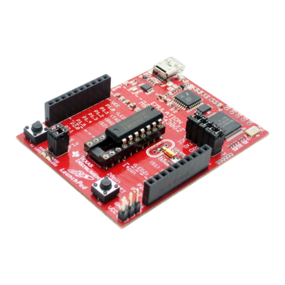
- Page 4 Launchpad Boards and BoosterPacks Launchpad boards are affordable MSP430 evaluation kits. For just few dollars, you can have your own Launchpad boards. They are so cheap that an average school-going student can afford one with his/her own pocket money. However, this cheapness doesn’t compromise quality nor performance.
- Page 5 However due to cheapness and relatively good availability Launchpad boards are by far most popular, particularly the MSP-EXP430G2 Experimenter’s Launchpad board. This board comes boxed with two micros – MSP430G2452 and MSP430G2553. Both of these mixed- signal MCUs come in PDIP packages. We can take them off from the board and use them in bread boards, strip boards, PCBs, etc.
- Page 6 (also known as BoosterPack connectors), onboard power supply, USB-to-serial converter and programming interfaces. MSP430s are ultra-low power 16-bit general purpose microcontrollers. A MSP430 micro consists of a 16-bit RISC CPU, wide variety of feature-rich peripherals and a flexible clock system all under the hood of a von-Neumann architecture.
- Page 7 Shown below is a comparison table of some common MSP430 chips usually found with Launchpad boards. Other Launchpad boards contain other chips but fortunately they share the same pin layout and so they are fully pin compatible. The fourteen pin parts and twenty pin parts share the same pin layout...
- Page 8 From the schematic, we can see what has been placed on the board by default. Parts labelled DNP are not placed on a fresh Launchpad board. These have been left for the users. If these don’t matter much and you need something simpler, then there are Arduino-like pin maps for Launchpads.
- Page 9 Hardware We will obviously need a MSP430 Launchpad board. For this tutorial, I used MSP-EXP430G2 Launchpad board with MSP430G2553 and MSP430G2452 microcontrollers. Apart from the Launchpad board, we will need basic tools like a digital multimeter (DMM), wires or jumper cables, a power bank and other stuffs typically available in an Arduino starter kit like the RIASpire one shown below.
- Page 10 utilizes pins labelled TEST and RST apart from power pins and so only four wires are needed. Note reset pin should be externally pulled up. Check the diagram below. Similarly, we don’t need to buy/use any external USB-serial converter for serial communication as the boards come with onboard hardware for this communication.
- Page 11 It is still nice to have one external MSP-FET programmer. FET stands for Flash Emulation Tool and it supports both JTAG and SWD interfaces. FETs are pretty expensive tools. Lastly, I strongly recommend having an oscilloscope or a logic analyser for checking signals and timing- related info.
- Page 12 AVR. The same thing applies for Energia too. Another key limitation of Energia is the fact that not all MSP430 chips are supported by it. Energia is, however, very easy to use, quick and useful for rapid prototyping or testing. The costs are low overall efficiency and larger code size.
- Page 13 Additionally, some more software tools are needed for supportive purposes. Proteus VSM is a good interactive simulator cum PCB design software. Luckily it supports MSP430 micros. However, it is very expensive unless you are using a pirated version of it. Frankly speaking, I have never advocated for simulations because simulations do not address the real-world challenges we encounter in a real-life real-time project.
- Page 14 (SPL) of STM8 micros. However, these libraries are only supported for the newest and resource-rich MSP430 microcontrollers like the MSP430F5529LP. This idea of driver libraries is quickly gaining mass popularity and is becoming standard day-by-day for all modern era micros. MSP430Ware can be downloaded for free from http://www.ti.com/tool/mspware.
- Page 15 MSP430F2xx, MSP430G2xx and some FR series micros. However, GRACE only generates register values for small MSP430 micros. For large and advanced MSP430 micros driverlib- based codes are generated instead of register-level codes. The rest is just like coding any other...
- Page 16 As we can see the generated code snippet sets appropriate registers as per our setup in GRACE GUI. GRACE can be downloaded without any charge from TI’s website: http://www.ti.com/tool/GRACE?keyMatch=grace%203&tisearch=Search-EN-Products.
- Page 17 We will also need a separate standalone programmer GUI tool. Why? Because it looks totally stupid to open the heavy CCS software every time to upload a code to a new target after having built the final code for it. For this purpose, we will need UniFlash programmer GUI. UniFlash can be downloaded from http://www.ti.com/tool/uniflash or can be accessed via TI cloud.
- Page 18 • App Notes. Though not mandatory, having a collection of MSP430 application notes is a surplus. These show various ideas and design concepts. Visit TI’s website for these docs. There are some important websites, online communities and forums that are very helpful. Some of the most popular ones are: http://www.43oh.com/...
- Page 19 Starting a New CCS Project Beginning a new CCS project is not too complicated. Provided that CCS is installed in your PC, simply run it. In just a few seconds, CCS’s logo splashes. You’ll be asked for workspace location. Either select an existing workspace if you have one or create a new one.
- Page 20 Next click File >> New >> CCS Project. The following window will show up then:...
- Page 21 Here we just need to setup target MCU, name of the project, compiler version and project type. Keep other options unchanged unless you are sure of your actions. The following window appears after hitting the finish and we are good to go for coding. It is just that simple.
- Page 22 GRACE As stated earlier, GRACE is a graphical configuration tool. It reduces the effort of thoroughly reading datasheets and reference manuals. I highly recommend using it no matter if you are novice or expert. First run GRACE. Wait for it to launch. TI’s Resource Explorer kicks in on first start up.
- Page 23 You’ll be prompted for project location, MCU part number and project name as shown below: Once all the parameter fields are filled, we are ready to configure our target MCU. A welcome screen shows up next. From the welcome screen, we have to click on Device Overview and get an insight of the device’s peripherals as peripheral blocks.
- Page 24 We can now click desired hardware peripheral block (blue blocks) to check what features and code examples it offers and set it up as required. There are two types of setups for all modules - Basic and Power users. Basic User setup is for simple setup when you don’t know everything of a peripheral in details and don’t want to mess things up.
- Page 25 UniFlash Most of the times during development, a separate standalone programmer software is not a compulsory necessity as CCS IDE provides an inbuilt programmer/debugger interface. However, at times long after final application development, it becomes completely unnecessary to reopen CCS just to load a firmware to a new micro.
- Page 26 From here we need to select either target board or target microcontroller. No need to type the whole part number of a micro, just few digits/letters are enough to find the correct micro: Similarly, we need to setup connection to target too. USB1 - the first option is what we need to select. Now we are ready to begin firmware upload.
- Page 27 Browse the firmware you wish to upload. You can optionally set some more parameters for the target as shown: To flash new firmware, just hit the Load Image button. Watch this video for details: https://www.youtube.com/watch?v=4uwQSSX-HrM.
- Page 28 Strategies and Tactics Before we begin exploring MSP430 micros, I would like to discuss certain things though they may look like advanced stuffs for the moment. Generating HEX Output Files By default, CCS doesn’t generate any hex formatted output file. Everyone working in the embedded system sector is familiar with it.
- Page 29 Navigate to find MSP430 Hex Utility and then enable it as shown below. Finally select hex output format as shown: Select Intel hex format as it is the one widely used. Having set as shown, from now on, whenever you build your current project, you’ll get an output .hex...
- Page 30 • Header file should contain definitions, variables, constants and function prototypes only. • Header files should begin with the inclusion of MSP430 header file. • Source files should include their respective header files and addition header files (if any). •...
- Page 31 Adding Custom Library Files Adding own developed libraries to a project is key requirement for any software developer. This is because no compiler includes libraries for all hardware. We must realize a compiler as a tool only. The rest is how we use it and what we do with it. As for example, CCS comes with _delay_cycles instead of more commonly preferred delay_ms or delay_us functions.
- Page 32 We need to go to Project >> Properties first and then navigate to Include Options menu under Build >> MSP430 Compiler menu as shown: Right after clicking the circled icon as shown above, we will be asked for folder location. It is just a...
- Page 33 To use the libraries we added, we now just need to add some #include statements in our main.c file. Be careful about the hierarchial order of library files because they may be interdependent. For example, as shown above, the LCD library has dependency on software delay library and so the delay library is added or called before the LCD library.
- Page 34 My code examples will give you an idea of what to copy. Keep in mind to stop the watchdog timer in the beginning of your code or it may reset your micro before entering actual application. Optional Customizations Explore the IDE Preferences for customizing CCS IDE according to your wishes. For instance, unlike the default white theme, I like a full black IDE interface like the one in Sublime Text.
- Page 35 • Try to follow compiler advices and optimizations. Study the MSP430 header files if you can. • You can straight include the header file of your target MCU like as shown below if code cross compatibility among different MCUs of the same group like MSP430x2xx is not needed: #include <msp430g2553.h>...
- Page 36 Basic Clock System Plus (BCS+) In all microcontrollers, power consumption and operating speed are interdependent and it is needed to balance these well to maximize overall performance while conserving energy. MSP430s are crafted with ultra-low power consumption feature in mind while not compromising performance. For this reason, MSP430s are equipped with a number of clock sources that vary in speed, accuracy and area of use.
- Page 37 After having a sneak-a-peek of the MSP430’s clock system, we have to know some basic rules of using the BCS+ module of MSP430G2xx devices: • XT2CLK and LFXT1CLK high frequency mode are both unavailable. We can’t use them. • DCOCLK is the most reliable clock source and should be used for both MCLK and SMCLK.
- Page 38 WDTPW | WDTHOLD; /* initialize Config for the MSP430 GPIO */ GPIO_graceInit(); /* initialize Config for the MSP430 2xx family clock systems (BCS) */ BCSplus_graceInit(); /* initialize Config for the MSP430 System Registers */ System_graceInit(); /* initialize Config for the MSP430 WDT+ */ WDTplus_graceInit();...
- Page 39 * apply new RSELx values. Finally, apply new DCOx and MODx bit values. DCOCTL = 0x00; BCSCTL1 = CALBC1_1MHZ; /* Set DCO to 1MHz */ DCOCTL = CALDCO_1MHZ; * Basic Clock System Control 1 * XT2OFF -- Disable XT2CLK * ~XTS -- Low Frequency * DIVA_0 -- Divide by 1 * Note: ~XTS indicates that XTS has value zero BCSCTL1...
- Page 40 /* Port 2 Direction Register */ P2DIR = 0; /* Port 2 Interrupt Edge Select Register */ P2IES = 0; /* Port 2 Interrupt Flag Register */ P2IFG = 0; /* Port 3 Output Register */ P3OUT = 0; /* Port 3 Direction Register */ P3DIR = 0;...
- Page 41 // Clear OSC fault flag IFG1 &= ~OFIFG; // 50us delay __delay_cycles(25); while (IFG1 & OFIFG); * SR, Status Register * ~SCG1 -- Disable System clock generator 1 * ~SCG0 -- Disable System clock generator 0 * ~OSCOFF -- Oscillator On * ~CPUOFF -- CPU On * GIE -- General interrupt enable * Note: ~<BIT>...
- Page 42 Another odd but important thing you may notice is the fact that the VDD value in MSP430 Launchpads is 3.6V instead of the more commonly used 3.3V. This is the maximum recommended VDD value although MSP430s can tolerate voltages up to 4.0V.
- Page 43 Demo Demo video: https://www.youtube.com/watch?v=gHDibVxfegU.
- Page 44 MSP430s, just like any micro, have digital I/Os for general-purpose input-output operations. The resources and features of MSP430 digital I/Os are very rich and more or less comparable to a typical ARM microcontroller. All I/O can be independently programmed. Many I/Os have external interrupt feature.
- Page 45 WDTPW | WDTHOLD; /* initialize Config for the MSP430 GPIO */ GPIO_graceInit(); /* initialize Config for the MSP430 2xx family clock systems (BCS) */ BCSplus_graceInit(); /* initialize Config for the MSP430 System Registers */ System_graceInit(); /* initialize Config for the MSP430 WDT+ */ WDTplus_graceInit();...
- Page 46 * Note: ~<BIT> indicates that <BIT> has value zero BCSCTL2 SELM_0 DIVM_0 | DIVS_0; (CALBC1_1MHZ 0xFF) { /* Follow recommended flow. First, clear all DCOx and MODx bits. Then * apply new RSELx values. Finally, apply new DCOx and MODx bit values. DCOCTL = 0x00;...
- Page 47 P1IFG = 0; /* Port 2 Output Register */ P2OUT = 0; /* Port 2 Direction Register */ P2DIR = 0; /* Port 2 Interrupt Edge Select Register */ P2IES = 0; /* Port 2 Interrupt Flag Register */ P2IFG = 0;...
- Page 48 /* USER CODE END (section: RTC_B_graceInit_prologue) */ * WDTCTL, Watchdog Timer+ Register * WDTPW -- Watchdog password * WDTHOLD -- Watchdog timer+ is stopped * ~WDTNMIES -- NMI on rising edge * ~WDTNMI -- Reset function * ~WDTTMSEL -- Watchdog mode * ~WDTCNTCL -- No action * ~WDTSSEL -- SMCLK * ~WDTIS0 -- Watchdog clock source bit0 disabled...
- Page 49 • Unused digital I/Os can be left unconnected and floating although it is not wise to do so. • The same applies for oscillator pins. By default, GRACE treats them as oscillator pins. • I/Os are not 5V tolerant. Some sort of mechanism must be applied when using 5V devices. •...
- Page 50 A MSP430 micro in sleep/idle mode consumes literally no energy at all and that is why they are the best micros for battery-backed low power applications.
- Page 51 WDTPW | WDTHOLD; /* initialize Config for the MSP430 GPIO */ GPIO_graceInit(); /* initialize Config for the MSP430 2xx family clock systems (BCS) */ BCSplus_graceInit(); /* initialize Config for the MSP430 System Registers */ System_graceInit(); /* initialize Config for the MSP430 WDT+ */ WDTplus_graceInit();...
- Page 52 /* User initialization code */ /* USER CODE END (section: BCSplus_graceInit_prologue) */ * Basic Clock System Control 2 * SELM_0 -- DCOCLK * DIVM_0 -- Divide by 1 * ~SELS -- DCOCLK * DIVS_0 -- Divide by 1 * ~DCOR -- DCO uses internal resistor * Note: ~<BIT>...
- Page 53 P1OUT = 0; /* Port 1 Direction Register */ P1DIR BIT0 | BIT6; /* Port 1 Interrupt Edge Select Register */ P1IES = BIT3; /* Port 1 Interrupt Flag Register */ P1IFG = 0; /* Port 1 Interrupt Enable Register */ P1IE = BIT3;...
- Page 54 * Note: ~<BIT> indicates that <BIT> has value zero __bis_SR_register(GIE); /* USER CODE START (section: System_graceInit_epilogue) */ /* User code */ /* USER CODE END (section: System_graceInit_epilogue) */ void WDTplus_graceInit(void) /* USER CODE START (section: RTC_B_graceInit_prologue) */ /* User initialization code */ /* USER CODE END (section: RTC_B_graceInit_prologue) */ * WDTCTL, Watchdog Timer+ Register * WDTPW -- Watchdog password...
- Page 55 Explanation The basic theme and the hardware setup for this demo is same as that of the previous one. The only difference is the Launchpad user button. Rather than using polling method, external interrupt method is used. When P1.3 detects a falling edge, P1.0’s state is altered while P1.6 toggles independently in the main loop, denoting two separate independent processes at work simultaneously.
- Page 56 Alphanumeric LCD Alphanumeric LCDs are popular for projecting data and information quickly and efficiently. To use them, we do not need any additional hardware feature in a micro. Digital I/Os are what we need to use these displays. Usually to use these LCDs we need 5V power supply. 3.3V versions of these LCD are rare on the other hand.
- Page 57 Similarly, alphanumeric LCDs also have operating frequency limit. Usually it is about 250 kHz. Refer to the datasheet of the LCD you are using. If the digital I/Os are faster than this max limit value, it is highly likely that the LCD won’t show any valid data at all or it will show up garbage characters.
- Page 58 Code Example delay.h #include <msp430.h> #define F_CPU void delay_us(unsigned int value); void delay_ms(unsigned int value); delay.c #include "delay.h" void delay_us(unsigned int value) register unsigned int loops ((F_CPU value) >> while(loops) _delay_cycles(1); loops--; void delay_ms(unsigned int value) while(value) delay_us(1000); value--; lcd.h #include <msp430.h>...
- Page 59 #define LCD_RS_LOW LCD_PORT &= ~LCD_RS #define LCD_EN_HIGH LCD_PORT |= LCD_EN #define LCD_EN_LOW LCD_PORT &= ~LCD_EN #define LCD_DB4_HIGH LCD_PORT |= LCD_DB4 #define LCD_DB4_LOW LCD_PORT &= ~LCD_DB4 #define LCD_DB5_HIGH LCD_PORT |= LCD_DB5 #define LCD_DB5_LOW LCD_PORT &= ~LCD_DB5 #define LCD_DB6_HIGH LCD_PORT |= LCD_DB6 #define LCD_DB6_LOW LCD_PORT &= ~LCD_DB6...
- Page 60 lcd.c #include "lcd.h" void LCD_init(void) LCD_PORT (LCD_RS LCD_EN LCD_DB4 LCD_DB5 LCD_DB6 | LCD_DB7); delay_ms(20); toggle_EN_pin(); LCD_RS_LOW; LCD_DB7_LOW; LCD_DB6_LOW; LCD_DB5_HIGH; LCD_DB4_HIGH; toggle_EN_pin(); LCD_DB7_LOW; LCD_DB6_LOW; LCD_DB5_HIGH; LCD_DB4_HIGH; toggle_EN_pin(); LCD_DB7_LOW; LCD_DB6_LOW; LCD_DB5_HIGH; LCD_DB4_HIGH; toggle_EN_pin(); LCD_DB7_LOW; LCD_DB6_LOW; LCD_DB5_HIGH; LCD_DB4_LOW; toggle_EN_pin(); LCD_send((_4_pin_interface _2_row_display | _5x7_dots), CMD); LCD_send((display_on cursor_off | blink_off), CMD);...
- Page 61 case CMD: LCD_RS_LOW; break; LCD_4bit_send(value); void LCD_4bit_send(unsigned char lcd_data) toggle_io(lcd_data, 7, LCD_DB7); toggle_io(lcd_data, 6, LCD_DB6); toggle_io(lcd_data, 5, LCD_DB5); toggle_io(lcd_data, 4, LCD_DB4); toggle_EN_pin(); toggle_io(lcd_data, 3, LCD_DB7); toggle_io(lcd_data, 2, LCD_DB6); toggle_io(lcd_data, 1, LCD_DB5); toggle_io(lcd_data, 0, LCD_DB4); toggle_EN_pin(); void LCD_putstr(char *lcd_string) LCD_send(*lcd_string++, DAT); }while(*lcd_string != '\0');...
- Page 62 = 0x00; temp (0x01 & (lcd_data >> bit_pos)); switch(temp) case LCD_PORT &= ~pin_num; break; default: LCD_PORT |= pin_num; break; main.c #include <msp430.h> #include "delay.h" #include "lcd.h" void GPIO_graceInit(void); void BCSplus_graceInit(void); void System_graceInit(void); void WDTplus_graceInit(void); void main(void) unsigned char = 0;...
- Page 63 WDTPW | WDTHOLD; /* initialize Config for the MSP430 GPIO */ GPIO_graceInit(); /* initialize Config for the MSP430 2xx family clock systems (BCS) */ BCSplus_graceInit(); /* initialize Config for the MSP430 System Registers */ System_graceInit(); /* initialize Config for the MSP430 WDT+ */ WDTplus_graceInit();...
- Page 64 /* Port 1 Interrupt Edge Select Register */ P1IES = 0; /* Port 1 Interrupt Flag Register */ P1IFG = 0; /* Port 2 Output Register */ P2OUT = 0; /* Port 2 Port Select Register */ P2SEL &= ~(BIT6 | BIT7);...
- Page 65 * XT2OFF -- Disable XT2CLK * ~XTS -- Low Frequency * DIVA_0 -- Divide by 1 * Note: ~XTS indicates that XTS has value zero BCSCTL1 XT2OFF | DIVA_0; * Basic Clock System Control 3 * XT2S_0 -- 0.4 - 1 MHz * LFXT1S_0 -- If XTS = 0, XT1 = 32768kHz Crystal ;...
- Page 66 * WDTPW -- Watchdog password * WDTHOLD -- Watchdog timer+ is stopped * ~WDTNMIES -- NMI on rising edge * ~WDTNMI -- Reset function * ~WDTTMSEL -- Watchdog mode * ~WDTCNTCL -- No action * ~WDTSSEL -- SMCLK * ~WDTIS0 -- Watchdog clock source bit0 disabled * ~WDTIS1 -- Watchdog clock source bit1 disabled * Note: ~<BIT>...
- Page 67 Explanation Hardly there is a thing to explain here. However, there are a few things to note. After having decided the CPU clock frequency, we must edit the following line of the delay header file to make our delays work as much as accurate as possible: #define F_CPU //CPU Clock in MHz...
- Page 68 Demo Demo video: https://www.youtube.com/watch?v=sJF8oJPu18s.
- Page 69 Of these six modes, three modes are mostly used – Active Mode (AM), LPM0 and LPM3. In Active Mode, the typical self-consumption of a MSP430 device is roughly about 300µA with nothing connected to it. In LPM0 the self-consumption is about a third of active mode while in LPM3, this consumption is just about 1µA.
- Page 70 WDTPW | WDTHOLD; /* initialize Config for the MSP430 GPIO */ GPIO_graceInit(); /* initialize Config for the MSP430 2xx family clock systems (BCS) */ BCSplus_graceInit(); /* initialize Config for the MSP430 System Registers */ System_graceInit(); /* initialize Config for the MSP430 WDT+ */ WDTplus_graceInit();...
- Page 71 P1IES = BIT3; /* Port 1 Interrupt Flag Register */ P1IFG = 0; /* Port 1 Interrupt Enable Register */ P1IE = BIT3; /* Port 2 Output Register */ P2OUT = 0; /* Port 2 Port Select Register */ P2SEL &= ~(BIT6 | BIT7);...
- Page 72 * Basic Clock System Control 1 * XT2OFF -- Disable XT2CLK * ~XTS -- Low Frequency * DIVA_0 -- Divide by 1 * Note: ~XTS indicates that XTS has value zero BCSCTL1 XT2OFF | DIVA_0; * Basic Clock System Control 3 * XT2S_0 -- 0.4 - 1 MHz * LFXT1S_2 -- If XTS = 0, XT1 = VLOCLK ;...
- Page 73 void WDTplus_graceInit(void) /* USER CODE START (section: RTC_B_graceInit_prologue) */ /* User initialization code */ /* USER CODE END (section: RTC_B_graceInit_prologue) */ * WDTCTL, Watchdog Timer+ Register * WDTPW -- Watchdog password * WDTHOLD -- Watchdog timer+ is stopped * ~WDTNMIES -- NMI on rising edge * ~WDTNMI -- Reset function * ~WDTTMSEL -- Watchdog mode * ~WDTCNTCL -- No action...
- Page 74 This is a pretty straight example. The code here works by first flashing the Launchpad board’s red LED for some time. During this time the MSP430 is running in active mode. After the flashing is over, the MP430 micro enters LPM2 state. Note that in LPM2 state all except the DC generator and ACLK are turned off.
- Page 75 Demo Demo video: https://youtu.be/DSRTfoSNDlo.
- Page 76 For storing data like calibration data, settings, etc. that we would have saved in EEPROM memories, we can use the internal flash memory of our MSP430 devices. Though it may sound difficult and challenging, it is not so. However, we need to be very careful about storage locations as such that we don’t accidentally use locations where application codes reside.
- Page 77 /* initialize Config for the MSP430F2xx Flash Memory Controller */ Flash_graceInit(); /* initialize Config for the MSP430 GPIO */ GPIO_graceInit(); /* initialize Config for the MSP430 2xx family clock systems (BCS) */ BCSplus_graceInit(); /* initialize Config for the MSP430 System Registers */ System_graceInit();...
- Page 78 while(1) if((P1IN & BIT3) !BIT3) while((P1IN & BIT3) == !BIT3); Flash_Erase(0x1000); Flash_Write_Char(0x1000, value); lcd_print(13, 1, value); P1OUT |= BIT0; _delay_cycles(40000); P1OUT &= ~BIT0; delay_ms(20); lcd_print(4, 1, value); value++; delay_ms(200); void Flash_graceInit(void) /* USER CODE START (section: Flash_graceInit_prologue) */ /* User initialization code */ /* USER CODE END (section: Flash_graceInit_prologue) */ * Flash Memory Control Register 2 * FSSEL_1 -- MCLK...
- Page 79 /* Port 1 Direction Register */ P1DIR = BIT0; /* Port 1 Resistor Enable Register */ P1REN = BIT3; /* Port 1 Interrupt Edge Select Register */ P1IES = 0; /* Port 1 Interrupt Flag Register */ P1IFG = 0; /* Port 2 Output Register */ P2OUT = 0;...
- Page 80 // Follow recommended flow. First, clear all DCOx and MODx bits. Then // apply new RSELx values. Finally, apply new DCOx and MODx bit values. DCOCTL = 0x00; BCSCTL1 = CALBC1_8MHZ; /* Set DCO to 8MHz */ DCOCTL = CALDCO_8MHZ; * Basic Clock System Control 1 * XT2OFF -- Disable XT2CLK * ~XTS -- Low Frequency...
- Page 81 void WDTplus_graceInit(void) /* USER CODE START (section: RTC_B_graceInit_prologue) */ /* User initialization code */ /* USER CODE END (section: RTC_B_graceInit_prologue) */ * WDTCTL, Watchdog Timer+ Register * WDTPW -- Watchdog password * WDTHOLD -- Watchdog timer+ is stopped * ~WDTNMIES -- NMI on rising edge * ~WDTNMI -- Reset function * ~WDTTMSEL -- Watchdog mode * ~WDTCNTCL -- No action...
- Page 82 __bis_SR_register(GIE); // Enable Interrupts FCTL1 = FWKEY; // Lock FCTL3 FWKEY + LOCK; // Set Lock bit void Flash_Write_Char(unsigned int address, char value) char *FlashPtr (char *)address; FCTL1 FWKEY + WRT; // Set WRT bit for write operation FCTL3 = FWKEY; // Clear Lock bit __bic_SR_register(GIE);...
- Page 83 Simulation Explanation The flash memory module of MSP430s has an integrated controller that controls programming and erase operations. The controller has four registers, a timing generator, and a voltage generator to supply program and erase voltages. Using Grace, we initialize the aforementioned: FCTL2 FWKEY FSSEL_1...
- Page 84 To write a byte, we need two things – memory location and the value we wish to write. This memory location is that piece of memory space where we wish to store the value. void Flash_Write_Char(unsigned int address, char value) char *FlashPtr (char...
- Page 85 The same read-write processes can also be applied to read/write word-level values. The code demoed her works by reading the last data stored in the target flash location (0x1000) and incrementing a variable named value. Only this location is read and updated when the Launchpad board’s button is pressed.
- Page 86 Timer in some case and in other cases, it may be absent. This number is present whenever there are multiple timers of same type in a MSP430 micro. For example, there are two Timer A3s in MSP430G2553 micros and so they are labelled as Timer0_A3 and Timer1_A3. The other number in the timer’s name after the timer type letter denotes the number of CC channels available with it.
- Page 87 Next, we have a prescaler to scale down selected clock source followed by the counter block. What’s interesting about MSP430 timers is the counter’s mode of operation. There are four modes of counter operation and these modes define counting direction: •...
- Page 88 MSP430G2452 has one Timer A3 module and so it has three CC channels. Likewise, MSP430G2553 has six CC channels. When it comes to extreme engineering, TI sometimes seems to overengineer their products. For example, CC channels are not hard fixed to dedicated pins only unlike other micros. Each CC channel has a set of pins associated with it and so they can be remapped if needed.
- Page 89 Input capture is somewhat just the opposite of PWM generation. In capture mode, CC channels can be used to record time-related info of an incoming waveform. A timer in this mode can be left to run on its own. When a waveform edge is detected, the corresponding time count of the timer is stored in CC register.
- Page 90 WDT+ WDT+ is a 15/16-bit watchdog timer. It is mainly intended to prevent unanticipated loops or stuck up conditions due to malfunctions or firmware bugs. The concept behind any watchdog timer is to regularly refresh a counter so that the count never reaches a predefined limit. If due to any reason this limit is exceeded, a reset is issued, causing the host micro to start over again.
- Page 91 Free Running Timer Free running timers are useful in many cases. Free running timers can be used as random number generators, time delay generators, instance markers, etc. Consider the case of time delay generation for instance. Rather than using wasteful CPU-cycle dependent software delay loops, it is much wiser to use a hardware timer to create precise delays and timed events.
- Page 92 WDTPW | WDTHOLD; /* initialize Config for the MSP430 GPIO */ GPIO_graceInit(); /* initialize Config for the MSP430 2xx family clock systems (BCS) */ BCSplus_graceInit(); /* initialize Config for the MSP430 A3 Timer0 */ Timer0_A3_graceInit(); /* initialize Config for the MSP430 System Registers */ System_graceInit();...
- Page 93 /* USER CODE START (section: BCSplus_graceInit_prologue) */ /* User initialization code */ /* USER CODE END (section: BCSplus_graceInit_prologue) */ * Basic Clock System Control 2 * SELM_0 -- DCOCLK * DIVM_0 -- Divide by 1 * ~SELS -- DCOCLK * DIVS_0 -- Divide by 1 * ~DCOR -- DCO uses internal resistor * Note: ~<BIT>...
- Page 94 /* Port 1 Output Register */ P1OUT = 0; /* Port 1 Direction Register */ P1DIR BIT0 | BIT6; /* Port 1 Interrupt Edge Select Register */ P1IES = 0; /* Port 1 Interrupt Flag Register */ P1IFG = 0; /* Port 2 Output Register */ P2OUT = 0;...
- Page 95 * SR, Status Register * ~SCG1 -- Disable System clock generator 1 * ~SCG0 -- Disable System clock generator 0 * ~OSCOFF -- Oscillator On * ~CPUOFF -- CPU On * GIE -- General interrupt enable * Note: ~<BIT> indicates that <BIT> has value zero __bis_SR_register(GIE);...
- Page 96 Simulation Explanation In this demo, Timer_A3 is clocked with SMCLK divided by 8. SMCLK has a frequency of 1MHz and so Timer_A3 is feed with a 125kHz clock. This gives us a timer tick period of 8 microseconds. Since the timer is programmed to operate in continuous mode, i.e.
- Page 97 * TA0CTL, Timer_A3 Control Register * TASSEL_2 -- SMCLK * ID_3 -- Divider - /8 * MC_2 -- Continuous Mode TA0CTL TASSEL_2 ID_3 | MC_2; We want to blink the Launchpad board’s LEDs at the rate of 250 milliseconds. Thus, we need to check or compare if the counter register TA0R has gone past 50% of the full scale 16-bit value.
- Page 98 Demo Demo video: https://www.youtube.com/watch?v=OGvswRhb7ds.
- Page 99 Timer Interrupt We have already seen how to use a timer as a free-running timer. However, in most cases we will need timer interrupts. Timer interrupts are periodic interrupts which means they occur at fixed intervals just like clock ticks. Owing to this nature we can split multiple tasks and make them appear as if all of them are happening concurrently.
-
Page 100: If(Ms
Code Example #include <msp430.h> unsigned int = 0; unsigned int value = 0; unsigned char = 0; unsigned char = 0; const unsigned char num[10] = {0xC0, 0xF9, 0xA4, 0xB0, 0x99, 0x92, 0x82, 0xF8, 0x80, 0x90}; void GPIO_graceInit(void); void BCSplus_graceInit(void);... -
Page 101: Value
&= ~TAIFG; TAIV &= ~TA0IV_TAIFG; void main(void) GPIO_graceInit(); /* initialize Config for the MSP430 2xx family clock systems (BCS) */ BCSplus_graceInit(); /* initialize Config for the MSP430 A3 Timer0 */ Timer0_A3_graceInit(); /* initialize Config for the MSP430 System Registers */ System_graceInit();... - Page 102 /* Port 1 Interrupt Flag Register */ P1IFG = 0; /* Port 2 Output Register */ P2OUT = 0; /* Port 2 Port Select Register */ P2SEL &= ~(BIT6 | BIT7); /* Port 2 Direction Register */ P2DIR BIT0 BIT1 BIT2 BIT3 BIT4...
-
Page 103: Table Of Contents
* Note: ~XTS indicates that XTS has value zero BCSCTL1 XT2OFF | DIVA_0; * Basic Clock System Control 3 * XT2S_0 -- 0.4 - 1 MHz * LFXT1S_0 -- If XTS = 0, XT1 = 32768kHz Crystal ; If XTS = 1, XT1 = 0.4 - 1- MHz crystal or resonator * XCAP_1 -- ~6 pF BCSCTL3... - Page 104 * Note: ~<BIT> indicates that <BIT> has value zero __bis_SR_register(GIE); /* USER CODE START (section: System_graceInit_epilogue) */ /* User code */ /* USER CODE END (section: System_graceInit_epilogue) */ void WDTplus_graceInit(void) /* USER CODE START (section: RTC_B_graceInit_prologue) */ /* User initialization code */ /* USER CODE END (section: RTC_B_graceInit_prologue) */ * WDTCTL, Watchdog Timer+ Register * WDTPW -- Watchdog password...
- Page 105 Explanation In this demo, Timer_A3 is configured as an up counting timer, i.e. it will count from 0 to a top value determined by the contents of TA0CCR0 register. Again, SMCLK is used as the clock source for the timer but this time it is not scaled down. SMCLK is set to 1 MHz and so does Timer_A3. This means every one tick of Timer_A3 is one microsecond in duration.
- Page 106 Everything else in this demo is done inside Timer_A3 interrupt subroutine (ISR). There are two parts inside the ISR. The first as shown below is responsible for counting time. ms++; if(ms > 999) = 0; value++; if(value > 9999) value = 0;...
- Page 107 TA0CTL &= ~TAIFG; TAIV &= ~TA0IV_TAIFG; Demo Demo video: https://www.youtube.com/watch?v=8EG9rcOAATo.
-
Page 108: Case
DAC and so if analogue output is needed, we can use PWM with necessary external RC filtering to create analogue output. A few things must be observed before using MSP430 PWM hardware: • Timer A PWMs are general purpose PWMs. - Page 109 WDTPW | WDTHOLD; /* initialize Config for the MSP430 GPIO */ GPIO_graceInit(); /* initialize Config for the MSP430 2xx family clock systems (BCS) */ BCSplus_graceInit(); /* initialize Config for the MSP430 A3 Timer0 */ Timer0_A3_graceInit(); /* initialize Config for the MSP430 System Registers */ System_graceInit();...
-
Page 110: Basic Clock System Control
/* Port 1 Port Select 2 Register */ P1SEL2 = BIT4; /* Port 1 Output Register */ P1OUT = 0; /* Port 1 Port Select Register */ P1SEL BIT1 BIT4 | BIT6; /* Port 1 Direction Register */ P1DIR BIT1 BIT4 | BIT6;... -
Page 111: Xt2S_0 -- 0.4 - 1 Mhz
(CALBC1_1MHZ 0xFF) { /* Follow recommended flow. First, clear all DCOx and MODx bits. Then * apply new RSELx values. Finally, apply new DCOx and MODx bit values. DCOCTL = 0x00; BCSCTL1 = CALBC1_1MHZ; /* Set DCO to 1MHz */ DCOCTL = CALDCO_1MHZ;... -
Page 112: Ta0Ccr0, Timer_A Capture/Compare Register 0 */ Ta0Ccr0
* CM_0 -- No Capture * CCIS_0 -- CCIxA * ~SCS -- Asynchronous Capture * ~SCCI -- Latched capture signal (read) * ~CAP -- Compare mode * OUTMOD_3 -- PWM output mode: 3 - PWM set/reset * Note: ~<BIT> indicates that <BIT> has value zero TA0CCTL1 CM_0 CCIS_0... -
Page 113: Sr, Status Register * * ~Scg1 -- Disable System Clock Generator
IFG1 &= ~OFIFG; // 50us delay __delay_cycles(50); while (IFG1 & OFIFG); * SR, Status Register * ~SCG1 -- Disable System clock generator 1 * ~SCG0 -- Disable System clock generator 0 * ~OSCOFF -- Oscillator On * ~CPUOFF -- CPU On * GIE -- General interrupt enable * Note: ~<BIT>... - Page 114 Simulation Explanation Just as in the previous example, SMCLK is set to 1MHz. Timer_A3 is also setup for up counting with a top value of 999, resulting in 1ms time duration. Note no interrupt is used and other CCR registers are loaded with 10 –...
- Page 115 Prior to Timer_A3 setup, CC channels are setup. OUTMOD is that stuff that sets PWM type. * TA0CCTL0, Capture/Compare Control Register 0 * CM_0 -- No Capture * CCIS_0 -- CCIxA * ~SCS -- Asynchronous Capture * ~SCCI -- Latched capture signal (read) * ~CAP -- Compare mode * OUTMOD_4 -- PWM output mode: 4 - Toggle * Note: ~<BIT>...
- Page 117 PWMs can be of the following types: Note that CCR0 has limited PWM options and it is the value of its register that sets PWM frequency. The other CCR registers are loaded with values that determine respective PWM duty cycles.
- Page 118 Demo Demo video: https://www.youtube.com/watch?v=dbSPi6LbsQg.
-
Page 119: Case
A module. We can use these channels to capture incoming waveforms of unknown frequencies/duty cycles and have them measured with respect to a known clock like SMCLK. Again a few things must be observed before using MSP430 input capture hardware: •... - Page 120 WDTPW | WDTHOLD; /* initialize Config for the MSP430 GPIO */ GPIO_graceInit(); /* initialize Config for the MSP430 2xx family clock systems (BCS) */ BCSplus_graceInit(); /* initialize Config for the MSP430 A3 Timer0 */ Timer0_A3_graceInit(); /* initialize Config for the MSP430 A3 Timer0 */ Timer1_A3_graceInit();...
- Page 121 /* initialize Config for the MSP430 WDT+ */ WDTplus_graceInit(); LCD_init(); LCD_clear_home(); LCD_goto(0, 0); LCD_putstr("Capt./us:"); delay_ms(10); while(1) if((P1IN & BIT3) P1OUT |= BIT0; while((P1IN & BIT3) == 0); i++; if(i > = 0; P1OUT &= ~BIT0; switch(i) case TA0CCR0 = 9999;...
- Page 122 LCD_putstr("Period/us: 334"); break; case TA0CCR0 = 1230; LCD_goto(0, 1); LCD_putstr("Period/ms: 2.5"); break; case TA0CCR0 = 2626; LCD_goto(0, 1); LCD_putstr("Period/ms: 5.3"); break; case TA0CCR0 = 4579; LCD_goto(0, 1); LCD_putstr("Period/ms: 9.2"); break; case TA0CCR0 = 499; LCD_goto(0, 1); LCD_putstr("Period/ms: 1"); break; default: TA0CCR0 = 6964;...
- Page 123 /* Port 1 Direction Register */ P1DIR BIT0 BIT1 BIT6 | BIT7; /* Port 1 Resistor Enable Register */ P1REN = BIT3; /* Port 1 Interrupt Edge Select Register */ P1IES = 0; /* Port 1 Interrupt Flag Register */ P1IFG = 0;...
- Page 124 BCSCTL2 SELM_0 DIVM_0 | DIVS_0; (CALBC1_1MHZ 0xFF) { /* Follow recommended flow. First, clear all DCOx and MODx bits. Then * apply new RSELx values. Finally, apply new DCOx and MODx bit values. DCOCTL = 0x00; BCSCTL1 = CALBC1_1MHZ; /* Set DCO to 1MHz */ DCOCTL = CALDCO_1MHZ;...
- Page 125 TA0CCR0 = 9999; * TA0CTL, Timer_A3 Control Register * TASSEL_2 -- SMCLK * ID_1 -- Divider - /2 * MC_1 -- Up Mode TA0CTL TASSEL_2 ID_1 | MC_1; /* USER CODE START (section: Timer0_A3_graceInit_epilogue) */ /* User code */ /* USER CODE END (section: Timer0_A3_graceInit_epilogue) */ void Timer1_A3_graceInit(void) /* USER CODE START (section: Timer1_A3_graceInit_prologue) */...
- Page 126 /* USER CODE START (section: Timer1_A3_graceInit_epilogue) */ /* User code */ /* USER CODE END (section: Timer1_A3_graceInit_epilogue) */ void System_graceInit(void) /* USER CODE START (section: System_graceInit_prologue) */ /* User initialization code */ /* USER CODE END (section: System_graceInit_prologue) */ /* Clear oscillator fault flag with software delay */ // Clear OSC fault flag IFG1 &= ~OFIFG;...
-
Page 127: Value
* ~WDTIS1 -- Watchdog clock source bit1 disabled * Note: ~<BIT> indicates that <BIT> has value zero WDTCTL WDTPW | WDTHOLD; /* USER CODE START (section: RTC_B_graceInit_epilogue) */ /* User code */ /* USER CODE END (section: RTC_B_graceInit_epilogue) */ void lcd_print(unsigned char x_pos, unsigned char y_pos,... - Page 128 Explanation For this demo, I used a MSP430G2553 micro as it has two independent timers. One of these timers is used as a waveform generator and the other as a waveform capture unit. Timer0_A3 is set up as a PWM output generator with only CC channel 0 active. CC channel 0 is set just to toggle its output logic states and not duty cycle.
- Page 129 * TA1CCTL0, Capture/Compare Control Register 0 * CM_1 -- Rising Edge * CCIS_0 -- CCIxA * ~SCS -- Asynchronous Capture * ~SCCI -- Latched capture signal (read) * ~CAP -- Compare mode * OUTMOD_1 -- PWM output mode: 1 - Set * Note: ~<BIT>...
- Page 130 In the main loop, we are using the Launchpad’s user button to alter TA0CCR0’s value and hence PWM frequency or period. There are ten different time periods to select. The main code also displays captured waveform time period vs expected time period on a LCD. if((P1IN &...
- Page 131 LCD_putstr("Period/ms: 2.5"); break; case TA0CCR0 = 2626; LCD_goto(0, 1); LCD_putstr("Period/ms: 5.3"); break; case TA0CCR0 = 4579; LCD_goto(0, 1); LCD_putstr("Period/ms: 9.2"); break; case TA0CCR0 = 499; LCD_goto(0, 1); LCD_putstr("Period/ms: 1"); break; default: TA0CCR0 = 6964; LCD_goto(0, 1); LCD_putstr("Period/ms: 13.9"); break; time_period (pulse_ticks >>...
- Page 133 Demo Demo video: https://www.youtube.com/watch?v=CHLkXf8MqbQ.
- Page 134 | BIT6); __bic_SR_register_on_exit(LPM0_bits); void main(void) /* Stop watchdog timer from timing out during initial start-up. */ WDTCTL WDTPW | WDTHOLD; /* initialize Config for the MSP430 GPIO */ GPIO_graceInit(); /* initialize Config for the MSP430 2xx family clock systems (BCS) */...
- Page 135 BCSplus_graceInit(); /* initialize Config for the MSP430 A3 Timer0 */ Timer0_A3_graceInit(); /* initialize Config for the MSP430 System Registers */ System_graceInit(); /* initialize Config for the MSP430 WDT+ */ WDTplus_graceInit(); P1OUT |= BIT0; P1OUT &= ~BIT6; while(1) __bis_SR_register(LPM0_bits); void GPIO_graceInit(void)
- Page 136 void BCSplus_graceInit(void) /* USER CODE START (section: BCSplus_graceInit_prologue) */ /* User initialization code */ /* USER CODE END (section: BCSplus_graceInit_prologue) */ * Basic Clock System Control 2 * SELM_0 -- DCOCLK * DIVM_0 -- Divide by 1 * ~SELS -- DCOCLK * DIVS_0 -- Divide by 1 * ~DCOR -- DCO uses internal resistor * Note: ~<BIT>...
- Page 137 /* USER CODE START (section: Timer0_A3_graceInit_prologue) */ /* User initialization code */ /* USER CODE END (section: Timer0_A3_graceInit_prologue) */ * TA0CCTL0, Capture/Compare Control Register 0 * CM_0 -- No Capture * CCIS_0 -- CCIxA * ~SCS -- Asynchronous Capture * ~SCCI -- Latched capture signal (read) * ~CAP -- Compare mode * OUTMOD_0 -- PWM output mode: 0 - OUT bit value * Note: ~<BIT>...
- Page 138 void WDTplus_graceInit(void) /* USER CODE START (section: RTC_B_graceInit_prologue) */ /* User initialization code */ /* USER CODE END (section: RTC_B_graceInit_prologue) */ * WDTCTL, Watchdog Timer+ Register * WDTPW -- Watchdog password * WDTHOLD -- Watchdog timer+ is stopped * ~WDTNMIES -- NMI on rising edge * ~WDTNMI -- Reset function * ~WDTTMSEL -- Watchdog mode * ~WDTCNTCL -- No action...
- Page 139 source. Note that in the diagram below timer overflow interrupt is not being used. Timer capture- compare interrupt is used instead. The desire time period is set for 400ms or 2.5Hz. At every 400ms interval, a compare-match interrupt will occur. How this is done? Well the timer is set for up counting and it has an input clock of 125kHz –...
- Page 140 * TA0CTL, Timer_A3 Control Register * TASSEL_2 -- SMCLK * ID_3 -- Divider - /8 * MC_1 -- Up Mode TA0CTL TASSEL_2 ID_3 | MC_1; /* USER CODE START (section: Timer0_A3_graceInit_epilogue) */ /* User code */ /* USER CODE END (section: Timer0_A3_graceInit_epilogue) */ Inside the interrupt function, the LEDs of Launchpad board are toggled.
- Page 141 Watchdog Timer Plus (WDT+) At present, any commercial/industrial/professional electronic good must pass a number of tests and obtain some certifications before its introduction to market, most notably CE, FCC, UL and TUV certifications. This is so as it is imperative that a device pass Electromagnetic Compliance (EMC) test not just for flawless performance but also for user safety.
- Page 142 + WDTHOLD; // Set hold bit and clear others /* initialize Config for the MSP430 GPIO */ GPIO_graceInit(); /* initialize Config for the MSP430 2xx family clock systems (BCS) */ BCSplus_graceInit(); /* initialize Config for the MSP430 System Registers */ System_graceInit();...
- Page 143 P1OUT = BIT3; /* Port 1 Direction Register */ P1DIR BIT0 | BIT6; /* Port 1 Resistor Enable Register */ P1REN = BIT3; /* Port 1 Interrupt Edge Select Register */ P1IES = 0; /* Port 1 Interrupt Flag Register */ P1IFG = 0;...
- Page 144 BCSCTL1 = CALBC1_1MHZ; /* Set DCO to 1MHz */ DCOCTL = CALDCO_1MHZ; * Basic Clock System Control 1 * XT2OFF -- Disable XT2CLK * ~XTS -- Low Frequency * DIVA_3 -- Divide by 8 * Note: ~XTS indicates that XTS has value zero BCSCTL1 XT2OFF | DIVA_3;...
- Page 145 /* USER CODE START (section: System_graceInit_epilogue) */ /* User code */ /* USER CODE END (section: System_graceInit_epilogue) */ void WDTplus_graceInit(void) /* USER CODE START (section: RTC_B_graceInit_prologue) */ /* User initialization code */ /* USER CODE END (section: RTC_B_graceInit_prologue) */ * WDTCTL, Watchdog Timer+ Register * WDTPW -- Watchdog password * ~WDTHOLD -- Watchdog timer+ is not stopped * ~WDTNMIES -- NMI on rising edge...
- Page 146 Explanation Unlike previous timer examples, 12 kHz ACLK is used. ACLK is divided by 8 to make it 1.5 kHz low speed clock source for the WDT+ module. This clock is further prescaled by 32768 to get a WDT+ timeout of about 22 seconds.
- Page 147 while(1) P1OUT ^= BIT6; _delay_cycles(45000); In reality, the timeout time may vary due to variations in ACLK time period. In my demo, I noticed this variation. During that time, I found that ACLK is about 10 kHz instead of 12 kHz. Demo Demo video: https://www.youtube.com/watch?v=vYCLeWZZt7U.
- Page 148 WDT+ as an Interval Timer There are cases in which we don’t need the protection feature of WDT+. This leaves with a free timer which can be used for other jobs. As I said before, Americans think differently than the rest of the world and here is one proof of that ingenious concept.
- Page 149 WDTPW | WDTHOLD; /* initialize Config for the MSP430 GPIO */ GPIO_graceInit(); /* initialize Config for the MSP430 2xx family clock systems (BCS) */ BCSplus_graceInit(); /* initialize Config for the MSP430 System Registers */ System_graceInit(); /* initialize Config for the MSP430 WDT+ */ WDTplus_graceInit();...
- Page 150 switch(i) case P1OUT &= ~BIT0; break; default: P1OUT |= BIT0; break; break; case _delay_cycles(1); s++; if(s > 20000) P1OUT ^= BIT6; = 0; break; default: if((P1IN & BIT3) BIT3) ^= BIT0; break; void GPIO_graceInit(void) /* USER CODE START (section: GPIO_graceInit_prologue) */ /* User initialization code */ /* USER CODE END (section: GPIO_graceInit_prologue) */ /* Port 1 Output Register */...
- Page 151 /* Port 1 Interrupt Flag Register */ P1IFG = 0; /* Port 2 Output Register */ P2OUT = 0; /* Port 2 Port Select Register */ P2SEL &= ~(BIT6 | BIT7); /* Port 2 Direction Register */ P2DIR = 0; /* Port 2 Interrupt Edge Select Register */ P2IES = 0;...
- Page 152 * Note: ~XTS indicates that XTS has value zero BCSCTL1 XT2OFF | DIVA_2; * Basic Clock System Control 3 * XT2S_0 -- 0.4 - 1 MHz * LFXT1S_2 -- If XTS = 0, XT1 = VLOCLK ; If XTS = 1, XT1 = 3 - 16-MHz crystal or resonator * XCAP_1 -- ~6 pF BCSCTL3...
- Page 153 * SR, Status Register * ~SCG1 -- Disable System clock generator 1 * ~SCG0 -- Disable System clock generator 0 * ~OSCOFF -- Oscillator On * ~CPUOFF -- CPU On * GIE -- General interrupt enable * Note: ~<BIT> indicates that <BIT> has value zero __bis_SR_register(GIE);...
- Page 154 Simulation Explanation WDT+ is used here as an interval timer with a time period of 512 microseconds. After every 512 microseconds, there is a WDT+ interrupt. * WDTCTL, Watchdog Timer+ Register * WDTPW -- Watchdog password * ~WDTHOLD -- Watchdog timer+ is not stopped * ~WDTNMIES -- NMI on rising edge * ~WDTNMI -- Reset function * WDTTMSEL -- Interval timer mode...
- Page 155 The variable task in the main loop is used to switch between different tasks, each task having same time frame and priority. This is called a task scheduling. switch(task) case switch(i) case P1OUT &= ~BIT0; break; default: P1OUT |= BIT0; break;...
- Page 156 Demo Demo video: https://www.youtube.com/watch?v=BNwxdgLQerU.
- Page 157 The most common ADCs in MSP430s are ADC10 and ADC12. These are Successive Approximation (SAR) ADCs. Both of these ADCs are similar in many aspects except in resolution. Some MSP430 devices have more advanced high-resolution delta-sigma ADCs like SD16_A and SD24_A. All MSP430s additionally have internal temperature sensors.
- Page 158 We can also use them to make filters, oscillators, analogue computers, etc. In this article only ADC10 and COMP_A+ will be discussed. The rest two will be skipped as the MSP430 chips discussed here don’t have any more hardware other than these.
- Page 159 Comp_A+ Module Apart from ADCs MSP430x2xx devices are equipped with an analogue comparator called Comparator A+ or simply Comp_A+ module. Shown above is the block diagram for Comp A+ module. The left most side includes comparator inputs. A good thing to note is that unlike other micros where comparator pins are generally fixed to some dedicated I/Os only, the pins of COMP A+ can be tied with a number of I/O, adding great flexibility in design.
- Page 160 WDTPW | WDTHOLD; /* initialize Config for the MSP430 GPIO */ GPIO_graceInit(); /* initialize Config for the MSP430 2xx family clock systems (BCS) */ BCSplus_graceInit(); /* initialize Config for the MSP430F2xx Comparator_A+ */ Comparator_Aplus_graceInit(); /* initialize Config for the MSP430 System Registers */ System_graceInit();...
- Page 161 /* USER CODE START (section: BCSplus_graceInit_prologue) */ /* User initialization code */ /* USER CODE END (section: BCSplus_graceInit_prologue) */ * Basic Clock System Control 2 * SELM_0 -- DCOCLK * DIVM_0 -- Divide by 1 * ~SELS -- DCOCLK * DIVS_0 -- Divide by 1 * ~DCOR -- DCO uses internal resistor * Note: ~<BIT>...
- Page 162 /* User initialization code */ /* USER CODE END (section: GPIO_graceInit_prologue) */ /* Port 1 Output Register */ P1OUT = 0; /* Port 1 Port Select Register */ P1SEL = BIT7; /* Port 1 Direction Register */ P1DIR BIT0 BIT6 | BIT7;...
- Page 163 /* USER CODE START (section: Comparator_Aplus_graceInit_epilogue) */ /* User code */ /* USER CODE END (section: Comparator_Aplus_graceInit_epilogue) */ void System_graceInit(void) /* USER CODE START (section: System_graceInit_prologue) */ /* User initialization code */ /* USER CODE END (section: System_graceInit_prologue) */ * SR, Status Register * ~SCG1 -- Disable System clock generator 1 * ~SCG0 -- Disable System clock generator 0 * ~OSCOFF -- Oscillator On...
- Page 164 Simulation Explanation For this demo, a MSP430G2553 is used. Launchpad board’s LEDs are used and additionally a potentiometer (pot) is tied to P1.5. The pot has its ends connected to VDD and GND. The internal connection is as shown below: The code dictates that Comp A+ interrupt will occur on falling edges only.
- Page 165 Demo Demo video: https://www.youtube.com/watch?v=XIzvhpWopiI.
- Page 166 ADC10 In most value-line devices (VLD) like MSP430G2553 and MSP430G2452, ADC12 is not present and the ADC tasks are accomplished with ADC10 modules. Shown above is the simple block diagram of the ADC10 module. ADC10 is a SAR ADC. Highlighted segments include: •...
- Page 167 WDTPW | WDTHOLD; /* initialize Config for the MSP430 GPIO */ GPIO_graceInit(); /* initialize Config for the MSP430 2xx family clock systems (BCS) */ BCSplus_graceInit(); /* initialize Config for the MSP430 10-bit Analog to Digital Converter (ADC) ADC10_graceInit(); /* initialize Config for the MSP430 System Registers */ System_graceInit();...
- Page 168 if(n > = 0; P1OUT &= ~BIT6; switch(n) case ADC_Value = get_ADC(INCH_1); = get_volt(ADC_Value); LCD_goto(0, 0); LCD_putstr("ADC Ch01:"); LCD_goto(0, 1); LCD_putstr("Volts/mV:"); break; case ADC_Value = get_ADC(INCH_2); = get_volt(ADC_Value); LCD_goto(0, 0); LCD_putstr("ADC Ch02:"); LCD_goto(0, 1); LCD_putstr("Volts/mV:"); break; default: ADC_Value = get_ADC(INCH_10); = get_temp(get_volt(ADC_Value));...
- Page 169 /* Port 1 Direction Register */ P1DIR BIT0 | BIT6; /* Port 1 Resistor Enable Register */ P1REN = BIT3; /* Port 1 Interrupt Edge Select Register */ P1IES = 0; /* Port 1 Interrupt Flag Register */ P1IFG = 0; /* Port 2 Output Register */ P2OUT = 0;...
- Page 170 (CALBC1_1MHZ 0xFF) { /* Follow recommended flow. First, clear all DCOx and MODx bits. Then * apply new RSELx values. Finally, apply new DCOx and MODx bit values. DCOCTL = 0x00; BCSCTL1 = CALBC1_1MHZ; /* Set DCO to 1MHz */ DCOCTL = CALDCO_1MHZ;...
- Page 171 * ADC10SHT_3 -- 64 x ADC10CLKs * SREF_0 -- VR+ = VCC and VR- = VSS * Note: ~<BIT> indicates that <BIT> has value zero ADC10CTL0 ADC10ON ADC10SHT_3 | SREF_0; * Control Register 1 * ~ADC10BUSY -- No operation is active * CONSEQ_2 -- Repeat single channel * ADC10SSEL_3 -- SMCLK * ADC10DIV_3 -- Divide by 4...
-
Page 172: Value
void WDTplus_graceInit(void) /* USER CODE START (section: RTC_B_graceInit_prologue) */ /* User initialization code */ /* USER CODE END (section: RTC_B_graceInit_prologue) */ * WDTCTL, Watchdog Timer+ Register * WDTPW -- Watchdog password * WDTHOLD -- Watchdog timer+ is stopped * ~WDTNMIES -- NMI on rising edge * ~WDTNMI -- Reset function * ~WDTTMSEL -- Watchdog mode * ~WDTCNTCL -- No action... - Page 173 void lcd_print(unsigned char x_pos, unsigned char y_pos, unsigned int value) char = 0x00; ((value 1000) + 0x30); LCD_goto(x_pos, y_pos); LCD_putchar(chr); (((value 100) + 0x30); LCD_goto((x_pos + 1), y_pos); LCD_putchar(chr); (((value + 0x30); LCD_goto((x_pos + 2), y_pos); LCD_putchar(chr); ((value + 0x30); LCD_goto((x_pos + 3), y_pos);...
- Page 174 Explanation ADC10 is set up initially as depicted below: Note that we are not using ADC10 interrupt and enabled two external channels (A1 and A2) although only the temperature sensor channel is selected for conversion. The internal temperature sensor has the highest channel number (channel 10) after VDD measurement channel (channel 11).
- Page 175 ADC10CTL0 |= ENC; ADC10CTL0 |= ADC10SC; while ((ADC10CTL0 & ADC10IFG) == 0); return ADC10MEM; The function above first disables the momentarily and clears channel number or count. Then the desired channel is chosen. AD conversion is started following ADC restart and we wait for AD conversion completion.
- Page 176 Demo...
- Page 177 Demo video: https://www.youtube.com/watch?v=M_txQs2ajdk.
- Page 178 ADC10 Interrupt In previous example, we didn’t use ADC10 interrupt and the code was based on polling. ADC interrupts are as important as timer interrupts. We can start an ADC and extract conversion data in an orderly manner when conversion is complete. No other process waits for the ADC, freeing up the CPU. Many present-day microcontrollers have on-chip temperature sensors.
-
Page 179: Value
WDTPW | WDTHOLD; /* initialize Config for the MSP430 GPIO */ GPIO_graceInit(); /* initialize Config for the MSP430 2xx family clock systems (BCS) */ BCSplus_graceInit(); /* initialize Config for the MSP430 10-bit Analog to Digital Converter (ADC) ADC10_graceInit(); /* initialize Config for the MSP430 System Registers */ System_graceInit();... - Page 180 LCD_goto(0, 1); LCD_putstr("Tmp/Deg.C:"); while(1) // ADC Start Conversion - Software trigger ADC10CTL0 |= ADC10SC; P1OUT ^= BIT6; = get_volt(ADC_Value); = get_temp(t); lcd_print(12, 0, ADC_Value); lcd_print(12, 1, t); delay_ms(200); void GPIO_graceInit(void) /* Port 1 Output Register */ P1OUT = 0; /* Port 1 Direction Register */ P1DIR BIT0 | BIT6;...
- Page 181 * Basic Clock System Control 2 * SELM_0 -- DCOCLK * DIVM_0 -- Divide by 1 * ~SELS -- DCOCLK * DIVS_0 -- Divide by 1 * ~DCOR -- DCO uses internal resistor * Note: ~<BIT> indicates that <BIT> has value zero BCSCTL2 SELM_0 DIVM_0...
- Page 182 * ~ADC10IFG -- Clear ADC interrupt flag * ADC10IE -- Enable ADC interrupt * ADC10ON -- Switch On ADC10 * ~REFON -- Disable ADC reference generator * ~REF2_5V -- Set reference voltage generator = 1.5V * MSC -- Enable multiple sample and conversion * ~REFBURST -- Reference buffer on continuously * ~REFOUT -- Reference output off * ADC10SR -- Reference buffer supports up to ~50 ksps...
- Page 183 * Note: ~<BIT> indicates that <BIT> has value zero __bis_SR_register(GIE); void WDTplus_graceInit(void) * WDTCTL, Watchdog Timer+ Register * WDTPW -- Watchdog password * WDTHOLD -- Watchdog timer+ is stopped * ~WDTNMIES -- NMI on rising edge * ~WDTNMI -- Reset function * ~WDTTMSEL -- Watchdog mode * ~WDTCNTCL -- No action * ~WDTSSEL -- SMCLK...
- Page 184 Simulation *Note Proteus VSM cannot simulate internal temperature sensor. The simulation here only shows connections. The readouts are misleading. Explanation...
-
Page 185: Value
ADC10 setup is similar to the setup we have seen in the last example. However, this time we enabled ADC10 interrupt as this is an interrupt-based demo. The ADC ISR is simple. Here we are just toggling P1.0 LED to indicate ADC conversion completion and clearing ADC interrupt flag after reading ADC data value. - Page 186 Demo Demo video: https://www.youtube.com/watch?v=XOlI3Vfjfb8.
- Page 187 = 0; unsigned int adc_avg = 0; /* Stop watchdog timer from timing out during initial start-up. */ WDTCTL WDTPW | WDTHOLD; /* initialize Config for the MSP430 GPIO */...
- Page 188 GPIO_graceInit(); /* initialize Config for the MSP430 2xx family clock systems (BCS) */ BCSplus_graceInit(); /* initialize Config for the MSP430 10-bit Analog to Digital Converter (ADC) ADC10_graceInit(); /* initialize Config for the MSP430 System Registers */ System_graceInit(); /* initialize Config for the MSP430 WDT+ */ WDTplus_graceInit();...
- Page 189 /* Port 1 Interrupt Edge Select Register */ P1IES = 0; /* Port 1 Interrupt Flag Register */ P1IFG = 0; /* Port 2 Output Register */ P2OUT = 0; /* Port 2 Direction Register */ P2DIR = 0; /* Port 2 Interrupt Edge Select Register */ P2IES = 0;...
- Page 190 * XT2OFF -- Disable XT2CLK * ~XTS -- Low Frequency * DIVA_0 -- Divide by 1 * Note: ~XTS indicates that XTS has value zero BCSCTL1 XT2OFF | DIVA_0; * Basic Clock System Control 3 * XT2S_0 -- 0.4 - 1 MHz * LFXT1S_2 -- If XTS = 0, XT1 = VLOCLK ;...
- Page 191 * ADC10SSEL_0 -- ADC10OSC * ADC10DIV_0 -- Divide by 1 * ~ISSH -- Input signal not inverted * ~ADC10DF -- ADC10 Data Format as binary * SHS_0 -- ADC10SC * INCH_1 -- ADC Channel 1 * Note: ~<BIT> indicates that <BIT> has value zero ADC10CTL1 CONSEQ_2 ADC10SSEL_0...
- Page 192 * ~SCG0 -- Disable System clock generator 0 * ~OSCOFF -- Oscillator On * ~CPUOFF -- CPU On * GIE -- General interrupt enable * Note: ~<BIT> indicates that <BIT> has value zero __bis_SR_register(GIE); /* USER CODE START (section: System_graceInit_epilogue) */ /* User code */ /* USER CODE END (section: System_graceInit_epilogue) */ void...
- Page 193 ((value + 0x30); LCD_goto((x_pos + 3), y_pos); LCD_putchar(chr); Simulation...
- Page 194 DTC block. Note the starting memory address and the memory block size. The memory we are talking about here is no other than MSP430’s RAM. Unless you want to assign a different pointer address, keep it untouched. So why is it pointed at RAM location 512 (0x200) by default? The answer is the fact that this is first RAM location for our target MSP430G2452 microcontroller.
- Page 195 The block size indicates that number of locations that we will need to store ADC10 data. MSP430s are 16-bit microcontrollers and since ADC10 gives 10-bit data, we need sixteen word-sized (16-bit) locations to store sixteen ADC samples. These 16 samples are to be averaged. #define no_of_samples ..
- Page 196 Demo Demo video: https://youtu.be/0V2zOTRwPKI.
-
Page 197: Value
We have seen in the last segment that how we can compute the average value of an ADC10 channel without involving the CPU much and using the MSP430’s DMA/DTC controller. The DTC of MSP430s can be used in many innovative ways. One such way is to sense multiple channels in a row. In this... - Page 198 LCD_clear_home(); LCD_goto(0, 0); LCD_putstr("A0:"); LCD_goto(0, 1); LCD_putstr("A1:"); while(1) ADC10CTL0 &= ~ENC; while (ADC10CTL1 & BUSY); ADC10CTL0 (ENC | ADC10SC); lcd_print(12, 0, ADC_value[1]); lcd_print(12, 1, ADC_value[0]); delay_ms(400); void GPIO_graceInit(void) /* USER CODE START (section: GPIO_graceInit_prologue) */ /* User initialization code */ /* USER CODE END (section: GPIO_graceInit_prologue) */ /* Port 1 Output Register */ P1OUT...
- Page 199 /* User initialization code */ /* USER CODE END (section: BCSplus_graceInit_prologue) */ * Basic Clock System Control 2 * SELM_0 -- DCOCLK * DIVM_0 -- Divide by 1 * ~SELS -- DCOCLK * DIVS_0 -- Divide by 1 * ~DCOR -- DCO uses internal resistor * Note: ~<BIT>...
- Page 200 /* USER CODE END (section: ADC10_graceInit_prologue) */ /* disable ADC10 during initialization */ ADC10CTL0 &= ~ENC; * Control Register 0 * ~ADC10SC -- No conversion * ~ENC -- Disable ADC * ~ADC10IFG -- Clear ADC interrupt flag * ~ADC10IE -- Disable ADC interrupt * ADC10ON -- Switch On ADC10 * ~REFON -- Disable ADC reference generator * ~REF2_5V -- Set reference voltage generator = 1.5V...
- Page 201 ADC10SA ((unsigned int)ADC_value); /* enable ADC10 */ ADC10CTL0 |= ENC; /* USER CODE START (section: ADC10_graceInit_epilogue) */ /* User code */ /* USER CODE END (section: ADC10_graceInit_epilogue) */ void System_graceInit(void) /* USER CODE START (section: System_graceInit_prologue) */ /* User initialization code */ /* USER CODE END (section: System_graceInit_prologue) */ /* Clear oscillator fault flag with software delay */ // Clear OSC fault flag...
- Page 202 * ~WDTTMSEL -- Watchdog mode * ~WDTCNTCL -- No action * ~WDTSSEL -- SMCLK * ~WDTIS0 -- Watchdog clock source bit0 disabled * ~WDTIS1 -- Watchdog clock source bit1 disabled * Note: ~<BIT> indicates that <BIT> has value zero WDTCTL WDTPW | WDTHOLD;...
- Page 203 Explanation Except some minor differences, the Grace setup here is same as the one used in the DMA example. The first difference is the Sequence of Channels selection, second is the number of ADC channels and finally the size of memory block. In the main, most of the things are same as in the DMA example.
- Page 204 Demo Demo video: https://youtu.be/ZSfkjQHgrKs.
- Page 205 WDTPW | WDTHOLD; /* initialize Config for the MSP430 GPIO */ GPIO_graceInit(); /* initialize Config for the MSP430 2xx family clock systems (BCS) */ BCSplus_graceInit(); /* initialize Config for the MSP430 10-bit Analog to Digital Converter (ADC) ADC10_graceInit(); /* initialize Config for the MSP430 System Registers */ System_graceInit();...
- Page 206 while(1) ADC10CTL0 &= ~ENC; while (ADC10CTL1 & BUSY); ADC10CTL0 (ENC | ADC10SC); LCD_goto(0, 0); LCD_putstr("A03:"); lcd_print(12, 0, ADC_value[8]); LCD_goto(0, 1); LCD_putstr("A11:"); lcd_print(12, 1, ADC_value[0]); P1OUT ^= BIT0; delay_ms(900); ADC10CTL0 &= ~ENC; while (ADC10CTL1 & BUSY); ADC10CTL0 (ENC | ADC10SC); LCD_goto(0, 0); LCD_putstr("A00:");...
- Page 207 P2DIR = 0; /* Port 2 Interrupt Edge Select Register */ P2IES = 0; /* Port 2 Interrupt Flag Register */ P2IFG = 0; /* USER CODE START (section: GPIO_graceInit_epilogue) */ /* User code */ /* USER CODE END (section: GPIO_graceInit_epilogue) */ void BCSplus_graceInit(void) /* USER CODE START (section: BCSplus_graceInit_prologue) */...
- Page 208 * XT2S_0 -- 0.4 - 1 MHz * LFXT1S_2 -- If XTS = 0, XT1 = VLOCLK ; If XTS = 1, XT1 = 3 - 16-MHz crystal or resonator * XCAP_1 -- ~6 pF BCSCTL3 XT2S_0 LFXT1S_2 | XCAP_1; /* USER CODE START (section: BCSplus_graceInit_epilogue) */ /* User code */ /* USER CODE END (section: BCSplus_graceInit_epilogue) */...
- Page 209 /* Analog (Input) Enable Control Register 0 */ ADC10AE0 = 0x8; * Data Transfer Control Register 0 * ~ADC10TB -- One-block transfer mode * ADC10CT -- Data is transferred continuously after every conversion * Note: ~ADC10TB indicates that ADC10TB has value zero ADC10DTC0 = ADC10CT;...
- Page 210 /* USER CODE END (section: System_graceInit_epilogue) */ void WDTplus_graceInit(void) /* USER CODE START (section: RTC_B_graceInit_prologue) */ /* User initialization code */ /* USER CODE END (section: RTC_B_graceInit_prologue) */ * WDTCTL, Watchdog Timer+ Register * WDTPW -- Watchdog password * WDTHOLD -- Watchdog timer+ is stopped * ~WDTNMIES -- NMI on rising edge * ~WDTNMI -- Reset function * ~WDTTMSEL -- Watchdog mode...
- Page 211 Simulation Explanation In the last example, the ADC channels that were scanned were in an order. Here, however, the story is different but the concept is the same.
- Page 212 Note that all channels are enabled since the topmost channel we have measured here is the Measure VCC channel but intentionally the memory block size is set 1 instead of 12 and only one external channel is enabled. Well, there are some proof-of-concepts to show. The first proof-of-concept is the fact that since we have to set memory block size and memory pointer on our own in the initialization code, it doesn’t matter what these values are in Grace.
- Page 213 Communication Overview Most MSP430 micros are equipped with Universal Serial Interface (USI) and Universal Serial Communication Interface (USCI) modules. Some devices have Universal Asynchronous Receiver- Transmitter (UART) modules. These interfaces are needed to communicate with external devices like sensors, actuators, drives, other microcontrollers or onboard devices, etc and are responsible for handling the most commonly used serial communications like Universal Asynchronous Receiver- Transmitter (UART), Serial Peripheral Interface (SPI) and Inter-Integrated Circuit (I2C).
- Page 214 USI vs USCI - Which one is better? USI and USCI are both hardware-based serial communication handlers but the question which one is better lurks in every beginner’s mind. Although both modules do same tasks, they are not identical. • Universal Serial Interface (USI) Mainly USI is intended for I2C and SPI communications.
- Page 215 Chip Select (CS). The diagram below illustrates SPI communication with a MSP430 micro. The green labels are for slaves while the red ones are for the master or host MSP430 micro. In general, if you wish to know more about SPI bus here are some cool links: •...
- Page 216 Code Example SPI.h #include <msp430.h> unsigned char SPI_transfer(unsigned char data_out); SPI.c #include "SPI.h" unsigned char SPI_transfer(unsigned char data_out) unsigned char data_in = 0; USISRL = data_out; // Load shift register with data byte to be TXed USICNT = 8; // Load bit-counter to send/receive data byte...
-
Page 217: Value
MAX72xx_write(decode_mode_reg, 0x00); MAX72xx_write(scan_limit_reg, 0x07); MAX72xx_write(intensity_reg, 0x04); MAX72xx_write(display_test_reg, test_cmd); delay_ms(100); MAX72xx_write(display_test_reg, no_test_cmd); void MAX72xx_write(unsigned char address, unsigned char value) CS_LOW(); SPI_transfer(address); SPI_transfer(value); CS_HIGH(); main.c #include <msp430.h> #include <string.h> #include "delay.h" #include "SPI.h" #include "MAX72xx.h" void GPIO_graceInit(void); void BCSplus_graceInit(void); void USI_graceInit(void); void System_graceInit(void);... - Page 218 WDTPW | WDTHOLD; /* initialize Config for the MSP430 GPIO */ GPIO_graceInit(); /* initialize Config for the MSP430 2xx family clock systems (BCS) */ BCSplus_graceInit(); /* initialize Config for the MSP430 USI */ USI_graceInit(); /* initialize Config for the MSP430 System Registers */ System_graceInit();...
- Page 219 for(j = 0; < 8; j++) temp[j] text[(i + j)]; MAX72xx_write((j + 1), temp[j]); delay_ms(6); for(j = 0; < 56; for(i = 0; < 8; i++) MAX72xx_write((i + 1), symbols[(i + j)]); delay_ms(2000); void GPIO_graceInit(void) /* USER CODE START (section: GPIO_graceInit_prologue) */ /* User initialization code */ /* USER CODE END (section: GPIO_graceInit_prologue) */ /* Port 1 Output Register */...
- Page 220 void BCSplus_graceInit(void) /* USER CODE START (section: BCSplus_graceInit_prologue) */ /* User initialization code */ /* USER CODE END (section: BCSplus_graceInit_prologue) */ * Basic Clock System Control 2 * SELM_0 -- DCOCLK * DIVM_0 -- Divide by 1 * ~SELS -- DCOCLK * DIVS_0 -- Divide by 1 * ~DCOR -- DCO uses internal resistor * Note: ~<BIT>...
- Page 221 /* USER CODE START (section: USI_graceInit_prologue) */ /* User initialization code */ /* USER CODE END (section: USI_graceInit_prologue) */ /* Disable USI */ USICTL0 |= USISWRST; * USI Control Register 0 * ~USIPE7 -- USI function disabled * USIPE6 -- USI function enabled * USIPE5 -- USI function enabled * ~USILSB -- MSB first * USIMST -- Master mode...
- Page 222 * SR, Status Register * ~SCG1 -- Disable System clock generator 1 * ~SCG0 -- Disable System clock generator 0 * ~OSCOFF -- Oscillator On * ~CPUOFF -- CPU On * GIE -- General interrupt enable * Note: ~<BIT> indicates that <BIT> has value zero __bis_SR_register(GIE);...
- Page 223 Simulation Explanation USI-based SPI is best realized with a MAX7219-based dot-matrix display and this demo is based on it. USI is setup for SPI mode. Every time USI is initialized it is disabled first just like other hardware. We, then, proceed to setup the SPI data transfer properties like SPI clock speed, device role, mode of operation, etc.
- Page 224 /* Disable USI */ USICTL0 |= USISWRST; * USI Control Register 0 * ~USIPE7 -- USI function disabled * USIPE6 -- USI function enabled * USIPE5 -- USI function enabled * ~USILSB -- MSB first * USIMST -- Master mode * ~USIGE -- Output latch enable depends on shift clock * USIOE -- Output enabled * USISWRST -- USI logic held in reset state...
- Page 225 name of my Facebook page followed by some symbols. I assume that readers will understand what I have done here. Demo Demo video: https://www.youtube.com/watch?v=FY3jtRD8FCA.
- Page 226 Four examples of USCI module in I2C nd SPI modes will be presented in this article. The first one will demo how to interface a MSP430 device with a MPL115A1 atmospheric pressure sensor in a full-duplex SPI bus. Full-duplex SPI bus is needed the most when interfacing sensors, RTCs, SPI-based memory chips, SD cards, etc.
- Page 227 & UCBUSY); return rx_data; unsigned char SPI_transfer(unsigned char tx_data) unsigned char rx_data = 0; while(!(IFG2 & UCA0TXIFG)); UCA0TXBUF = tx_data; while(UCA0STAT & UCBUSY); while(!(IFG2 & UCA0RXIFG)); rx_data = UCA0RXBUF; while(UCA0STAT & UCBUSY); return rx_data; MPL115A1.h #include <msp430.h> #include "delay.h" #include "HW_SPI.h"...
- Page 228 #define #define HIGH #define PRESH 0x80 #define PRESL 0x82 #define TEMPH 0x84 #define TEMPL 0x86 #define A0_H 0x88 #define A0_L 0x8A #define B1_H 0x8C #define B1_L 0x8E #define B2_H 0x90 #define B2_L 0x92 #define C12_H 0x94 #define C12_L 0x96 #define conv_cmd 0x24 #define...
- Page 229 MPL115A1_SDN_PORT_DIR |= MPL115A1_SDN_pin; MPL115A1_CSN_PORT_DIR |= MPL115A1_CSN_pin; MPL115A1_SDN_HIGH(); MPL115A1_CSN_HIGH(); HW_SPI_init(); MPL115A1_get_coefficients(); unsigned char MPL115A1_read(unsigned char address) unsigned char value = 0; MPL115A1_CSN_LOW(); delay_ms(3); SPI_write(address); value = SPI_read(); value = SPI_transfer(address); MPL115A1_CSN_HIGH(); return value; void MPL115A1_write(unsigned char address, unsigned char value) MPL115A1_CSN_LOW(); delay_ms(3);...
-
Page 230: Value
Padc) coefficients.B2 * Tadc)); *pres (((*pres 65.0) 1023.0) + 50.0); *temp (30.0 ((Tadc 472) / (-5.35))); main.c #include <msp430.h> #include "delay.h" #include "HW_SPI.h" #include "SW_I2C.h" #include "PCF8574.h" #include "lcd.h" #include "MPL115A1.h" const unsigned char symbol[8] 0x00, 0x06, 0x09, 0x09, 0x06, 0x00, 0x00,... - Page 231 WDTPW | WDTHOLD; /* initialize Config for the MSP430 GPIO */ GPIO_graceInit(); /* initialize Config for the MSP430 2xx family clock systems (BCS) */ BCSplus_graceInit(); /* initialize Config for the MSP430 USCI_A0 */ USCI_A0_graceInit(); /* initialize Config for the MSP430 System Registers */ System_graceInit();...
- Page 232 /* Port 1 Direction Register */ P1DIR = 0; /* Port 1 Interrupt Edge Select Register */ P1IES = 0; /* Port 1 Interrupt Flag Register */ P1IFG = 0; /* Port 2 Output Register */ P2OUT = 0; /* Port 2 Direction Register */ P2DIR BIT0 | BIT1;...
- Page 233 // Follow recommended flow. First, clear all DCOx and MODx bits. Then // apply new RSELx values. Finally, apply new DCOx and MODx bit values. DCOCTL = 0x00; BCSCTL1 = CALBC1_8MHZ; /* Set DCO to 8MHz */ DCOCTL = CALDCO_8MHZ; * Basic Clock System Control 1 * XT2OFF -- Disable XT2CLK * ~XTS -- Low Frequency...
- Page 234 UCA0CTL0 UCCKPH UCMSB UCMST UCMODE_1 | UCSYNC; * Control Register 1 * UCSSEL_2 -- SMCLK * UCSWRST -- Enabled. USCI logic held in reset state UCA0CTL1 UCSSEL_2 | UCSWRST; /* Bit Rate Control Register 0 */ UCA0BR0 = 8; /* Enable USCI */ UCA0CTL1 &= ~UCSWRST;...
- Page 235 * ~WDTNMI -- Reset function * ~WDTTMSEL -- Watchdog mode * ~WDTCNTCL -- No action * ~WDTSSEL -- SMCLK * ~WDTIS0 -- Watchdog clock source bit0 disabled * ~WDTIS1 -- Watchdog clock source bit1 disabled * Note: ~<BIT> indicates that <BIT> has value zero WDTCTL WDTPW | WDTHOLD;...
-
Page 236: Value
ch[1] ((value + 0x30); ch[2] = 0x20; ch[3] = 0x20; LCD_goto(x_pos, y_pos); LCD_putstr(ch); void print_I(unsigned char x_pos, unsigned char y_pos, signed long value) char ch[7] = {0x20, 0x20, 0x20, 0x20, 0x20, 0x20, '\0'}; if(value < ch[0] = 0x2D; value = -value; else ch[0] = 0x20;... - Page 237 ch[1] ((value + 0x30); ch[2] = 0x20; ch[3] = 0x20; ch[4] = 0x20; ch[5] = 0x20; LCD_goto(x_pos, y_pos); LCD_putstr(ch); void print_D(unsigned char x_pos, unsigned char y_pos, signed int value, unsigned char points) char ch[5] = {0x2E, 0x20, 0x20, '\0'}; ch[1] ((value 100) + 0x30);...
- Page 238 if((value >= 10000) && (value < 100000)) print_D((x_pos + 6), y_pos, tmp, points); else if((value >= 1000) && (value < 10000)) print_D((x_pos + 5), y_pos, tmp, points); else if((value >= 100) && (value < 1000)) print_D((x_pos + 4), y_pos, tmp, points); else if((value >=...
- Page 239 Explanation HW_SPI.h and HW_SPI.c files describe the functionality of USCI-SPI hardware. void HW_SPI_init(void); void SPI_write(unsigned char tx_data); unsigned char SPI_read(void); unsigned char SPI_transfer(unsigned char tx_data); The first function as shown above initiates the USCI-SPI hardware. The initialization is generated using Grace.
- Page 240 Note that these flags are needed even if we don’t use USCI interrupts. Once polled okay, data is sent from MSP430 device in SPI write mode or received while in read mode. Then we have to check if data has been fully received/transmitted by asserting the USCI busy flag.
- Page 241 Demo Demo video: https://youtu.be/1uFOF87f0Hw.
- Page 242 TFT displays and OLED displays. Here, we will see how to interface a SSD1306 OLED display with MSP430 using half- duplex or unidirectional USCI-based SPI communication bus.
- Page 243 = 0; while(!(IFG2 & UCB0TXIFG)); UCB0TXBUF = tx_data; while(UCB0STAT & UCBUSY); while(!(IFG2 & UCB0RXIFG)); rx_data = UCB0RXBUF; while(UCB0STAT & UCBUSY); return rx_data; SSD1306.h #include <MSP430.h> #include "delay.h" #include "HW_SPI.h" #define OLED_PORT P1OUT #define OLED_DIR P1DIR #define RST_pin BIT2 #define DC_pin BIT3...
- Page 244 #define Set_Higher_Column_Start_Address_CMD 0x10 #define Set_Memory_Addressing_Mode_CMD 0x20 #define Set_Column_Address_CMD 0x21 #define Set_Page_Address_CMD 0x22 #define Set_Display_Start_Line_CMD 0x40 #define Set_Contrast_Control_CMD 0x81 #define Set_Charge_Pump_CMD 0x8D #define Set_Segment_Remap_CMD 0xA0 #define Set_Entire_Display_ON_CMD 0xA4 #define Set_Normal_or_Inverse_Display_CMD 0xA6 #define Set_Multiplex_Ratio_CMD 0xA8 #define Set_Display_ON_or_OFF_CMD 0xAE #define Set_Page_Start_Address_CMD 0xB0 #define Set_COM_Output_Scan_Direction_CMD 0xC0 #define...
-
Page 245: Value
void OLED_write(unsigned char value, unsigned char type); void OLED_gotoxy(unsigned char x_pos, unsigned char y_pos); void OLED_fill(unsigned char bmp_data); void OLED_clear_screen(void); void OLED_cursor(unsigned char x_pos, unsigned char y_pos); void OLED_print_char(unsigned char x_pos, unsigned char y_pos, unsigned char ch); void OLED_print_string(unsigned char x_pos, unsigned char y_pos,... - Page 246 OLED_write(Set_Common_HW_Config_CMD, CMD); OLED_write(0x12, CMD); OLED_write(Set_Contrast_Control_CMD, CMD); OLED_write(0xCF, CMD); OLED_write(Set_Pre_charge_Period_CMD, CMD); OLED_write(0xF1, CMD); OLED_write(Set_VCOMH_Level_CMD, CMD); OLED_write(0x40, CMD); OLED_write((Set_Entire_Display_ON_CMD | Normal_Display), CMD); OLED_write((Set_Normal_or_Inverse_Display_CMD | Non_Inverted_Display), CMD); OLED_write((Set_Display_ON_or_OFF_CMD Display_ON) , CMD); OLED_gotoxy(0, 0); OLED_clear_screen(); void OLED_reset_sequence(void) delay_ms(40); OLED_RST_LOW(); delay_ms(40); OLED_RST_HIGH(); void OLED_write(unsigned char value, unsigned char type)
- Page 247 OLED_write(((x_pos & 0x0F) | Set_Lower_Column_Start_Address_CMD), CMD); OLED_write((((x_pos & 0xF0) >> 0x04) | Set_Higher_Column_Start_Address_CMD), CMD); void OLED_fill(unsigned char bmp_data) unsigned char x_pos = 0; unsigned char page = 0; for(page = y_min; page < y_max; page++) OLED_write((Set_Page_Start_Address_CMD + page), CMD); OLED_write(Set_Lower_Column_Start_Address_CMD, CMD); OLED_write(Set_Higher_Column_Start_Address_CMD, CMD);...
- Page 248 - 32); if(x_pos > (x_max x_pos = 0; y_pos++; OLED_gotoxy(x_pos, y_pos); for(s = 0; < 6; s++) OLED_write(font_regular[chr][s], DAT); void OLED_print_string(unsigned char x_pos, unsigned char y_pos, unsigned char *ch) unsigned char = 0; unsigned char = 0; unsigned char = 0; while(ch[j] '\0') (ch[j]...
-
Page 249: Ch = (Value % 10); Oled_Print_Char
if((value > && (value <= 999)) (value / 100); OLED_print_char((x_pos + 6), y_pos (0x30 + ch)); ((value 100) / 10); OLED_print_char((x_pos + 12), y_pos (0x30 + ch)); (value % 10); OLED_print_char((x_pos + 18), y_pos (0x30 + ch)); else if((value > &&... -
Page 250: Ch = (Value % 10); Oled_Print_Char
else if((value > 999) && (value <= 9999)) ((value % 10000)/ 1000); OLED_print_char((x_pos + 6), y_pos (0x30 + ch)); ((value 1000) / 100); OLED_print_char((x_pos + 12), y_pos (0x30 + ch)); ((value 100) / 10); OLED_print_char((x_pos + 18), y_pos (0x30 + ch)); (value % 10);... -
Page 251: X_Pos, Unsigned Char Y_Pos
(value / 1000); OLED_print_char((x_pos + 6), y_pos (0x30 + ch)); if(points > ((value 1000) / 100); OLED_print_char((x_pos + 12), y_pos (0x30 + ch)); if(points > ((value 100) / 10); OLED_print_char((x_pos + 18), y_pos (0x30 + ch)); if(points > (value % 10); OLED_print_char((x_pos + 24), y_pos... - Page 252 WDTPW | WDTHOLD; /* initialize Config for the MSP430 GPIO */ GPIO_graceInit(); /* initialize Config for the MSP430 2xx family clock systems (BCS) */ BCSplus_graceInit(); /* initialize Config for the MSP430 USCI_B0 */ USCI_B0_graceInit(); /* initialize Config for the MSP430 System Registers */ System_graceInit();...
- Page 253 OLED_print_chr(92, 4, c); OLED_print_int(92, 5, i); OLED_print_float(92, 6, f, 1); c++; i++; += 0.1; delay_ms(200); void GPIO_graceInit(void) /* USER CODE START (section: GPIO_graceInit_prologue) */ /* User initialization code */ /* USER CODE END (section: GPIO_graceInit_prologue) */ /* Port 1 Port Select 2 Register */ P1SEL2 BIT5 | BIT7;...
- Page 254 void BCSplus_graceInit(void) /* USER CODE START (section: BCSplus_graceInit_prologue) */ /* User initialization code */ /* USER CODE END (section: BCSplus_graceInit_prologue) */ * Basic Clock System Control 2 * SELM_0 -- DCOCLK * DIVM_0 -- Divide by 1 * ~SELS -- DCOCLK * DIVS_0 -- Divide by 1 * ~DCOR -- DCO uses internal resistor * Note: ~<BIT>...
- Page 255 void USCI_B0_graceInit(void) /* USER CODE START (section: USCI_B0_graceInit_prologue) */ /* User initialization code */ /* USER CODE END (section: USCI_B0_graceInit_prologue) */ /* Disable USCI */ UCB0CTL1 |= UCSWRST; * Control Register 0 * UCCKPH -- Data is captured on the first UCLK edge and changed on the following edge * ~UCCKPL -- Inactive state is low * UCMSB -- MSB first...
- Page 256 * GIE -- General interrupt enable * Note: ~<BIT> indicates that <BIT> has value zero __bis_SR_register(GIE); /* USER CODE START (section: System_graceInit_epilogue) */ /* User code */ /* USER CODE END (section: System_graceInit_epilogue) */ void WDTplus_graceInit(void) /* USER CODE START (section: RTC_B_graceInit_prologue) */ /* User initialization code */ /* USER CODE END (section: RTC_B_graceInit_prologue) */ * WDTCTL, Watchdog Timer+ Register...
- Page 257 Simulation The model for SPI-based SSD1306 OLED display is not available in Proteus VSM and so it cannot be simulated. Only the pinouts are shown in the schematic below. Explanation The code here basically uses the same functions as in the previous example except for the fact that USCI_B0 is used in half-duplex mode here.
- Page 258 Demo Demo video: https://youtu.be/nxlARm-RGoY.
- Page 259 Software SPI – Interfacing MCP4921 Software SPI is the only solution in absence of USI/USCI modules. We need to code every step after studying device datasheet since there are four modes of SPI communication and we need to be sure which modes are supported by the device we are trying to communicate with.
- Page 260 Code Example MCP4921.h #include <msp430.h> #include "delay.h" #define SW_SPI_DIR P2DIR #define SW_SPI_OUT P2OUT #define SW_SPI_IN P2IN #define SCK_pin BIT0 #define CS_pin BIT1 #define SDI_pin BIT2 #define LDAC_pin BIT3 #define SCK_DIR_OUT() do{SW_SPI_DIR |= SCK_pin;}while(0) #define SCK_DIR_IN() do{SW_SPI_DIR &= ~SCK_pin;}while(0) #define CS_DIR_OUT() do{SW_SPI_DIR |= CS_pin;}while(0)
- Page 261 <<= 8; value (dac_value & 0x0FFF); CS_LOW(); while(s > if((value & 0x8000) SDI_HIGH(); else SDI_LOW(); SCK_LOW(); SCK_HIGH(); value <<= 1; s--; LDAC_LOW(); CS_HIGH(); delay_us(10); LDAC_HIGH(); main.c #include <msp430.h> #include "delay.h" #include "MCP4921.h" void GPIO_graceInit(void); void BCSplus_graceInit(void); void System_graceInit(void); void WDTplus_graceInit(void);...
- Page 262 const unsigned int sine_table[33] 100, 201, 301, 400, 498, 595, 690, 784, 876, 965, 1053, 1138, 1220, 1299, 1375, 1448, 1517, 1583, 1645, 1703, 1757, 1806, 1851, 1892, 1928, 1960, 1987, 2026, 2038, 2046, 2047 const unsigned int triangle_table[33] 128, 192, 256, 320,...
- Page 263 1280, 1344, 1408, 1472, 1536, 1600, 1664, 1728, 1792, 1856, 1920, 1984, 2047 const unsigned int square_table[33] 2047, 2047, 2047, 2047, 2047, 2047, 2047, 2047, 2047, 2047, 2047, 2047, 2047, 2047, 2047, 2047, 2047, 2047, 2047, 2047, 2047, 2047, 2047, 2047, 2047, 2047,...
- Page 264 WDTPW | WDTHOLD; /* initialize Config for the MSP430 GPIO */ GPIO_graceInit(); /* initialize Config for the MSP430 2xx family clock systems (BCS) */ BCSplus_graceInit(); /* initialize Config for the MSP430 System Registers */ System_graceInit(); /* initialize Config for the MSP430 WDT+ */ WDTplus_graceInit();...
- Page 265 MCP4921_write((DAC_write_cmd Buffer_on Gain_1X Run_cmd), (2047 - square_table[s])); delay_ms(10); break; case for(s = 0; < 32; s++) MCP4921_write((DAC_write_cmd Buffer_on Gain_1X Run_cmd), (2047 + triangle_table[s])); delay_ms(10); for(s = 31; > 0; s--) MCP4921_write((DAC_write_cmd Buffer_on Gain_1X Run_cmd), (2047 + triangle_table[s])); delay_ms(10); for(s = 0; <...
- Page 266 delay_ms(10); break; void GPIO_graceInit(void) /* USER CODE START (section: GPIO_graceInit_prologue) */ /* User initialization code */ /* USER CODE END (section: GPIO_graceInit_prologue) */ /* Port 1 Output Register */ P1OUT = BIT3; /* Port 1 Direction Register */ P1DIR = BIT0; /* Port 1 Resistor Enable Register */ P1REN = BIT3;...
- Page 267 * Basic Clock System Control 2 * SELM_0 -- DCOCLK * DIVM_0 -- Divide by 1 * ~SELS -- DCOCLK * DIVS_0 -- Divide by 1 * ~DCOR -- DCO uses internal resistor * Note: ~<BIT> indicates that <BIT> has value zero BCSCTL2 SELM_0 DIVM_0...
- Page 268 * ~OSCOFF -- Oscillator On * ~CPUOFF -- CPU On * GIE -- General interrupt enable * Note: ~<BIT> indicates that <BIT> has value zero __bis_SR_register(GIE); /* USER CODE START (section: System_graceInit_epilogue) */ /* User code */ /* USER CODE END (section: System_graceInit_epilogue) */ void WDTplus_graceInit(void) /* USER CODE START (section: RTC_B_graceInit_prologue) */...
- Page 269 Simulation Explanation Software SPI requires digital I/Os only. Software SPI is achieved using bit-banging technique. For this demo, a MCP4921 12-bit DAC is used. This DAC communicates with a host micro using SPI bus. Check the function below. Here from the data bit to the clock signal, everything is controlled by changing the logic states of digital I/Os.
- Page 270 while(s > if((value & 0x8000) SDI_HIGH(); else SDI_LOW(); SCK_LOW(); SCK_HIGH(); value <<= 1; s--; LDAC_LOW(); CS_HIGH(); delay_us(10); LDAC_HIGH(); The rest of the code simply does the work of a Digital Signal Synthesizer (DSS) a.k.a waveform generator. It generates three types of waves using wave tables and some basic mathematics. Demo Demo video: https://www.youtube.com/watch?v=gPZJyL9LWQc.
- Page 271 LCD using DIO Bit-Banging Some MSP430 devices, especially the 14-pin parts have limited number of pins and so it is wise to use port expanders like MCP23S17 or MAX7300, serial LCDs and shift register-based LCDs. Everything is same here just as in the LCD example. The only exception is the method of handling the device responsible for port-expansion task.
- Page 272 Code Example lcd.h #include <msp430.h> #include <delay.h> #define LCD_PORT P2OUT #define BIT0 #define BIT1 #define BIT2 #define SDO_HIGH LCD_PORT |= SDO #define SDO_LOW LCD_PORT &= ~SDO #define SCK_HIGH LCD_PORT |= SCK #define SCK_LOW LCD_PORT &= ~SCK #define STB_HIGH LCD_PORT |= STB...
- Page 273 void LCD_clear_home(void); void LCD_goto(unsigned char x_pos, unsigned char y_pos); lcd.c #include "lcd.h" void SIPO(void) unsigned char = 0; unsigned char = 8; unsigned char temp = 0; temp = data_value; STB_LOW; while(clk > ((temp & 0x80) >> 0x07); &= 0x01; switch(bit) case SDO_LOW;...
- Page 274 t--; data_value = 0x30; SIPO(); data_value |= 0x08; SIPO(); delay_ms(dly); data_value &= 0xF7; SIPO(); delay_ms(dly); data_value = 0x30; SIPO(); data_value |= 0x08; SIPO(); delay_ms(dly); data_value &= 0xF7; SIPO(); delay_ms(dly); data_value = 0x30; SIPO(); data_value |= 0x08; SIPO(); delay_ms(dly); data_value &= 0xF7; SIPO();...
- Page 275 data_value |= 0x04; SIPO(); LCD_4bit_send(value); void LCD_4bit_send(unsigned char lcd_data) unsigned char temp = 0x00; temp (lcd_data & 0xF0); data_value &= 0x0F; data_value |= temp; SIPO(); data_value |= 0x08; SIPO(); delay_ms(dly); data_value &= 0xF7; SIPO(); delay_ms(dly); temp (lcd_data & 0x0F); temp <<= 0x04;...
- Page 276 LCD_goto(unsigned char x_pos,unsigned char y_pos) if(y_pos LCD_command(0x80 | x_pos); else LCD_command(0x80 0x40 | x_pos); main.c #include <msp430.h> #include "delay.h" #include "lcd.h" void BCSplus_graceInit(void); void GPIO_graceInit(void); void System_graceInit(void); * main.c void main(void) unsigned char = 0x00; const char txt1[] = {"MICROARENA"};...
- Page 277 for(s = 0; < 10; s++) LCD_goto((3 + s), 1); LCD_putchar(txt4[s]); delay_ms(60); = 0; LCD_clear_home(); LCD_goto(3, 0); LCD_putstr(txt1); while(1) show_value(s); s++; delay_ms(200); void BCSplus_graceInit(void) * Basic Clock System Control 2 * SELM_0 -- DCOCLK * DIVM_0 -- Divide by 1 * ~SELS -- DCOCLK * DIVS_0 -- Divide by 1 * ~DCOR -- DCO uses internal resistor...
- Page 278 BCSCTL1 XT2OFF | DIVA_0; * Basic Clock System Control 3 * XT2S_0 -- 0.4 - 1 MHz * LFXT1S_0 -- If XTS = 0, XT1 = 32768kHz Crystal ; If XTS = 1, XT1 = 0.4 - 1- MHz crystal or resonator * XCAP_1 -- ~6 pF BCSCTL3 XT2S_0...
- Page 279 Serial-In-Parallel-Out (SIPO) part. I used a CD4094B CMOS SIPO shift register between the LCD and the host MSP430 micro to achieve the port-expansion task. Only three pins of the host micro are needed to drive the LCD. In the LCD library, you can see SIPO function on the top. This part translates serial inputs to parallel outputs.
- Page 280 Demo Demo video: https://www.youtube.com/watch?v=NBfBqtjZ35s.
- Page 281 USI I2C – Interfacing PCF8574 I/O Expander I2C is another popular form of on board synchronous serial communication developed by NXP. It just uses two wires for communication and so it is also referred as Two Wire Interface (TWI). Just like SPI, I2C is widely used in interfacing real-time clocks (RTC), digital sensors, memory chips and so on.
- Page 282 Code Example I2C.h #include <msp430.h> #define FALSE #define TRUE #define FALSE #define TRUE #define SET_SDA_AS_OUTPUT() (USICTL0 |= USIOE) #define SET_SDA_AS_INPUT() (USICTL0 &= ~USIOE) #define FORCING_SDA_HIGH() USISRL = 0xFF; USICTL0 |= USIGE; USICTL0 &= ~(USIGE + USIOE); \ #define FORCING_SDA_LOW() USISRL = 0x00;...
- Page 283 // pull down SDA to create START condition FORCING_SDA_LOW(); // function to generate I2C REPEATED START condition void i2c_usi_mst_gen_repeated_start(void) USICTL0 |= USIOE; USISRL = 0xFF; USICNT = 1; // wait for USIIFG is set i2c_usi_mst_wait_usi_cnt_flag(); // small delay _delay_cycles(100); // pull down SDA to create START condition FORCING_SDA_LOW();...
- Page 284 USISRL = data_byte; USICNT (USICNT & 0xE0) + 8; // wait until USIIFG is set i2c_usi_mst_wait_usi_cnt_flag(); // check NACK/ACK SET_SDA_AS_INPUT(); USICNT (USICNT & 0xE0) + 1; // wait for USIIFG is set i2c_usi_mst_wait_usi_cnt_flag(); if(USISRL & 0x01) // NACK received returns FALSE return FALSE;...
- Page 285 // function to send I2C address with R/W bit unsigned char i2c_usi_mst_send_address(unsigned char addr, unsigned char r_w) addr <<= 1; if(r_w) addr |= 0x01; return(i2c_usi_mst_send_byte(addr)); // USI I2C ISR function #pragma vector=USI_VECTOR __interrupt void USI_ISR (void) if(USICTL1 & USISTTIFG) // do something if necessary // clear flag USICTL1 &= ~USISTTIFG;...
- Page 286 WDTPW | WDTHOLD; /* initialize Config for the MSP430 GPIO */ GPIO_graceInit(); /* initialize Config for the MSP430 2xx family clock systems (BCS) */ BCSplus_graceInit(); /* initialize Config for the MSP430 USI */ USI_graceInit(); /* initialize Config for the MSP430 System Registers */ System_graceInit();...
- Page 287 delay_ms(200); for(i = 128; > 1; >>= PCF8574_write(i); delay_ms(200); void GPIO_graceInit(void) /* USER CODE START (section: GPIO_graceInit_prologue) */ /* User initialization code */ /* USER CODE END (section: GPIO_graceInit_prologue) */ /* Port 1 Output Register */ P1OUT = 0; /* Port 1 Port Select Register */ P1SEL BIT6 | BIT7;...
- Page 288 * SELM_0 -- DCOCLK * DIVM_0 -- Divide by 1 * ~SELS -- DCOCLK * DIVS_0 -- Divide by 1 * ~DCOR -- DCO uses internal resistor * Note: ~<BIT> indicates that <BIT> has value zero BCSCTL2 SELM_0 DIVM_0 | DIVS_0; (CALBC1_1MHZ 0xFF) { /* Follow recommended flow.
- Page 289 * USIPE6 -- USI function enabled * ~USIPE5 -- USI function disabled * ~USILSB -- MSB first * USIMST -- Master mode * ~USIGE -- Output latch enable depends on shift clock * ~USIOE -- Output disabled * USISWRST -- USI logic held in reset state * Note: ~<BIT>...
- Page 290 /* Clear pending flag */ USICTL1 &= ~(USIIFG + USISTTIFG); /* USER CODE START (section: USI_graceInit_epilogue) */ /* User code */ /* USER CODE END (section: USI_graceInit_epilogue) */ void System_graceInit(void) /* USER CODE START (section: System_graceInit_prologue) */ /* User initialization code */ /* USER CODE END (section: System_graceInit_prologue) */ /* Clear oscillator fault flag with software delay */ // Clear OSC fault flag...
- Page 291 * ~WDTCNTCL -- No action * ~WDTSSEL -- SMCLK * ~WDTIS0 -- Watchdog clock source bit0 disabled * ~WDTIS1 -- Watchdog clock source bit1 disabled * Note: ~<BIT> indicates that <BIT> has value zero WDTCTL WDTPW | WDTHOLD; /* USER CODE START (section: RTC_B_graceInit_epilogue) */ /* User code */ /* USER CODE END (section: RTC_B_graceInit_epilogue) */ Simulation...
- Page 292 Demo Demo video: https://www.youtube.com/watch?v=9svi-0cd2gk.
- Page 293 USCI-based I2C can be realized with a state-of-machine too but that way is not easy for beginners. Code Example HW_I2C.h #include <msp430.h> void I2C_USCI_init(unsigned char address); void I2C_USCI_set_address(unsigned char address); unsigned char I2C_USCI_read_byte(unsigned char address);...
-
Page 294: Value
HW_I2C.c #include "HW_I2C.h" void I2C_USCI_init(unsigned char address) P1DIR &= ~(BIT6 + BIT7); P1OUT (BIT6 + BIT7); P1SEL2 (BIT6 | BIT7); P1SEL (BIT6 | BIT7); UCB0CTL1 |= UCSWRST; UCB0CTL0 (UCMST UCMODE_3 | UCSYNC); UCB0CTL1 (UCSSEL_2 | UCSWRST); UCB0BR0 = 20; UCB0I2CSA = address;... - Page 295 IFG2 &= ~UCB0TXIFG; if(UCB0STAT & UCNACKIFG) return UCB0STAT; UCB0TXBUF = address; while (!(IFG2 & UCB0TXIFG)); if(UCB0STAT & UCNACKIFG) return UCB0STAT; UCB0CTL1 &= ~UCTR; UCB0CTL1 |= UCTXSTT; IFG2 &= ~UCB0TXIFG; while (UCB0CTL1 & UCTXSTT); for(i = 0; < (length - 1); i++) while (!(IFG2&UCB0RXIFG));...
- Page 296 UCB0STAT; UCB0TXBUF = value; while(!(IFG2 & UCB0TXIFG)); if(UCB0STAT & UCNACKIFG) return UCB0STAT; UCB0CTL1 |= UCTXSTP; IFG2 &= ~UCB0TXIFG; return BH1750.h #include <msp430.h> #include "delay.h" #include "HW_I2C.h" #define BH1750_addr 0x23 #define power_down 0x00 #define power_up 0x01 #define reset 0x07 #define...
- Page 297 BH1750_write(power_up); BH1750_write(mode); lux_value += BH1750_read_word(); for(dly = 0; < delay_time; delay_ms(1); BH1750_write(power_down); s--; lux_value >>= 3; return ((unsigned int)lux_value); main.c #include <msp430.h> #include "delay.h" #include "HW_I2C.h" #include "SW_I2C.h" #include "PCF8574.h" #include "lcd.h" #include "BH1750.h" void GPIO_graceInit(void); void BCSplus_graceInit(void); void USCI_B0_graceInit(void);...
- Page 298 WDTPW | WDTHOLD; /* initialize Config for the MSP430 GPIO */ GPIO_graceInit(); /* initialize Config for the MSP430 2xx family clock systems (BCS) */ BCSplus_graceInit(); /* initialize Config for the MSP430 USCI_B0 */ USCI_B0_graceInit(); /* initialize Config for the MSP430 System Registers */ System_graceInit();...
- Page 299 /* USER CODE END (section: GPIO_graceInit_prologue) */ /* Port 1 Port Select 2 Register */ P1SEL2 BIT6 | BIT7; /* Port 1 Output Register */ P1OUT = 0; /* Port 1 Port Select Register */ P1SEL BIT6 | BIT7; /* Port 1 Direction Register */ P1DIR = 0;...
- Page 300 * Note: ~<BIT> indicates that <BIT> has value zero BCSCTL2 SELM_0 DIVM_0 | DIVS_0; (CALBC1_1MHZ 0xFF) /* Follow recommended flow. First, clear all DCOx and MODx bits. Then * apply new RSELx values. Finally, apply new DCOx and MODx bit values. DCOCTL = 0x00;...
- Page 301 * UCMODE_3 -- I2C Mode * UCSYNC -- Synchronous Mode * Note: ~<BIT> indicates that <BIT> has value zero UCB0CTL0 UCMST UCMODE_3 | UCSYNC; * Control Register 1 * UCSSEL_2 -- SMCLK * ~UCTR -- Receiver * ~UCTXNACK -- Acknowledge normally * ~UCTXSTP -- No STOP generated * ~UCTXSTT -- Do not generate START condition * UCSWRST -- Enabled.
- Page 302 void WDTplus_graceInit(void) /* USER CODE START (section: RTC_B_graceInit_prologue) */ /* User initialization code */ /* USER CODE END (section: RTC_B_graceInit_prologue) */ * WDTCTL, Watchdog Timer+ Register * WDTPW -- Watchdog password * WDTHOLD -- Watchdog timer+ is stopped * ~WDTNMIES -- NMI on rising edge * ~WDTNMI -- Reset function * ~WDTTMSEL -- Watchdog mode * ~WDTCNTCL -- No action...
- Page 303 Just like USCI SPI setup, Grace is used for setting the basic parameters for USCI I2C communication. Note only USCI_B0 supports I2C communication unlike USCI SPI communication. Since our MSP430 micro is the master device in the I2C bus, USCI module is configured as I2C master. One particular thing to observe is the I2C Slave Address.
- Page 304 void I2C_USCI_init(unsigned char address) P1DIR &= ~(BIT6 + BIT7); P1OUT (BIT6 + BIT7); P1SEL2 (BIT6 | BIT7); P1SEL (BIT6 | BIT7); UCB0CTL1 |= UCSWRST; UCB0CTL0 (UCMST UCMODE_3 | UCSYNC); UCB0CTL1 (UCSSEL_2 | UCSWRST); UCB0BR0 = 20; UCB0I2CSA = address; UCB0CTL1 &= ~UCSWRST;...
- Page 305 USCI I2C – Interfacing DS1307 Real Time Clock (RTC) This part shows another example of I2C implementation using MSP430’s USCI hardware. This time the I2C device that is connected with a MSP430 is the popular DS1307 real time clock (RTC). This is the last USCI hardware example.
-
Page 306: Value
void I2C_USCI_set_address(unsigned char address) UCB0CTL1 |= UCSWRST; UCB0I2CSA = address; UCB0CTL1 &= ~UCSWRST; unsigned char I2C_USCI_read_byte(unsigned char address) while(UCB0CTL1 & UCTXSTP); UCB0CTL1 (UCTR | UCTXSTT); while(!(IFG2 & UCB0TXIFG)); UCB0TXBUF = address; while(!(IFG2 & UCB0TXIFG)); UCB0CTL1 &= ~UCTR; UCB0CTL1 |= UCTXSTT; IFG2 &= ~UCB0TXIFG;... - Page 307 UCB0CTL1 |= UCTXSTT; IFG2 &= ~UCB0TXIFG; while (UCB0CTL1 & UCTXSTT); for(i = 0; < (length - 1); i++) while (!(IFG2&UCB0RXIFG)); IFG2 &= ~UCB0TXIFG; value[i] = UCB0RXBUF; while (!(IFG2 & UCB0RXIFG)); IFG2 &= ~UCB0TXIFG; UCB0CTL1 |= UCTXSTP; value[length = UCB0RXBUF; IFG2 &= ~UCB0TXIFG;...
- Page 308 DS1307.h #include "HW_I2C.h" #define DS1307_address 0x68 #define sec_reg 0x00 #define min_reg 0x01 #define hr_reg 0x02 #define day_reg 0x03 #define date_reg 0x04 #define month_reg 0x05 #define year_reg 0x06 #define control_reg 0x07 void DS1307_init(void); unsigned char DS1307_read(unsigned char address); void DS1307_write(unsigned char address, unsigned char value);...
- Page 309 void DS1307_write(unsigned char address, unsigned char value) I2C_USCI_write_byte(address, value); unsigned char bcd_to_decimal(unsigned char value) return ((value & 0x0F) (((value & 0xF0) >> 0x04) * 0x0A)); unsigned char decimal_to_bcd(unsigned char value) return (((value 0x0A) << 0x04) & 0xF0) ((value 0x0A) & 0x0F); void get_time(void) rtc.sec...
- Page 310 = 30; rtc.min = 58; rtc.hr = 23; /* Stop watchdog timer from timing out during initial start-up. */ WDTCTL WDTPW | WDTHOLD; /* initialize Config for the MSP430 GPIO */ GPIO_graceInit();...
- Page 311 /* initialize Config for the MSP430 2xx family clock systems (BCS) */ BCSplus_graceInit(); /* initialize Config for the MSP430 USCI_B0 */ USCI_B0_graceInit(); /* initialize Config for the MSP430 System Registers */ System_graceInit(); /* initialize Config for the MSP430 WDT+ */ WDTplus_graceInit();...
- Page 312 /* Port 2 Interrupt Edge Select Register */ P2IES = 0; /* Port 2 Interrupt Flag Register */ P2IFG = 0; /* Port 3 Output Register */ P3OUT = 0; /* Port 3 Direction Register */ P3DIR = 0; /* USER CODE START (section: GPIO_graceInit_epilogue) */ /* User code */ /* USER CODE END (section: GPIO_graceInit_epilogue) */ void...
- Page 313 * Basic Clock System Control 3 * XT2S_0 -- 0.4 - 1 MHz * LFXT1S_0 -- If XTS = 0, XT1 = 32768kHz Crystal ; If XTS = 1, XT1 = 0.4 - 1- MHz crystal or resonator * XCAP_1 -- ~6 pF BCSCTL3 XT2S_0 LFXT1S_0...
- Page 314 UCB0BR0 = 20; /* Enable USCI */ UCB0CTL1 &= ~UCSWRST; /* USER CODE START (section: USCI_B0_graceInit_epilogue) */ /* User code */ /* USER CODE END (section: USCI_B0_graceInit_epilogue) */ void System_graceInit(void) /* USER CODE START (section: System_graceInit_prologue) */ /* User initialization code */ /* USER CODE END (section: System_graceInit_prologue) */ * SR, Status Register * ~SCG1 -- Disable System clock generator 1...
- Page 315 /* USER CODE START (section: RTC_B_graceInit_epilogue) */ /* User code */ /* USER CODE END (section: RTC_B_graceInit_epilogue) */ void show_value(unsigned char x_pos, unsigned char y_pos, unsigned char value) char = 0; ((value + 0x30); LCD_goto(x_pos, y_pos); LCD_putchar(chr); ((value + 0x30); LCD_goto((x_pos + 1), y_pos);...
- Page 316 Explanation Since it uses the same ideas as in the previous example, there is hardly a thing to explain here. Demo Demo video: https://youtu.be/bhwn6l5ztks.
- Page 317 Software I2C – Interfacing PCF8591 ADC-DAC Software I2C implementation is a bit complex compared to software SPI. This is because there are start-stop conditions and acknowledgments that are also needed to be taken care off along with data transactions. However, it becomes the only option when USI/USCI are absent. Unlike SPI, I2C is slow and so software implementation doesn’t affect performance significantly.
-
Page 318: Value
Code Example SW_I2C.h #include <msp430.h> #include "delay.h" #define SW_I2C_DIR P1DIR #define SW_I2C_OUT P1OUT #define SW_I2C_IN P1IN #define SDA_pin BIT7 #define SCL_pin BIT6 #define SDA_DIR_OUT() do{SW_I2C_DIR |= SDA_pin;}while(0) #define SDA_DIR_IN() do{SW_I2C_DIR &= ~SDA_pin;}while(0) #define SCL_DIR_OUT() do{SW_I2C_DIR |= SCL_pin;}while(0) #define SCL_DIR_IN() do{SW_I2C_DIR &= ~SCL_pin;}while(0) - Page 319 SDA_HIGH(); SCL_HIGH(); delay_us(4); SDA_LOW(); delay_us(4); SCL_LOW(); void SW_I2C_stop(void) SDA_DIR_OUT(); SDA_LOW(); SCL_LOW(); delay_us(4); SDA_HIGH(); SCL_HIGH(); delay_us(4); unsigned char SW_I2C_read(unsigned char ack) unsigned char = 8; unsigned char = 0; SDA_DIR_IN(); while(i > SCL_LOW(); delay_us(2); SCL_HIGH(); delay_us(2); <<= 1; if(SDA_IN() 0x00) j++; delay_us(1);...
- Page 320 return void SW_I2C_write(unsigned char value) unsigned char = 8; SDA_DIR_OUT(); SCL_LOW(); while(i > if(((value & 0x80) >> 0x00) SDA_HIGH(); else SDA_LOW(); value <<= 1; delay_us(2); SCL_HIGH(); delay_us(2); SCL_LOW(); delay_us(2); i--; void SW_I2C_ACK_NACK(unsigned char mode) SCL_LOW(); SDA_DIR_OUT(); switch(mode) case I2C_ACK: SDA_LOW(); break;...
- Page 321 unsigned char SW_I2C_wait_ACK(void) signed int timeout = 0; SDA_DIR_IN(); SDA_HIGH(); delay_us(1); SCL_HIGH(); delay_us(1); while(SDA_IN() 0x00) timeout++; if(timeout > I2C_timeout) SW_I2C_stop(); return SCL_LOW(); return PCF8591.h #define PCF8591_address 0x90 #define PCF8591_read_cmd (PCF8591_address | 0x01) #define PCF8591_write_cmd PCF8591_address #define AIN0 0x00 #define AIN1 0x01 #define AIN2...
- Page 322 SW_I2C_start(); SW_I2C_write(PCF8591_write_cmd); SW_I2C_wait_ACK(); SW_I2C_write((control_value & 0xFF)); SW_I2C_ACK_NACK(I2C_ACK); SW_I2C_stop(); SW_I2C_start(); SW_I2C_write(PCF8591_read_cmd); SW_I2C_wait_ACK(); value = SW_I2C_read(0); SW_I2C_wait_ACK(); SW_I2C_stop(); return value; main.c #include <msp430.h> #include "delay.h" #include "SW_I2C.h" #include "PCF8591.h" #include "lcd.h" void GPIO_graceInit(void); void BCSplus_graceInit(void); void System_graceInit(void); void WDTplus_graceInit(void); void lcd_print(unsigned char...
- Page 323 | WDTHOLD; // Stop watchdog timer /* initialize Config for the MSP430 GPIO */ GPIO_graceInit(); /* initialize Config for the MSP430 2xx family clock systems (BCS) */ BCSplus_graceInit(); /* initialize Config for the MSP430 System Registers */ System_graceInit(); /* initialize Config for the MSP430 WDT+ */ WDTplus_graceInit();...
- Page 324 /* USER CODE START (section: GPIO_graceInit_prologue) */ /* User initialization code */ /* USER CODE END (section: GPIO_graceInit_prologue) */ /* Port 1 Output Register */ P1OUT = 0; /* Port 1 Direction Register */ P1DIR BIT0 BIT6 | BIT7; /* Port 1 Interrupt Edge Select Register */ P1IES = 0;...
- Page 325 DCOCTL = 0x00; BCSCTL1 = CALBC1_1MHZ; /* Set DCO to 1MHz */ DCOCTL = CALDCO_1MHZ; * Basic Clock System Control 1 * XT2OFF -- Disable XT2CLK * ~XTS -- Low Frequency * DIVA_0 -- Divide by 1 * Note: ~XTS indicates that XTS has value zero BCSCTL1 XT2OFF | DIVA_0;...
- Page 326 /* USER CODE START (section: RTC_B_graceInit_prologue) */ /* User initialization code */ /* USER CODE END (section: RTC_B_graceInit_prologue) */ * WDTCTL, Watchdog Timer+ Register * WDTPW -- Watchdog password * WDTHOLD -- Watchdog timer+ is stopped * ~WDTNMIES -- NMI on rising edge * ~WDTNMI -- Reset function * ~WDTTMSEL -- Watchdog mode * ~WDTCNTCL -- No action...
- Page 327 Simulation Explanation Just like software-based SPI, software-based I2C employs bit-banging ordinary digital I/Os. The whole functioning of I2C protocol is implemented in software. Again, the software I2C codes are self- explanatory. This software I2C implementation can be used for any I2C-based device. If you have gone through the pages recommended earlier, you will understand how it is working.
- Page 328 Demo Demo video: https://www.youtube.com/watch?v=ElRvBRv7YY4.
- Page 329 Two Wire LCD This segment is basically the repetition of the bit-banging-based LCD example shown earlier. In that example, we saw software SPI-based LCD driving technique. Here we will see the same but with USI- based I2C. We can also use software I2C for the same purpose. In the embedded system world, there is a cheap and popular 2-wire LCD module based on PCF8574T.
-
Page 330: Value
Code Example lcd.h #include <msp430.h> #include "PCF8574.h" #include "delay.h" #define clear_display 0x01 #define goto_home 0x02 #define cursor_direction_inc (0x04 | 0x02) #define cursor_direction_dec (0x04 | 0x00) #define display_shift (0x04 | 0x01) #define display_no_shift (0x04 | 0x00) #define display_on (0x08 | 0x04) - Page 331 lcd.c #include "lcd.h" extern unsigned char data_value; void LCD_init(void) bl_state = BL_ON; data_value = 0x04; PCF8574_write(data_value); delay_ms(10); data_value = 0x30; PCF8574_write(data_value); data_value |= 0x04; PCF8574_write(data_value); delay_ms(dly); data_value &= 0xF1; PCF8574_write(data_value); delay_ms(dly); data_value = 0x30; PCF8574_write(data_value); data_value |= 0x04; PCF8574_write(data_value); delay_ms(dly); data_value &= 0xF1;...
- Page 332 LCD_send((cursor_direction_inc | display_no_shift), CMD); void LCD_send(unsigned char value, unsigned char control_type) switch(control_type) case CMD: data_value &= 0xF4; break; case DAT: data_value |= 0x01; break; switch(bl_state) case BL_ON: data_value |= 0x08; break; case BL_OFF: data_value &= 0xF7; break; PCF8574_write(data_value); LCD_4bit_send(value); delay_ms(10); void LCD_4bit_send(unsigned char lcd_data) unsigned char...
- Page 333 LCD_clear_home(void) LCD_send(clear_display, CMD); LCD_send(goto_home, CMD); void LCD_goto(unsigned char x_pos,unsigned char y_pos) if(y_pos LCD_send((0x80 | x_pos), CMD); else LCD_send((0x80 0x40 | x_pos), CMD); main.c #include <msp430.h> #include "delay.h" #include "I2C.h" #include "PCF8574.h" #include "lcd.h" void GPIO_graceInit(void); void BCSplus_graceInit(void); void USI_graceInit(void);...
- Page 334 WDTPW | WDTHOLD; /* initialize Config for the MSP430 GPIO */ GPIO_graceInit(); /* initialize Config for the MSP430 2xx family clock systems (BCS) */ BCSplus_graceInit(); /* initialize Config for the MSP430 USI */ USI_graceInit(); /* initialize Config for the MSP430 System Registers */ System_graceInit();...
- Page 335 LCD_clear_home(); LCD_goto(3, 0); LCD_putstr(txt1); while(1) show_value(s); s++; delay_ms(200); void GPIO_graceInit(void) /* USER CODE START (section: GPIO_graceInit_prologue) */ /* User initialization code */ /* USER CODE END (section: GPIO_graceInit_prologue) */ /* Port 1 Output Register */ P1OUT = 0; /* Port 1 Port Select Register */ P1SEL BIT6 | BIT7;...
- Page 336 * Basic Clock System Control 2 * SELM_0 -- DCOCLK * DIVM_0 -- Divide by 1 * ~SELS -- DCOCLK * DIVS_0 -- Divide by 1 * ~DCOR -- DCO uses internal resistor * Note: ~<BIT> indicates that <BIT> has value zero BCSCTL2 SELM_0 DIVM_0...
- Page 337 * USI Control Register 0 * USIPE7 -- USI function enabled * USIPE6 -- USI function enabled * ~USIPE5 -- USI function disabled * ~USILSB -- MSB first * USIMST -- Master mode * ~USIGE -- Output latch enable depends on shift clock * ~USIOE -- Output disabled * USISWRST -- USI logic held in reset state * Note: ~<BIT>...
- Page 338 /* Enable USI */ USICTL0 &= ~USISWRST; /* Clear pending flag */ USICTL1 &= ~(USIIFG + USISTTIFG); /* USER CODE START (section: USI_graceInit_epilogue) */ /* User code */ /* USER CODE END (section: USI_graceInit_epilogue) */ void System_graceInit(void) /* USER CODE START (section: System_graceInit_prologue) */ /* User initialization code */ /* USER CODE END (section: System_graceInit_prologue) */ /* Clear oscillator fault flag with software delay */...
- Page 339 * ~WDTNMIES -- NMI on rising edge * ~WDTNMI -- Reset function * ~WDTTMSEL -- Watchdog mode * ~WDTCNTCL -- No action * ~WDTSSEL -- SMCLK * ~WDTIS0 -- Watchdog clock source bit0 disabled * ~WDTIS1 -- Watchdog clock source bit1 disabled * Note: ~<BIT>...
- Page 340 Simulation *Note Proteus VSM could not simulate I2C-based simulations. The simulation here only shows connections. Explanation The code utilizes the same USI-based I2C library as in the USI-I2C example. Just like the software SPI- based LCD example, the main difference is the way the LCD is driven. LCD data and commands are sent through I2C bus and the PCF8574 GPIO expander IC converts these to parallel outputs.
- Page 341 Demo Demo video: https://www.youtube.com/watch?v=y6HQATVucNk.
- Page 342 All that is typically needed is a digital I/O pin. A timer can be used for tracking time-slots but it is optional. External interrupts can also be optionally used alongside the timer. DS18B20 one wire digital temperature sensor from Dallas semiconductor uses this communication protocol. Code Example one_wire.h #include <msp430.h> #include "delay.h" #define DS18B20_DIR P2DIR...
-
Page 343: Value
unsigned char onewire_reset(void); void onewire_write_bit(unsigned char bit_value); unsigned char onewire_read_bit(void); void onewire_write(unsigned char value); unsigned char onewire_read(void); one_wire.c #include "one_wire.h" unsigned char onewire_reset(void) unsigned char = FALSE; DS18B20_OUTPUT(); DS18B20_OUT_LOW(); delay_us(480); DS18B20_OUT_HIGH(); delay_us(60); DS18B20_INPUT(); = DS18B20_IN(); delay_us(480); return res; void onewire_write_bit(unsigned char bit_value) DS18B20_OUTPUT();... - Page 344 DS18B20_OUT_LOW(); delay_us(60); DS18B20_OUT_HIGH(); _delay_cycles(1); s++; unsigned char onewire_read(void) unsigned char = 0x00; unsigned char value = 0x00; while(s < DS18B20_OUTPUT(); DS18B20_OUT_LOW(); _delay_cycles(1); DS18B20_OUT_HIGH(); DS18B20_INPUT(); if(DS18B20_IN()) value << s); delay_us(60); s++; return value; DS18B20.h #include <msp430.h> #include "delay.h" #include "one_wire.h"...
- Page 345 #define convert_T 0x44 #define read_scratchpad 0xBE #define write_scratchpad 0x4E #define copy_scratchpad 0x48 #define recall_E2 0xB8 #define read_power_supply 0xB4 #define skip_ROM 0xCC #define resolution void DS18B20_init(void); float DS18B20_get_temperature(void); DS18B20.c #include "DS18B20.h" void DS18B20_init(void) onewire_reset(); delay_ms(100); float DS18B20_get_temperature(void) unsigned char = 0x00; unsigned char = 0x00;...
- Page 346 *= 0.0625; break; case temp *= 0.125; break; case temp *= 0.25; break; case temp *= 0.5; break; delay_ms(40); return (temp); main.c #include <msp430.h> #include "delay.h" #include "SW_I2C.h" #include "PCF8574.h" #include "one_wire.h" #include "DS18B20.h" #include "lcd.h" const unsigned char symbol[8]...
- Page 347 WDTPW | WDTHOLD; /* initialize Config for the MSP430 GPIO */ GPIO_graceInit(); /* initialize Config for the MSP430 2xx family clock systems (BCS) */ BCSplus_graceInit(); /* initialize Config for the MSP430 System Registers */ System_graceInit(); /* initialize Config for the MSP430 WDT+ */ WDTplus_graceInit();...
- Page 348 /* USER CODE START (section: GPIO_graceInit_prologue) */ /* User initialization code */ /* USER CODE END (section: GPIO_graceInit_prologue) */ /* Port 1 Output Register */ P1OUT = 0; /* Port 1 Direction Register */ P1DIR = 0; /* Port 1 Interrupt Edge Select Register */ P1IES = 0;...
- Page 349 /* Adjust this accordingly to your VCC rise time */ __delay_cycles(100000); // Follow recommended flow. First, clear all DCOx and MODx bits. Then // apply new RSELx values. Finally, apply new DCOx and MODx bit values. DCOCTL = 0x00; BCSCTL1 = CALBC1_8MHZ;...
- Page 350 void WDTplus_graceInit(void) /* USER CODE START (section: RTC_B_graceInit_prologue) */ /* User initialization code */ /* USER CODE END (section: RTC_B_graceInit_prologue) */ * WDTCTL, Watchdog Timer+ Register * WDTPW -- Watchdog password * WDTHOLD -- Watchdog timer+ is stopped * ~WDTNMIES -- NMI on rising edge * ~WDTNMI -- Reset function * ~WDTTMSEL -- Watchdog mode * ~WDTCNTCL -- No action...
- Page 351 if((value > && (value <= 999)) ch[1] ((value 100) + 0x30); ch[2] (((value 100) + 0x30); ch[3] ((value + 0x30); else if((value > && (value <= 99)) ch[1] (((value 100) + 0x30); ch[2] ((value + 0x30); ch[3] = 0x20; else if((value >= &&...
- Page 352 ch[1] (((value 1000) 100) + 0x30); ch[2] (((value 100) + 0x30); ch[3] ((value + 0x30); ch[4] = 0x20; ch[5] = 0x20; else if((value > && (value <= 99)) ch[1] (((value 100) + 0x30); ch[2] ((value + 0x30); ch[3] = 0x20; ch[4] = 0x20;...
- Page 353 if(tmp < = -tmp; if(value < value = -value; LCD_goto(x_pos, y_pos); LCD_putchar(0x2D); else LCD_goto(x_pos, y_pos); LCD_putchar(0x20); if((value >= 10000) && (value < 100000)) print_D((x_pos + 6), y_pos, tmp, points); else if((value >= 1000) && (value < 10000)) print_D((x_pos + 5), y_pos, tmp, points); else if((value >=...
- Page 354 Explanation One wire communication is detailed in these application notes from Maxim: https://www.maximintegrated.com/en/app-notes/index.mvp/id/126 https://www.maximintegrated.com/en/app-notes/index.mvp/id/162 These notes are all that are needed for implementing the one wire communication interface for DS18B20. Please go through these notes for details. The codes are self-explanatory and are implemented from the code examples in these app notes.
- Page 355 This is not so easily possible with analog sensors or with sensors using multiple wires. This feature is what makes OW communication method an impressive one. Code Example DHT22.h #include <msp430.h> #include <delay.h> #define DHT22_DIR...
- Page 356 DHT22.c #include "DHT22.h" unsigned char values[5]; void DHT22_init(void) DHT22_DIR_IN(); delay_ms(1000); unsigned char DHT22_get_byte(void) unsigned char = 8; unsigned char value = 0; DHT22_DIR_IN(); while(s > value <<= 1; while(DHT22_IN() == FALSE); delay_us(30); if(DHT22_IN()) value |= 1; while(DHT22_IN()); s--; return value; unsigned char DHT22_get_data(void) unsigned char...
- Page 357 DHT22_OUT_HIGH(); for(s = 0; < 4; s++) check_sum += values[s]; if(check_sum values[4]) return else return main.c #include <msp430.h> #include "delay.h" #include "SW_I2C.h" #include "PCF8574.h" #include "lcd.h" #include "DHT22.h" const unsigned char symbol[8] 0x00, 0x06, 0x09, 0x09, 0x06, 0x00, 0x00, 0x00...
- Page 358 WDTPW | WDTHOLD; /* initialize Config for the MSP430 GPIO */ GPIO_graceInit(); /* initialize Config for the MSP430 2xx family clock systems (BCS) */ BCSplus_graceInit(); /* initialize Config for the MSP430 System Registers */ System_graceInit(); /* initialize Config for the MSP430 WDT+ */ WDTplus_graceInit();...
- Page 359 break; default: value ((values[0] 256.0 values[1]) * 0.1); LCD_goto(0, 0); LCD_putstr("R.H/%: "); print_F(11, 0, value, 1); value ((values[2] 256.0 values[3]) * 0.1); LCD_goto(0, 1); LCD_putstr("T/ C : "); LCD_goto(2, 1); LCD_send(0, DAT); print_F(11, 1, value, 1); break; delay_ms(1000); void GPIO_graceInit(void) /* USER CODE START (section: GPIO_graceInit_prologue) */ /* User initialization code */ /* USER CODE END (section: GPIO_graceInit_prologue) */...
- Page 360 P2IFG = 0; /* USER CODE START (section: GPIO_graceInit_epilogue) */ /* User code */ /* USER CODE END (section: GPIO_graceInit_epilogue) */ void BCSplus_graceInit(void) /* USER CODE START (section: BCSplus_graceInit_prologue) */ /* User initialization code */ /* USER CODE END (section: BCSplus_graceInit_prologue) */ * Basic Clock System Control 2 * SELM_0 -- DCOCLK * DIVM_0 -- Divide by 1...
- Page 361 BCSCTL3 XT2S_0 LFXT1S_0 | XCAP_1; /* USER CODE START (section: BCSplus_graceInit_epilogue) */ /* User code */ /* USER CODE END (section: BCSplus_graceInit_epilogue) */ void System_graceInit(void) /* USER CODE START (section: System_graceInit_prologue) */ /* User initialization code */ /* USER CODE END (section: System_graceInit_prologue) */ * SR, Status Register * ~SCG1 -- Disable System clock generator 1 * ~SCG0 -- Disable System clock generator 0...
- Page 362 void lcd_symbol(void) unsigned char = 0; LCD_send(0x40, CMD); for(s = 0; < 8; s++) LCD_send(symbol[s], DAT); LCD_send(0x80, CMD); void print_C(unsigned char x_pos, unsigned char y_pos, signed int value) char ch[5] = {0x20, 0x20, 0x20, 0x20, '\0'}; if(value < 0x00) ch[0] = 0x2D;...
- Page 363 if(value < ch[0] = 0x2D; value = -value; else ch[0] = 0x20; if(value > 9999) ch[1] ((value 10000) + 0x30); ch[2] (((value % 10000)/ 1000) + 0x30); ch[3] (((value 1000) 100) + 0x30); ch[4] (((value 100) + 0x30); ch[5] ((value + 0x30);...
- Page 364 void print_D(unsigned char x_pos, unsigned char y_pos, signed int value, unsigned char points) char ch[5] = {0x2E, 0x20, 0x20, '\0'}; ch[1] ((value 100) + 0x30); if(points > ch[2] (((value + 0x30); if(points > ch[3] ((value + 0x30); LCD_goto(x_pos, y_pos); LCD_putstr(ch); void print_F(unsigned char x_pos, unsigned char...
- Page 365 else if((value >= && (value < 100)) print_D((x_pos + 3), y_pos, tmp, points); else if(value < print_D((x_pos + 2), y_pos, tmp, points); Simulation Explanation Unlike I2C, SPI, UART and other communication methods, one wire communication has no fixed communication standard. A perfect example is the difference between the way of communicating with DHT22 and DS18B20.
- Page 366 Shown above is the timing diagram of DHT22. If you compare the timings for ones and zeroes in both devices you’ll notice that these timings are way different. Same goes for the data, command and control processes. Here again the datasheet of DHT22 is used to create the library for DHT22 and the process is just manipulation of a single GPIO pin.
- Page 367 USCI - UART Serial communication is perhaps the most widely used communication method for interfacing a PC or other machines with a micro and over long distances. With just two cross-connecting wires, we can achieve a full-duplex point-to-point communication. Owing to its simplicity, range and wide usage, it is the communication interface backbone that is used for GSM modems, RF modules, Zigbee devices like CC2530, BLE devices like CC2540, Wi-Fi devices like CC3200, etc.
- Page 368 WDTPW | WDTHOLD; /* initialize Config for the MSP430 GPIO */ GPIO_graceInit(); /* initialize Config for the MSP430 2xx family clock systems (BCS) */ BCSplus_graceInit(); /* initialize Config for the MSP430 USCI_A0 */ USCI_A0_graceInit(); /* initialize Config for the MSP430 System Registers */ System_graceInit();...
- Page 369 LCD_putstr("RXD:"); while(1) LCD_goto(15, 0); LCD_putchar(tx); UART_putc(tx); tx++; if(tx > 0x7F) = 0x20; LCD_goto(15, 1); LCD_putchar(rx); delay_ms(400); void GPIO_graceInit(void) /* USER CODE START (section: GPIO_graceInit_prologue) */ /* User initialization code */ /* USER CODE END (section: GPIO_graceInit_prologue) */ /* Port 1 Port Select 2 Register */ P1SEL2 BIT1 | BIT2;...
- Page 370 P3OUT = 0; /* Port 3 Direction Register */ P3DIR = 0; /* USER CODE START (section: GPIO_graceInit_epilogue) */ /* User code */ /* USER CODE END (section: GPIO_graceInit_epilogue) */ void BCSplus_graceInit(void) /* USER CODE START (section: BCSplus_graceInit_prologue) */ /* User initialization code */ /* USER CODE END (section: BCSplus_graceInit_prologue) */ * Basic Clock System Control 2 * SELM_0 -- DCOCLK...
- Page 371 /* USER CODE START (section: BCSplus_graceInit_epilogue) */ /* User code */ /* USER CODE END (section: BCSplus_graceInit_epilogue) */ void USCI_A0_graceInit(void) /* USER CODE START (section: USCI_A0_graceInit_prologue) */ /* User initialization code */ /* USER CODE END (section: USCI_A0_graceInit_prologue) */ /* Disable USCI */ UCA0CTL1 |= UCSWRST;...
- Page 372 /* Enable USCI */ UCA0CTL1 &= ~UCSWRST; /* USER CODE START (section: USCI_A0_graceInit_epilogue) */ /* User code */ /* USER CODE END (section: USCI_A0_graceInit_epilogue) */ void System_graceInit(void) /* USER CODE START (section: System_graceInit_prologue) */ /* User initialization code */ /* USER CODE END (section: System_graceInit_prologue) */ * IFG2, Interrupt Flag Register 2 * ~UCB0TXIFG -- No interrupt pending * ~UCB0RXIFG -- No interrupt pending...
- Page 373 void WDTplus_graceInit(void) /* USER CODE START (section: RTC_B_graceInit_prologue) */ /* User initialization code */ /* USER CODE END (section: RTC_B_graceInit_prologue) */ * WDTCTL, Watchdog Timer+ Register * WDTPW -- Watchdog password * WDTHOLD -- Watchdog timer+ is stopped * ~WDTNMIES -- NMI on rising edge * ~WDTNMI -- Reset function * ~WDTTMSEL -- Watchdog mode * ~WDTCNTCL -- No action...
- Page 374 Simulation Explanation MSP430G2553 is used for this demo since it has UART-supporting USCI module. An important thing to note before trying to use the UART is the jumper settings shown below: The photo shows that the TX-RX jumpers are connected in way perpendicular to other jumpers. However, by default, jumpers are connected the other way around, i.e.
- Page 375 /* Disable USCI */ UCA0CTL1 |= UCSWRST; * Control Register 0 * ~UCPEN -- Parity Disabled * UCPAR -- Even parity * ~UCMSB -- LSB first * ~UC7BIT -- 8-bit * ~UCSPB -- One stop bit * UCMODE_0 -- UART Mode * ~UCSYNC -- Asynchronous mode * Note: ~<BIT>...
- Page 376 * UCSWRST -- Enabled. USCI logic held in reset state * Note: ~<BIT> indicates that <BIT> has value zero UCA0CTL1 UCSSEL_2 | UCSWRST; * Modulation Control Register * UCBRF_0 -- First stage 0 * UCBRS_1 -- Second stage 1 * ~UCOS16 -- Disabled * Note: ~UCOS16 indicates that UCOS16 has value zero UCA0MCTL UCBRF_0...
- Page 377 Whenever a new character is received by the UART, RX interrupt fires up and catches the sent character. The received character is shown on a LCD. In the main loop, the code sends out ASCII characters and the LCD shows what has been sent out. CCS IDE comes with a built-in serial terminal interface.
- Page 378 Owing to its hardware independency and simplicity, it is very robust. However extra coding and therefore extra memory spaces are needed. Code Example SW_UART.h #include <msp430.h> #include "delay.h" #define SW_UART_RXD_DIR P1DIR...
- Page 379 #define baudrate 4800 #define no_of_bits #define one_bit_delay (1000000 / baudrate) #define half_bit_delay (one_bit_delay / 2) void SW_UART_init(void); void SW_UART_transmit(unsigned char value); unsigned char SW_UART_receive(void); SW_UART.c #include "SW_UART.h" void SW_UART_init(void) SW_UART_TXD_DIR_OUT(); SW_UART_RXD_DIR_IN(); SW_UART_TXD_OUT_HIGH(); delay_ms(10); void SW_UART_transmit(unsigned char value) unsigned char bits = 0;...
- Page 380 = 0x20; /* Stop watchdog timer from timing out during initial start-up. */ WDTCTL WDTPW | WDTHOLD; /* initialize Config for the MSP430 GPIO */ GPIO_graceInit(); /* initialize Config for the MSP430 2xx family clock systems (BCS) */ BCSplus_graceInit();...
- Page 381 /* initialize Config for the MSP430 System Registers */ System_graceInit(); /* initialize Config for the MSP430 WDT+ */ WDTplus_graceInit(); LCD_init(); LCD_clear_home(); LCD_goto(0, 0); LCD_putstr("TXD:"); LCD_goto(0, 1); LCD_putstr("RXD:"); SW_UART_init(); while(1) rx_value = SW_UART_receive(); LCD_goto(15, 0); LCD_putchar(rx_value); tx_value++; LCD_goto(15, 1); LCD_putchar(tx_value); SW_UART_transmit(tx_value);...
- Page 382 /* USER CODE START (section: GPIO_graceInit_epilogue) */ /* User code */ /* USER CODE END (section: GPIO_graceInit_epilogue) */ void BCSplus_graceInit(void) /* USER CODE START (section: BCSplus_graceInit_prologue) */ /* User initialization code */ /* USER CODE END (section: BCSplus_graceInit_prologue) */ * Basic Clock System Control 2 * SELM_0 -- DCOCLK * DIVM_0 -- Divide by 1 * ~SELS -- DCOCLK...
- Page 383 /* USER CODE START (section: BCSplus_graceInit_epilogue) */ /* User code */ /* USER CODE END (section: BCSplus_graceInit_epilogue) */ void System_graceInit(void) /* USER CODE START (section: System_graceInit_prologue) */ /* User initialization code */ /* USER CODE END (section: System_graceInit_prologue) */ * SR, Status Register * ~SCG1 -- Disable System clock generator 1 * ~SCG0 -- Disable System clock generator 0 * ~OSCOFF -- Oscillator On...
- Page 384 Simulation Explanation Software UART is created with digital I/Os. Thus, the very first task we need to do is to initialize these pins. The SW_UART header file states which pins and ports are used. So, you only need to set these first.
- Page 385 The header file also states the communication baud rate and number of bits: #define baudrate 4800 #define no_of_bits #define one_bit_delay (1000000 / baudrate) #define half_bit_delay (one_bit_delay / 2) Based on the baud rate further timing infos are calculated. Software UART is not as reliable as hardware UART and so it is better to use low baud rates.
- Page 386 delay_us(one_bit_delay); if(SW_UART_RXD_INPUT()) delay_us(half_bit_delay); return value; else delay_us(half_bit_delay); return...
- Page 387 Demo Demo video: https://youtu.be/AZlA7_Ydxww.
- Page 388 Capacitive Touch Overview Capacitive touch sensing technology is nothing new at present. Cell phones, smartwatches, tablets, portable music players, and even many home appliances that you can name no longer have mechanical touch keys/switches/buttons/variables. All such switching elements have been replaced by more smart and elegant capacitive touch sensors.
- Page 389 The fixed time base is connected to an internal MSP430 oscillator like the DCO. The variable time base is connected to a capacitor and resistor network. The time it takes to charge and discharge the capacitor through the resistor is now the gate time.
- Page 390 Code Example structure.h (top part only) #ifndef CTS_STRUCTURE_H_ #define CTS_STRUCTURE_H_ #include "msp430.h" #include <stdint.h> /* Public Globals */ // Middle Element on the LaunchPad Capacitive Touch BoosterPack extern const struct Element middle_element; // One Button Sensor...
- Page 391 // First element index = 0 // Pointer to elements .arrayPtr[0] = &middle_element, // point to middle element // Timer Information .measGateSource= GATE_WDT_ACLK, 0->SMCLK, 1-> ACLK .accumulationCycles= WDTp_GATE_64 //64 - Default main.c #include <msp430.h> #include "CTS_Layer.h" #include "CTS_HAL.h" #include "structure.h"...
- Page 392 #define DELAY 4000 void GPIO_graceInit(void); void BCSplus_graceInit(void); void sleep(unsigned int time); #pragma vector = TIMER0_A0_VECTOR __interrupt void ISR_Timer0_A0(void) TA0CTL &= ~MC_1; TA0CCTL0 &= ~(CCIE); __bic_SR_register_on_exit(LPM3_bits + GIE); #pragma vector = PORT2_VECTOR, PORT1_VECTOR, TIMER0_A1_VECTOR, USI_VECTOR, NMI_VECTOR,COMPARATORA_VECTOR, ADC10_VECTOR __interrupt void ISR_trap(void) // the following will cause an access violation which results in a PUC reset WDTCTL = 0;...
- Page 393 // End Main void GPIO_graceInit(void) /* USER CODE START (section: GPIO_graceInit_prologue) */ /* User initialization code */ /* USER CODE END (section: GPIO_graceInit_prologue) */ /* Port 1 Output Register */ P1OUT = 0; /* Port 1 Direction Register */ P1DIR BIT0 | BIT6;...
- Page 394 BCSCTL2 SELM_0 DIVM_0 | DIVS_3; (CALBC1_12MHZ 0xFF) { /* Adjust this accordingly to your VCC rise time */ __delay_cycles(100000); /* Follow recommended flow. First, clear all DCOx and MODx bits. Then * apply new RSELx values. Finally, apply new DCOx and MODx bit values. DCOCTL = 0x00;...
- Page 395 Simulation Capacitive touch sensing cannot be simulated in software like Proteus VSM. Explanation In Grace, there is no option to generate configuration for capacitive touch. However, MSP430Ware demos some examples for such. It is better to use the examples given there for project start up. I did the same.
- Page 396 two external structures have other functions too. We will see these properties when will discuss the source file. Next, we have to define how many capacitive touch sensors are there in our design. Finally, we have to set which hardware combination to use. In our case, Timer0_A, watchdog timer and digital I/O’s PinOsc functionality are used to implement capacitive touch.
- Page 397 .halDefinition = RO_PINOSC_TA0_WDTp, // Sensing Method .numElements = 1, // # of Elements .baseOffset = 0, // First element index = 0 // Pointer to elements .arrayPtr[0] = &middle_element, // point to middle element // Timer Information .measGateSource= GATE_WDT_ACLK, 0->SMCLK, 1-> ACLK .accumulationCycles= WDTp_GATE_64 //64 - Default...
- Page 398 P1OUT ^= BIT0; P1OUT |= BIT6; else P1OUT &= ~BIT6; sleep(DELAY); The main function is perhaps the smallest one here. Except for the other parts with which by now we are familiar, there are a few new lines of code. Just before the main loop, the two lines of code right above it, initialize the capacitive touch sensor.
- Page 399 However, for multi-touch capacitive touch sensors, there are twists in the software end apart from hardware design and considerations. Code Example structure.h (top part only) #ifndef CTS_STRUCTURE_H_ #define CTS_STRUCTURE_H_ #include "msp430.h" #include <stdint.h> /* Public Globals */ extern const struct Element middle_element; extern const struct Element up_element;...
- Page 400 // is used, then this definition should be removed to conserve RAM space. #define TOTAL_NUMBER_OF_ELEMENTS // If the RAM_FOR_FLASH definition is removed, then the appropriate HEAP size // must be allocated. 2 bytes * MAXIMUM_NUMBER_OF_ELEMENTS_PER_SENSOR + 2 bytes // of overhead. #define RAM_FOR_FLASH //****** Structure Array Definition ********************************************...
- Page 401 // point to down element .arrayPtr[2] = &middle_element, // point to middle element // Timer Information .measGateSource= GATE_WDT_ACLK, 0->SMCLK, 1-> ACLK .accumulationCycles= WDTp_GATE_64 //64 - Default main.c #include <msp430.h> #include "CTS_Layer.h" #include "CTS_HAL.h" #include "structure.h" #define DELAY 4000 struct Element * keyPressed;...
- Page 402 NMI_VECTOR,COMPARATORA_VECTOR, ADC10_VECTOR __interrupt void ISR_trap(void) // the following will cause an access violation which results in a PUC reset WDTCTL = 0; // Main Function void main(void) WDTCTL WDTPW + WDTHOLD; // Stop watchdog timer GPIO_graceInit(); BCSplus_graceInit(); TI_CAPT_Init_Baseline(&multi_buttons); TI_CAPT_Update_Baseline(&multi_buttons, 25); // Main loop starts here while keyPressed...
- Page 403 /* Port 1 Direction Register */ P1DIR BIT0 | BIT6; /* Port 1 Interrupt Edge Select Register */ P1IES = 0; /* Port 1 Interrupt Flag Register */ P1IFG = 0; /* Port 2 Output Register */ P2OUT = 0; /* Port 2 Port Select Register */ P2SEL &=...
- Page 404 BCSCTL1 = CALBC1_8MHZ; /* Set DCO to 8MHz */ DCOCTL = CALDCO_8MHZ; * Basic Clock System Control 1 * XT2OFF -- Disable XT2CLK * ~XTS -- Low Frequency * DIVA_0 -- Divide by 1 * Note: ~XTS indicates that XTS has value zero BCSCTL1 XT2OFF | DIVA_0;...
- Page 405 Explanation This example uses the same ideas as in the previous example. The header file is slightly modified. Three sensor elements are used and so the number of sensor is set 3. The elements are named differently since each are independent of the other. extern const struct Element middle_element;...
- Page 406 const struct Element down_element .inputPxselRegister (unsigned char *)&P2SEL, .inputPxsel2Register (unsigned char *)&P2SEL2, .inputBits = BIT3, // When using an abstracted function to measure the element // the 100*(maxResponse - threshold) < 0xFFFF // ie maxResponse - threshold < 655 .maxResponse (100 + 655), .threshold...
- Page 407 Demo Demo video: https://youtu.be/uCgi11GNajI.
- Page 408 It is a set of drivers for accessing the peripherals found on MSP430 micros and is similar to HAL libraries used for ARM micros. So far, we have not used this library pack as it doesn’t support VLDs. Details of TI’s driver library can be found here. Please have it downloaded as we will need it for the demo.
- Page 409 How tos? Google and download the Energia pinmap for MSP430F5529LP. I assume that by now you have downloaded the latest version of DriverLib and other documentations regarding this and the MSP430F5529LP Launchpad board. Extract the DriverLib zip file and copy the correct DriverLib folder (MSP430F5xx_6xx folder in our case) to your project folder.
- Page 410 Code Example #include "driverlib.h" #include "delay.h" void main(void) unsigned char = 0x00; WDT_A_hold(WDT_A_BASE); GPIO_setAsOutputPin (GPIO_PORT_P1, GPIO_PIN0); GPIO_setDriveStrength(GPIO_PORT_P1, GPIO_PIN0, GPIO_FULL_OUTPUT_DRIVE_STRENGTH); GPIO_setAsOutputPin (GPIO_PORT_P4, GPIO_PIN7); GPIO_setDriveStrength(GPIO_PORT_P4, GPIO_PIN7, GPIO_FULL_OUTPUT_DRIVE_STRENGTH); GPIO_setAsInputPinWithPullUpResistor(GPIO_PORT_P2, GPIO_PIN1); GPIO_setAsPeripheralModuleFunctionInputPin(GPIO_PORT_P5, (GPIO_PIN2 GPIO_PIN4)); GPIO_setAsPeripheralModuleFunctionOutputPin(GPIO_PORT_P5, (GPIO_PIN2 GPIO_PIN4)); UCS_setExternalClockSource(32768, 4000000); UCS_turnOnXT2(UCS_XT2_DRIVE_4MHZ_8MHZ); UCS_turnOnLFXT1(UCS_XT1_DRIVE_0, UCS_XCAP_3); UCS_initClockSignal(UCS_MCLK, UCS_XT2CLK_SELECT, UCS_CLOCK_DIVIDER_1); UCS_initClockSignal(UCS_SMCLK, UCS_XT2CLK_SELECT, UCS_CLOCK_DIVIDER_1);...
- Page 411 Explanation To keep things simple, I demoed another LED blinking code. Notice that with inclusion of driverlib, everything has changed with meaningful functions. Take the setting of watchdog timer as an example. WDTCTL WDTPW | WDTHOLD; //Register-level access WDT_A_hold(WDT_A_BASE); //DriverLib function call Instead of setting registers, driverlib functions are just taking some function argument(s) to set desired pin according to our wish.
- Page 412 In the main loop, the Launchpad’s green LED (P4_7) is toggled at a given flash rate. When the onboard user push button (P2_1) is pressed, the onboard red LED (P1_0) is briefly turned on and the rate of green LED’s flashing is altered. if(GPIO_getInputPinValue(GPIO_PORT_P2, GPIO_PIN1) false)
- Page 413 I have shown so far. Try stuffs without using GRACE assist, try out different combinations and try out different MSP430 micros. Happy coding. Author: Shawon M. Shahryiar https://www.facebook.com/groups/microarena https://www.facebook.com/MicroArena 25.08.2017 ** Some images have been taken from the documents and webpages of Texas Instruments (TI) and Mikroelektronika.
Need help?
Do you have a question about the MSP430 and is the answer not in the manual?
Questions and answers