Telit Wireless Solutions HE910 Hardware User's Manual
Hide thumbs
Also See for HE910:
- User manual (25 pages) ,
- Hardware user's manual (20 pages) ,
- Design manual (32 pages)
Table of Contents
Advertisement
Quick Links
Advertisement
Table of Contents

Subscribe to Our Youtube Channel
Related Manuals for Telit Wireless Solutions HE910


Summary of Contents for Telit Wireless Solutions HE910
- Page 1 HE910 HW User Guide 1VV0300925 Rev. 32 – 2019-11-25 Mod. 0805 2017-01 Rev.6...
-
Page 2: Notice
HE910 Hardware User Guide SPECIFICATIONS ARE SUBJECT TO CHANGE WITHOUT NOTICE NOTICE While reasonable efforts have been made to assure the accuracy of this document, Telit assumes no liability resulting from any inaccuracies or omissions in this document, or from use of the information obtained herein. -
Page 3: Usage And Disclosure Restrictions
HE910 Hardware User Guide USAGE AND DISCLOSURE RESTRICTIONS License Agreements The software described in this document is the property of Telit and its licensors. It is furnished by express license agreement only and may be used only in accordance with the terms of such an agreement. -
Page 4: Applicability Table
HE910 Hardware User Guide APPLICABILITY TABLE PRODUCTS HE910 (*) HE910-D HE910-GL HE910-EUR HE910-EUD HE910-EUG HE910-NAR HE910-NAD HE910-NAG (*)HE910 IS THE “TYPE NAME” OF THE PRODUCTS MARKETED AS HE910-G & HE910-DG 1VV0300925 Rev. 32 Page 4 of 111 2019-11-25... -
Page 5: Table Of Contents
LGA Pads Layout (HE910-D) ............27 3.1.3. LGA Pads Layout (HE910-EUD/EUR, HE910-NAD/NAR and HE910-GL) 3.1.4. LGA Pads Layout (HE910-EUG and HE910-NAG) ..... 29 HARDWARE COMMANDS ............30 Turning ON the HE910 ............... 30 Turning OFF the HE910 .............. 35 HE910 Unconditional Shutdown ..........37 POWER SUPPLY ............... - Page 6 Thermal Design Guidelines ............47 5.3.3. Power Supply PCB layout Guidelines ......... 48 GSM/WCDMA RADIO SECTION ..........50 HE910 Product Variants ............. 50 TX Output Power ................ 51 Sensitivity ................... 51 GSM/WCDMA Antenna Requirements ........52 GSM/WCDMA - PCB line Guidelines .......... 53 PCB Guidelines in case of FCC certification .......
- Page 7 ADC Converter ................90 14.8.1. Description .................. 90 14.8.2. Using ADC Converter ..............90 MOUNTING THE HE910 ON THE APPLICATION ..... 91 General ..................91 Module finishing & dimensions ............ 91 Recommended foot print for the application ........ 93 Stencil ..................94 PCB pad design ................
- Page 8 HE910 Hardware User Guide ANATEL APPROVALS ............. 108 DOCUMENT HISTORY ............109 1VV0300925 Rev. 32 Page 8 of 111 2019-11-25...
-
Page 9: Introduction
INTRODUCTION Scope The aim of this document is the description of some hardware solutions useful for developing a product with the Telit HE910 module. Audience This document is intended for Telit customers, who are integrators, about to implement their applications using our HE910 modules. -
Page 10: Text Conventions
HE910 Hardware User Guide Text Conventions Danger – This information MUST be followed or catastrophic equipment failure or bodily injury may occur. Caution or Warning – Alerts the user to important points about integrating the module, if these points are not followed, the module and end user equipment may fail or malfunction. -
Page 11: Related Documents
HE910 Hardware User Guide Related Documents • Digital Voice Interface Application Note, 80000NT10050A • SPI Port Application Note, 80000NT10053A • Product description, 80378ST10085A • SIM Holder Design Guides, 80000NT10001A • USB HSIC Port Application Note, 80000NT10071A • AT Commands Reference Guide, 80378ST10091A •... -
Page 12: Overview
Telit HE910 module. For further hardware details that may not be explained in this document refer to the Telit HE910 Product Description document where all the hardware information is reported. -
Page 13: He910 Module Connections
HE910 Hardware User Guide HE910 MODULE CONNECTIONS Pin-Out Signal Function Type Comment USB HS 2.0 COMMUNICATION PORT USB_D+ USB differential Data (+) USB_D- USB differential Data (-) VUSB Power sense for the internal USB transceiver. Asynchronous Serial Port (USIF0) - Prog. / Data + HW Flow Control... - Page 14 HE910 Hardware User Guide Asynchronous Auxiliary Serial Port (USIF1) TX_AUX Auxiliary UART (TX Data CMOS 1.8V to DTE) RX_AUX Auxiliary UART (RX CMOS 1.8V Data from DTE) USB HSIC HSIC_USB_DA USB HSIC data signal CMOS 1.2V HSIC_USB_ST USB HSIC strobe signal CMOS 1.2V...
- Page 15 HE910 Hardware User Guide External SIM signal – SIMIO 1.8 / 3V Data I/O External SIM signal – SIMIN CMOS 1.8 Presence (active low) External SIM signal – SIMVCC 1.8 / 3V Power supply for the Digital Voice Interface (DVI)
- Page 16 HE910 Hardware User Guide SPI_SRDY SPI_SRDY CMOS 1.8V Shared with HSIC_SLAVE_ WAKEUP DIGITAL IO GPIO_01 GPIO_01 /STAT CMOS 1.8V Alternate Function STAT GPIO_02 GPIO_02 CMOS 1.8V GPIO_03 GPIO_03 CMOS 1.8V GPIO_04 GPIO_04 CMOS 1.8V GPIO_05 GPIO_05 CMOS 1.8V GPIO_06 GPIO_06 CMOS 1.8V...
- Page 17 HE910 Hardware User Guide (50 ohm) GPS SECTION (see NOTE1) ANT_GPS GPS Antenna (50 ohm) GPS_LNA_EN Output enable for CMOS 1.8V External LNA supply Miscellaneous Functions HW_SHUTDOW HW Unconditional 1.8V Active low Shutdown ON_OFF* Input command for 1.8V Active low...
- Page 18 HE910 Hardware User Guide VBATT_PA Main power supply Power (Radio PA) Ground Power Ground Power Ground Power Ground Power Ground Power Ground Power Ground Power Ground Power Ground Power Ground Power Ground Power Ground Power Ground Power Ground Power Ground...
- Page 19 HE910 Hardware User Guide Ground Power Ground Power Ground Power Ground Power Ground Power Ground Power Ground Power Ground Power Ground Power Ground Power Ground Power Ground Power Ground Power Ground Power Ground Power Ground Power Ground Power Ground Power...
- Page 20 HE910 Hardware User Guide RESERVED RESERVED RESERVED RESERVED RESERVED RESERVED RESERVED RESERVED RESERVED RESERVED RESERVED RESERVED RESERVED RESERVED RESERVED RESERVED RESERVED RESERVED RESERVED RESERVED RESERVED RESERVED RESERVED RESERVED RESERVED RESERVED RESERVED RESERVED RESERVED RESERVED RESERVED RESERVED RESERVED RESERVED RESERVED RESERVED...
- Page 21 HE910 Hardware User Guide RESERVED RESERVED RESERVED RESERVED RESERVED RESERVED RESERVED RESERVED RESERVED RESERVED RESERVED RESERVED RESERVED RESERVED RESERVED RESERVED RESERVED RESERVED RESERVED RESERVED RESERVED RESERVED RESERVED RESERVED RESERVED RESERVED RESERVED RESERVED RESERVED RESERVED RESERVED RESERVED RESERVED RESERVED RESERVED RESERVED...
- Page 22 HE910 Hardware User Guide RESERVED RESERVED RESERVED RESERVED RESERVED RESERVED RESERVED RESERVED RESERVED RESERVED RESERVED RESERVED RESERVED RESERVED RESERVED RESERVED RESERVED RESERVED RESERVED RESERVED RESERVED RESERVED RESERVED RESERVED Warning – Reserved pins must not be connected. 1VV0300925 Rev. 32 Page 22 of 111...
- Page 23 Reserved Pads: F1 HE910-NAR Reserved Pads: F1, R7, R9 HE910-NAD Reserved Pads: F1, R7, R9 HE910-NAG Reserved Pads: F1 (*) HE910 is the “type name” of the products marketed as HE910-G & HE910-DG 1VV0300925 Rev. 32 Page 23 of 111 2019-11-25...
- Page 24 HE910 Hardware User Guide NOTE: If not used, almost all pins should be left disconnected. The only exceptions are the following pins: Signal Notes M1,M2,N1,N2,P1,P2 VBATT & VBATT_PA E1,G1,H1,J1,L1,A2,E2 ,F2,G2,H2,J2,K2,L2,R 2,M3,N3,P3,R3,D4,M4, N4,P4,R4,N5,P5,R5,N 6,P6,R6,P8,R8,P9,P10 ,R10,M12,B13,P13,E1 ON/OFF* SHUTDOWN* USB_D+ If not used should be...
- Page 25 HE910 Hardware User Guide 1V8_SEL It has always to be connected to VDD_IO1 MAIN ANTENNA ANT_DIV (if If not used it could left supported by unconnected but has to the product) be disabled by the related AT Command (AT#RXDIV); please...
-
Page 26: Lga Pads Layout (He910)
NOTE: The pin defined as has to be considered RESERVED and not connected on any pin in the application. HE910 is the “type name” of the products marketed as HE910-G & HE910-DG. 1VV0300925 Rev. 32 Page 26 of 111 2019-11-25... -
Page 27: Lga Pads Layout (He910-D)
HE910 Hardware User Guide 3.1.2. LGA Pads Layout (HE910-D) TOP VIEW VBATT_P VBATT_P ADC_IN1 ANT_DIV VBATT VBATT_P VBATT_P VBATT SIMVC SIMIN SIMIO SIMCLK DVI_RX SIMRST DVI_TX DVI_CLK GPIO_01 DVI_WA0 GPIO_02 GPIO_03 HSIC_U VAUX/P SB_ST GPIO_04 WRMON HSIC_U SB_DA GPIO_06 ON_OFF*... -
Page 28: Lga Pads Layout (He910-Eud/Eur, He910-Nad/Nar And He910-Gl)
HE910 Hardware User Guide 3.1.3. LGA Pads Layout (HE910-EUD/EUR, HE910-NAD/NAR and HE910-GL) TOP VIEW VBATT_P VBATT_P ADC_IN1 VBATT VBATT_P VBATT_P VBATT SIMVC SIMIN SIMIO SIMCLK DVI_RX SIMRST DVI_TX DVI_CLK GPIO_01 DVI_WA0 GPIO_02 GPIO_03 HSIC_U VAUX/P SB_ST GPIO_04 WRMON HSIC_U SB_DA... -
Page 29: Lga Pads Layout (He910-Eug And He910-Nag)
HE910 Hardware User Guide 3.1.4. LGA Pads Layout (HE910-EUG and HE910-NAG) TOP VIEW VBATT_P VBATT_P ADC_IN1 VBATT VBATT_P VBATT_P VBATT SIMVC SIMIN SIMIO SIMCLK DVI_RX GPS_LN SIMRST DVI_TX A_EN DVI_CLK GPIO_01 ANT_GP DVI_WA0 GPIO_02 GPIO_03 HSIC_U VAUX/P SB_ST GPIO_04 WRMON... -
Page 30: Hardware Commands
HARDWARE COMMANDS Turning ON the HE910 To turn on the HE910 the pad ON_OFF* must be tied low for at least 5 seconds and then released. The maximum current that can be drained from the ON_OFF* pad is 0,1 mA. - Page 31 HE910 Hardware User Guide A flow chart showing the proper turn on procedure is displayed below: “Modem ON Proc” START VBATT > 3.22V ? PWMON = ON ? ON_OFF* = LOW GOTO “HW SHUTDOWN Delay = 5 Sec unconditional” ON_OFF* = HIGH...
-
Page 32: Vv0300925 Rev
In order to avoid a back powering effect it is recommended to avoid having any HIGH logic level signal applied to the digital pins of the HE910 when the module is powered off or during an ON/OFF transition 1VV0300925 Rev. 32... - Page 33 1- Let's assume you need to drive the ON_OFF* pad with a totem pole output of a +3/5 V microcontroller (uP_OUT1): Figure 4-2 Turning ON the HE910 2 2- Let's assume you need to drive the ON_OFF* pad directly with an ON/OFF button:...
- Page 34 HE910 Hardware User Guide In case this condition it is not satisfied you could use the HW_SHUTDOWN* line to recover it and then restart the power on activity using the ON_OFF * line. An example of this is described in the following diagram:...
-
Page 35: Turning Off The He910
Either ways, the device issues a detach request to network informing that the device will not be reachable any more. To turn OFF the HE910 the pad ON_OFF* must be tied low for at least 3 seconds and then released. - Page 36 HE910 Hardware User Guide The following flow chart shows the proper turn off procedure: Modem OFF Proc. START PWRMON=ON? OFF Mode ON_OFF* = LOW AT#SHDN Delay >= 3 Sec ON_OFF* = HIGH “Modem OFF Proc” PWMON = ON ? Looping for more...
-
Page 37: He910 Unconditional Shutdown
It shall be kept as an emergency exit procedure To unconditionally shutdown the HE910, the pad HW_SHUTDOWN* must be tied low for at least 200 milliseconds and then released. - Page 38 In order to avoid a back powering effect it is recommended to avoid having any HIGH logic level signal applied to the digital pins of the HE910 when the module is powered off or during an ON/OFF transition 1VV0300925 Rev. 32...
- Page 39 HE910 Hardware User Guide In the following flow chart is detailed the proper restart procedure: “HW SHUTDOWN Unconditional” START HW_SHDN = LOW Delay 1s Delay 200ms HW_SHDN = HIGH Disconnect VBATT PWRMON = ON “HW SHUTDOWN Unconditional” 1VV0300925 Rev. 32...
- Page 40 HE910 Hardware User Guide 1VV0300925 Rev. 32 Page 40 of 111 2019-11-25...
-
Page 41: Power Supply
HE910 Hardware User Guide POWER SUPPLY The power supply circuitry and board layout are a very important part in the full product design and they strongly reflect on the product overall performances, hence read carefully the requirements and the guidelines that will follow for a proper design. -
Page 42: Power Consumption
HE910 Hardware User Guide Power Consumption HE910 Mode Average (mA) Mode description SWITCHED OFF Module supplied but Switched Off Switched Off 40uA IDLE mode (WCDMA) AT+CFUN=1 12.2 Normal mode: full functionality of the module AT+CFUN=5 Full functionality with power saving;... - Page 43 HE910 Hardware User Guide Operative mode (EDGE) EDGE 4TX+2RX GSM900 PL5 EDGE Sending data mode DCS1800 PL0 Operative mode (GSM) CSD TX and RX mode GSM900 CSD PL5 GSM VOICE CALL DCS1800 CSD PL0 GPRS 4TX+2RX GSM900 PL5 GPRS Sending data mode...
-
Page 44: General Design Rules
• A Bypass low ESR capacitor of adequate capacity must be provided in order to cut the current absorption peaks close to the HE910, a 100μF tantalum capacitor is usually suited. • Make sure the low ESR capacitor on the power supply output (usually a tantalum one) is rated at least 10V. -
Page 45: Input Source Power Supply Design Guidelines
HE910 Hardware User Guide An example of linear regulator with 5V input is: Figure 5-1 Linear regulator 5.3.1.2. + 12V input Source Power Supply Design Guidelines • The desired output for the power supply is 3.8V, hence due to the big difference between the input source and the desired output, a linear regulator is not suited and shall not be used. -
Page 46: Battery Source Power Supply Design Guidelines
The desired nominal output for the power supply is 3.8V and the maximum voltage allowed is 4.2V, hence a single 3.7V Li-Ion cel power to the Telit HE910 module.l battery type is suited for supplying the power to the Telit HE910 module. -
Page 47: Thermal Design Guidelines
For the heat generated by the HE910, you can consider it to be during transmission 1W max during CSD/VOICE calls and 2W max during GPRS upload. -
Page 48: Power Supply Pcb Layout Guidelines
If your application doesn't have audio interface but only uses the data feature of the Telit HE910, then this noise is not so disturbing and power supply layout design can be more forgiving. - Page 49 HE910 Hardware User Guide The below figure shows the recommended circuit: Figure 5-3 Circuit 1VV0300925 Rev. 32 Page 49 of 111 2019-11-25...
-
Page 50: Gsm/Wcdma Radio Section
HE910 Hardware User Guide GSM/WCDMA RADIO SECTION HE910 Product Variants The following table is listing the main differences between the HE910 variants: Product Supported 2G Supported 3G Antenna Diversity Bands bands HE910 GSM 850, GSM FDD B1, B2, B4, FDD B1, B2, B5, B8 GSM... -
Page 51: Tx Output Power
HE910 Hardware User Guide TX Output Power Band Power Class GSM 850 / 900 4 (2W) DCS1800 / PCS 1900 1 (1W) EDGE, 850/900 MHz E2 (0.5W) EDGE, 1800/1900 MHz Class E2 (0.4W) WCDMA FDD B1, B2, B4, B5, B8 Class 3 (0.25W) -
Page 52: Gsm/Wcdma Antenna Requirements
HE910 antenna pad (K1) by means of a transmission line implemented on the PCB. In the case the antenna is not directly connected at the antenna pad of the HE910, then a PCB line is needed in order to connect with it or with its connector. -
Page 53: Gsm/Wcdma - Pcb Line Guidelines
Max Attenuation 0,3 dB Coupling with other signals shall be avoided Cold End (Ground Plane) of antenna shall be equipotential to the HE910 ground pins Furthermore if the device is developed for the US market and/or Canada market, it shall comply with the FCC and/or IC approval requirements: This device is to be used only for mobile and fixed application. - Page 54 Keep the antenna line far away from the HE910 power supply lines; • If EM noisy devices are present on the PCB hosting the HE910, such as fast switching ICs, take care of the shielding of the antenna line by burying it inside the layers of PCB and surround it with Ground planes, or shield it with a metal frame cover.
-
Page 55: Pcb Guidelines In Case Of Fcc Certification
HE910 Hardware User Guide PCB Guidelines in case of FCC certification In the case FCC certification is required for an application using HE910, HE910-D, HE910-NAx, according to FCC KDB 996369 for modular approval requirements, the transmission line has to be similar to that implemented on module’s interface board and described in the following chapter. -
Page 56: Transmission Line Measurements
HE910 Hardware User Guide 6.6.2. Transmission line measurements HP8753E VNA (Full-2-port calibration) has been used in this measurement session. A calibrated coaxial cable has been soldered at the pad corresponding to RF output; a SMA connector has been soldered to the board in order to characterize the losses of the transmission line including the connector itself. - Page 57 HE910 Hardware User Guide Insertion Loss of G-CPW line plus SMA connector is shown below: Figure 6-4 Loss of G-CPW 1VV0300925 Rev. 32 Page 57 of 111 2019-11-25...
-
Page 58: Gsm/Wcdma Antenna - Installation Guidelines
HE910 antenna pad (F1) by means of a transmission line implemented on the PCB. In the case the antenna is not directly connected at the antenna pad of the HE910, then a PCB line is needed in order to connect with it or with its connector. - Page 59 HE910 Hardware User Guide NOTE 1: The Diversity is not supported on DCS 1800 in 2G and FDD BAND IV in 3G NOTE: If the RX Diversity is not used/connected, disable the Diversity functionality using the AT#RXDIV command (ref to the AT User guide for the proper syntax) and leave the pad F1 unconnected.
-
Page 60: Gps Receiver
HE910 Hardware User Guide GPS RECEIVER The HE910 module is integrating a GPS receiver that could be used in Autonomous or in A-GPS (assisted GPS) mode. With the help of advanced digital signal processing algorithms and the use of A-GPS data, the receiver is capable to achieve sensitivity values of better than -165 dBm as is required for indoor applications. -
Page 61: Gps Signals Pinout
HE910 Hardware User Guide The following Table is listing the main characteristics: Characteristic Typical Values GPS RX Sensitivity -164dBm GPS Cold Start Autonomous -147dBm GPS Hot Start Autonomous -161dBm GPS tracking mode -166 dBm GPS Accuracy TTFF from Cold Start... -
Page 62: Rf Front End Design
The HE910 Module contains an integrated LNA and pre-select SAW filter. This allows the module to work well with a passive GPS antenna. If the antenna cannot be located near the HE910, then an active antenna (that is, an antenna with a low noise amplifier built in) can be used. -
Page 63: Gps Antenna Polarization
HE910 Hardware User Guide can either attenuate the original signal, or if received in place of the original signal add additional error in determining a solution because the distance to the particular GPS satellite is actually longer than expected. It is this phenomena that makes GPS navigation in urban canyons (narrow roads surround by high rise buildings) so challenging. -
Page 64: Gps Antenna Gain
7.3.4. Active versus Passive Antenna If the GPS antenna is placed near the HE910 and the RF traces losses are not excessive (nominally 1 dB), then a passive antenna can be used. This would normally be the lowest cost option and most of the time the simplest to use. However, if the antenna needs to be located away from the HE910 then an active antenna may be required to obtain the best system performance. -
Page 65: Gps Antenna - Pcb Line Guidelines
The HE910 module contains a SAW filter used in a pre-select configuration with the built- in LNA, that is, the RF input of the HE910 ties directly into the SAW filter. Any circuit connected to the input of the HE910 would see complex impedance presented by the SAW filter, particularly out of band, rather than the relatively broad and flat return loss presented by the LNA. -
Page 66: External Lna Gain And Noise Figure
7.3.8. External LNA Gain and Noise Figure The HE910 can be used with an external LNA such as what might be found in an active antenna. Because of the internal LNA, the overall gain (including signal losses past the external LNA) should not exceed 14 dB. Levels higher than that can affect the jamming detection capability of the HE910. -
Page 67: Shielding
GPS Antenna – Installation 7.3.12. • The HE910 due to its characteristics of sensitivity is capable to perform a Fix inside the buildings. (In any case the sensitivity could be affected by the building characteristics i.e. shielding). •... -
Page 68: Logic Level Specifications
HE910 Hardware User Guide LOGIC LEVEL SPECIFICATIONS The following table shows the logic level specifications used in the HE910 interface circuits: Absolute Maximum Ratings -Not Functional Parameter Input level on any digital pin (CMOS 1.8) with respect to -0.3V 2.1V ground Input level on any digital pin (CMOS 1.2) with respect to... - Page 69 HE910 Hardware User Guide Current characteristics Level Typical Output Current Input Current 1VV0300925 Rev. 32 Page 69 of 111 2019-11-25...
-
Page 70: Unconditional Shutdown
HW_SHUTDOWN* is used to unconditionally shutdown the HE910. Whenever this signal is pulled low, the HE910 is reset. When the device is reset it stops any operation. After the release of the line, the HE910 is unconditionally shut down, without doing any detach operation from the network where it is registered. - Page 71 HE910 Hardware User Guide 1VV0300925 Rev. 32 Page 71 of 111 2019-11-25...
-
Page 72: Usb Port
HE910 Hardware User Guide USB PORT The HE910 includes one integrated universal serial bus (USB 2.0 HS) transceiver. USB 2.0 HS Description This port is compliant with the USB 2.0 HS. The USB FS is supported for AT interface and data communication. -
Page 73: Spi Port
HE910 Hardware User Guide SPI PORT The HE910 Module is provided by one SPI interface. The SPI interface defines two handshake lines for flow control and mutual wake-up of the modem and the Application Processor: SRDY (slave ready) and MRDY (master ready). - Page 74 HE910 Hardware User Guide Figure 10-1 SPI Connections 1VV0300925 Rev. 32 Page 74 of 111 2019-11-25...
-
Page 75: Usb Hsic
HE910 Hardware User Guide USB HSIC The HE910 Module is provided by one USB HSIC interface. The USB HSIC (High Speed Inter Processor) Interface allows supporting the inter- processor communication between an application processor (AP) – the host, and the modem processor (CP) –... - Page 76 HE910 Hardware User Guide NOTE: Due to the shared functions, when the USB_HSIC port is used, it is not possible to use the SPI and the GPIO_08. The USB_HSIC is not active by default but it has to be enabled using the AT#PORTCFG command (refer to the AT User guide for the detailed syntax description).
-
Page 77: Serial Ports
HE910 Hardware User Guide SERIAL PORTS The HE910 module is provided with by 2 Asynchronous serial ports: • MODEM SERIAL PORT 1 (Main) • MODEM SERIAL PORT 2 (Auxiliary) Several configurations can be designed for the serial port on the OEM hardware, but the most common are: •... -
Page 78: Modem Serial Port 1 (Usif0)
HE910 Hardware User Guide MODEM SERIAL PORT 1 (USIF0) The serial port 1 on the HE910 is a +1.8V UART with all the 7 RS232 signals. It differs from the PC-RS232 in the signal polarity (RS232 is reversed) and levels. - Page 79 Figure 12-1 Input Line ON_OFF NOTE: According to V.24, some signal names are referred to the application side, therefore on the HE910 side these signal are on the opposite direction: TXD on the application side will be connected to the receive line...
- Page 80 In order to avoid a back powering effect it is recommended to avoid having any HIGH logic level signal applied to the digital pins of the HE910 when the module is powered off or during an ON/OFF transition. 1VV0300925 Rev. 32...
-
Page 81: Modem Serial Port 2 (Usif1)
HE910 Hardware User Guide MODEM SERIAL PORT 2 (USIF1) The secondary serial port on the HE910 is a CMOS1.8V with only the RX and TX signals. The signals of the HE910 serial port are: Signal Function Type COMMENT TX_AUX Auxiliary UART (TX CMOS 1.8V... -
Page 82: Rs232 Level Translation
HE910 Hardware User Guide RS232 level translation In order to interface the HE910 with a PC com port or a RS232 (EIA/TIA-232) application a level translator is required. This level translator must: • invert the electrical signal in both directions;... - Page 83 HE910 Hardware User Guide The RS232 serial port lines are usually connected to a DB9 connector with the following layout: Figure 12-3 RS232 serial port lines 1VV0300925 Rev. 32 Page 83 of 111 2019-11-25...
-
Page 84: Audio Section Overview
HE910 Hardware User Guide AUDIO SECTION OVERVIEW The Audio of the HE910 Module is carried by DVI digital audio interface. The audio port can be directly connected to end device using digital interface, or via one of the several compliant codecs (in case an analog audio is needed). -
Page 85: General Purpose I/O
HE910 Hardware User Guide GENERAL PURPOSE I/O The HE910 module is provided by a set of Digital Input / Output pins Input pads can only be read; they report the digital value (high or low) present on the pad at the read time. -
Page 86: Gpio Logic Levels
1V8_SEL GPIO Logic levels Where not specifically stated, all the interface circuits work at 1.8V CMOS logic levels. The following table shows the logic level specifications used in the HE910 interface circuits: Absolute Maximum Ratings -Not Functional Parameter Input level on any digital -0.3V... -
Page 87: Using A Gpio Pad As Input
In order to avoid a back powering effect it is recommended to avoid having any HIGH logic level signal applied to the digital pins of the HE910 when the module is powered off or during an ON/OFF transition. Using a GPIO Pad as OUTPUT The GPIO pads, when used as outputs, can drive 1.8V CMOS digital devices or... -
Page 88: Indication Of Network Service Availability
The function is available as alternate function of GPIO_01 (to be enabled using the AT#GPIO=1,0,2 command). In the HE910 modules, the STAT_LED needs an external transistor to drive an external LED. Therefore, the status indicated in the following table is reversed with respect to the pin status. -
Page 89: Rtc Bypass Out
HE910 Hardware User Guide RTC Bypass out The VRTC pin brings out the Real Time Clock supply, which is separate from the rest of the digital part, allowing having only RTC going on when all the other parts of the device are off. -
Page 90: Adc Converter
14.8.1. Description The HE910 is provided by one AD converter. It is able to read a voltage level in the range of 0÷1.2 volts applied on the ADC pin input, store and convert it into 10 bit word. The following table is showing the ADC characteristics:... -
Page 91: Mounting The He910 On The Application
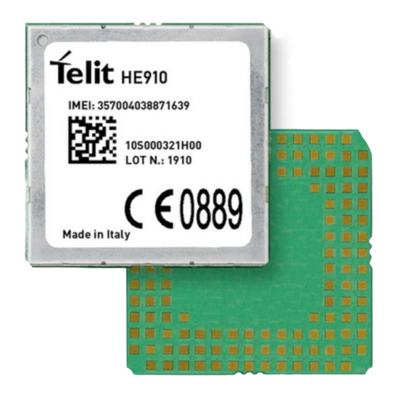
HE910 Hardware User Guide MOUNTING THE HE910 ON THE APPLICATION General The HE910 modules have been designed in order to be compliant with a standard lead- free SMT process. Module finishing & dimensions Pin B1 Bottom view Lead-free Alloy: Dimensions in mm... - Page 92 HE910 Hardware User Guide Figure 15-2 Module dimensions 1VV0300925 Rev. 32 Page 92 of 111 2019-11-25...
-
Page 93: Recommended Foot Print For The Application
VIEW Figure 15-3 Foot print In order to easily rework the HE910 is suggested to consider on the application a 1.5 mm placement inhibit area around the module. It is also suggested, as common rule for an SMT component, to avoid having a mechanical part of the application in direct contact with the module. -
Page 94: Stencil
HE910 Hardware User Guide Stencil Stencil’s apertures layout can be the same of the recommended footprint (1:1), we suggest a thickness of stencil foil ≥ 120 µm. PCB pad design Non solder mask defined (NSMD) type is recommended for the solder pads on the PCB. -
Page 95: Pcb Pad Dimensions
HE910 Hardware User Guide PCB pad dimensions The recommendation for the PCB pads dimensions are described in the following image (dimensions in mm) Figure 15-5 PCB pads dimensions 1VV0300925 Rev. 32 Page 95 of 111 2019-11-25... - Page 96 HE910 Hardware User Guide It is not recommended to place via or micro-via not covered by solder resist in an area of 0,3 mm around the pads unless it carries the same signal of the pad itself (see following figure).
-
Page 97: Solder Paste
15.7.1. HE910 Solder reflow Recommended solder reflow profile: Figure 15-7 HE910 Solder reflow Warning – The above solder reflow profile represents the typical SAC reflow limits and does not guarantee adequate adherence of the module to the customer application throughout the temperature range. - Page 98 HE910 Hardware User Guide Profile Feature Pb-Free Assembly Average ramp-up rate (T to T 3°C/second max Preheat – Temperature Min (Tsmin) 150°C – Temperature Max (Tsmax) 200°C – Time (min to max) (ts) 60-180 seconds Tsmax to TL – Ramp-up Rate 3°C/second max...
-
Page 99: Packing System (Tray)
Warning: The HE910 module withstands one reflow process only. Packing system (Tray) The HE910 modules are packaged on trays of 36 pieces each. These trays can be used in SMT processes for pick & place handling. 1VV0300925 Rev. 32 Page 99 of 111... - Page 100 HE910 Hardware User Guide Figure 15-8 Packing system 1 1VV0300925 Rev. 32 Page 100 of 111 2019-11-25...
- Page 101 HE910 Hardware User Guide Figure 15-9 Packing system 2 1VV0300925 Rev. 32 Page 101 of 111 2019-11-25...
-
Page 102: Packing System (Reel)
HE910 Hardware User Guide Packing System (Reel) The HE910 can be packaged on reels of 200 pieces each. See figure for module positioning into the carrier. Figure 15-10 Packing System 3 15.9.1. Carrier Tape Detail Figure 15-11 Carrier tape detail 1VV0300925 Rev. -
Page 103: Reel Detail
HE910 Hardware User Guide 15.9.2. Reel Detail Figure 15-12 Reel detail 1 Figure 15-13 Reel detail 2 1VV0300925 Rev. 32 Page 103 of 111 2019-11-25... -
Page 104: Packaging Detail
Figure 15-14 Packaging detail Moisture sensitivity The HE910 is a Moisture Sensitive Device level 3, in according with standard IPC/JEDEC J-STD-020, take care all the relatives requirements for using this kind of components. Moreover, the customer has to take care of the following conditions: a) Calculated shelf life in sealed bag: 12 months at <40°C and <90% relative humidity... -
Page 105: Safety Recommandations
HE910 Hardware User Guide SAFETY RECOMMANDATIONS READ CAREFULLY Be sure the use of this product is allowed in the country and in the environment required. The use of this product may be dangerous and has to be avoided in the following areas: •... -
Page 106: Fcc/Ic Regulatory Notices
The antenna should be installed and operated with minimum distance of 20 cm between the radiator and your body. Antenna gain must be below: Frequency band HE910, HE910-D HE910-NAR, HE910-NAD, HE910- GSM 850/FDD V 5.22 dBi 5.29 dBi PCS 1900/FDD II 3.31 dBi... - Page 107 L'antenne doit être installé de façon à garder une distance minimale de 20 centimètres entre la source de rayonnements et votre corps. Gain de l'antenne doit être ci-dessous: Frequency band HE910, HE910-D HE910-NAR, HE910-NAD, HE910- GSM 850/FDD V 5.22 dBi 5.29 dBi PCS 1900/FDD II 3.31 dBi...
-
Page 108: Anatel Approvals
HE910 Hardware User Guide ANATEL APPROVALS ANATEL Homologation #: 03120-11-02618 Applicable to the below listed variants: HE910 HE910-D HE910-GL HE910EUD HE910EUR HE910EUG 1VV0300925 Rev. 32 Page 108 of 111 2019-11-25... -
Page 109: Document History
USIF0 USIF1 names added to Main and AUX serial ports Updated IO logic levels Updated module’s mechanical drawing IO levels selection 1.8/1.2 removed (now only 1.8) Added HE910-GA and –D; added Conformity 2012-01-16 assessment chapter 2012-02-03 Chapter 5.1 updated 2012-02-07 Chapter 4.2 updated... - Page 110 HE910 Hardware User Guide 2012-06-14 Updated RTT&E info on HE910-NAG, NAR, 2012-06-15 Updated RTT&E info on HE910-NAG, NAR, NAD ; updated par 3.1; 2012-06-26 Pin P11 now reserved; updated par 3.1; par 4.2 2012-08-09 Updated par 9,1 5.3.2, 13.4, 3.1, 13.5 2013-04-29 Updated par 3.1, 5.1, 5.3.2, 6.4, 7, 9.1 ;...
- Page 111 Mod. 0805 2017-01 Rev.6...
Need help?
Do you have a question about the HE910 and is the answer not in the manual?
Questions and answers