Table of Contents
Advertisement
Quick Links
®
Description
The ISL54211EVAL1Z evaluation board is designed to
provide a quick and easy method for evaluating the
ISL54211 USB/Audio Switch IC.
The ISL54211 device is an unique IC. To use this evaluation
board properly requires a thorough knowledge of the
operation of the IC. Refer to the data sheet for an
understanding of the functions and features of the device.
Studying the device's truth-table along with its pinout
diagram on page 2 of the data sheet is the best way to get a
quick understanding of how the part works.
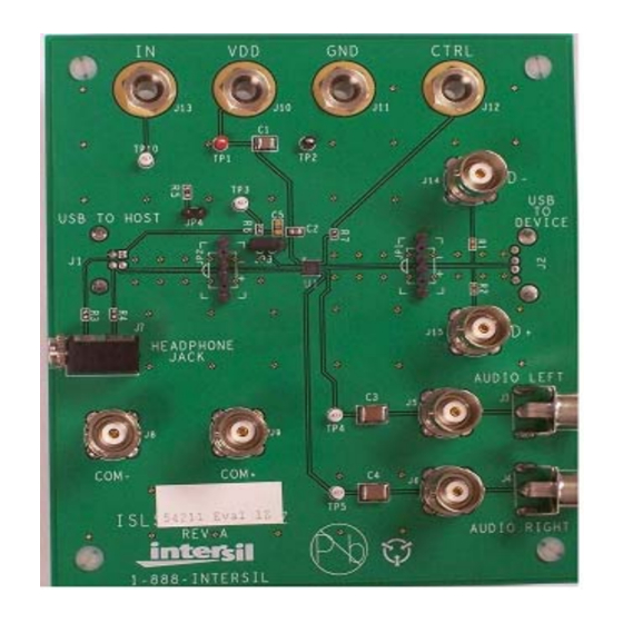
A picture of the main evaluation board is shown in Figure 1.
The ISL54211 TDFN IC is soldered onto the evaluation
board. It is located in the center of the board and is
designated as U1.
The ISL54211 IC has three modes of operation called Audio
mode, USB mode and Mute mode. The evaluation board
contains standard Audio and USB connectors to allow the
user to easily interface with the IC to evaluate its functions,
features, and performance in the these modes of operation.
For example, when the board is properly powered, a
headphone can be plugged into the headphone jack (J7) and
a stereo source, such as a MP3 player, can be connected at
the RCA connectors J3 (AUDIO LEFT) and J4 (AUDIO
RIGHT) to play music through the audio switches of the IC.
See Figure 2. You can then turn-off the audio source,
remove the headphones, configure the logic for USB
operation and then attach a USB cable from a computer to
the USB connector J1 (USB TO HOST). This will establish a
connection from the computer through the USB switches of
the IC to the USB device connected at the USB connector J2
(USB TO DEVICE), to send and receive data.
This application note will guide the user through the process
of configuring and using the evaluation board to evaluate the
ISL54211 device in both the Audio mode and the USB mode.
Features
• Standard USB Connectors
• RCA Audio Input Jacks and Headphone Speaker Jack
• Convenient Test Points and Connections for Test
Equipment
Application Note
1
CAUTION: These devices are sensitive to electrostatic discharge; follow proper IC Handling Procedures.
1-888-INTERSIL or 1-888-468-3774
Evaluation Board User's Manual
February 13, 2009
Picture of Evaluation Board (Top View)
FIGURE 1. ISL54211EVAL1Z EVALUATION BOARD
Board Architecture/Layout
Basic Layout of Evaluation Board
The basic layout of the main board is as follows: Refer to
Figure 1.
• Power and Ground connections are at the top of the board
(J10 and J11).
• Logic control connections are at the top of the board (J12
and J13).
• Audio Source Inputs are at the lower right side of the
board (J3 to J6). Audio outputs are at the lower left side of
the board (J7, J8, J9). Connector J7 is a standard
headphone jack for connecting a 32
• USB connection to an upstream host controller
(Computer) is made at connector J1, located on left under-
side of the board. USB connection to a downstream USB
device is made at connector J2, located on right under-
side of the board.
• Located in the center of the board is the ISL54211 IC (U1).
The evaluation board has a pin 1 dot, to show how the IC
should be oriented on to the evaluation board. The IC pin
1 indicator dot needs to be aligned with the evaluation
board pin 1 dot indicator.
|
Intersil (and design) is a registered trademark of Intersil Americas Inc.
Copyright Intersil Americas Inc. 2009. All Rights Reserved
All other trademarks mentioned are the property of their respective owners.
ISL54211EVAL1Z
AN1408.0
Ω
headphone.
Advertisement
Table of Contents

Related Manuals for Intersil ISL54211EVAL1Z


Summary of Contents for Intersil ISL54211EVAL1Z
- Page 1 CAUTION: These devices are sensitive to electrostatic discharge; follow proper IC Handling Procedures. 1-888-INTERSIL or 1-888-468-3774 Intersil (and design) is a registered trademark of Intersil Americas Inc. Copyright Intersil Americas Inc. 2009. All Rights Reserved All other trademarks mentioned are the property of their respective owners.
-
Page 2: Application Note
Application Note 1408 Power Supply forward biased and draw current as the voltage at the IN pin exceeds the VDD voltage. With V = 5.25V and VDD = The DC power supply connected at banana jacks J10 (VDD) μ 3.3V, this resistor will limit the current to around 2.76 A and and J11 (GND) provides power to the part. - Page 3 Application Note 1408 the D+ line of the J1 (USB To HOST) connector. These BNC Board Component Definitions connectors can be used to connect resistive loads and/or TABLE 1. BOARD COMPONENT DEFINITIONS test equipment to evaluate the performance of the IC. DESIGNATOR DESCRIPTION USB Connections...
- Page 4 AUDIO LEFT HEADPHONE JACK COM - COM + AUDIO RIGHT ISL54211EVAL1Z EVALUATION BOARD FIGURE 2. BASIC EVALUATION TEST SETUP BLOCK DIAGRAM Using The Board ( Audio Mode Operation Refer to Figure 2 1. Install headphone in the headphone jack, J7. No USB...
- Page 5 D-/D+ Differential Probe Connection - COM Side of Switch Intersil Corporation reserves the right to make changes in circuit design, software and/or specifications at any time without notice. Accordingly, the reader is cautioned to verify that the Application Note or Technical Brief is current before proceeding.
- Page 6 Board Schematic 10µF TP10 0.1µF CTRL MOUNT 4.3M COM1 DFN10 DEVICE COM2 HOST GENERIC PACK MOUNT AUDIO LEFT 100µF HEADPHONE JACK COM- AUDIO RIGHT 100µF COM+...
- Page 7 Мы молодая и активно развивающаяся компания в области поставок электронных компонентов. Мы поставляем электронные компоненты отечественного и импортного производства напрямую от производителей и с крупнейших складов мира. Благодаря сотрудничеству с мировыми поставщиками мы осуществляем комплексные и плановые поставки широчайшего спектра электронных компонентов.
Need help?
Do you have a question about the ISL54211EVAL1Z and is the answer not in the manual?
Questions and answers