Table of Contents
Advertisement
Quick Links
®
Description
The ISL54059EVAL1Z, ISL54060EVAL1Z,
ISL54061EVAL1Z, ISL54062EVAL1Z, ISL54063EVAL1Z
and ISL54064EVAL1Z evaluation board is designed to
provide a quick and easy method for evaluating the
ISL54059 through ISL54064 ICs.
The ISL54059 and ISL54062 ICs are a single supply Dual
Single-Pole Double Throw (SPDT) analog switches while the
ISL54060, ISL54061, ISL54063 and ISL54064 IC's are
single supply Dual Single-Pole Single Throw (SPST) analog
switches. All devices feature negative swing capability,
Ω
sub-
ON-resistance, and low power dissipation. The ICs
are designed for applications that require an analog switch
that may see voltages below ground at the switch terminals,
such as audio and video. The evaluation board is developed
to evaluate the ISL540XX ICs, integrating many features for
ease of use in examining the performance of the device
under various operating conditions. To help understand the
operation of the ISL540XX IC and the ISL540XXEVAL1Z
evaluation board, it is recommended to study the evaluation
board schematic found on page 4 of this document and the
datasheet for the IC under evaluation.
The ICs are analog switches that are capable of swinging
down to 6.5V below the positive supply rail. For example, if
the supply is at +1.8V, the switch terminal analog operating
range is from -4.3V to +1.8V. The ISL54062, ISL54063, and
ISL54064 also integrate Click and Pop Elimination Circuitry
to remove transient noises at the speaker during power
ON/OFF of an audio system. The evaluation board contains
standard RCA/BNC connectors and a single headphone jack
to allow the user to easily interface with the IC to evaluate its
functions, features, and performance.
This application note will guide the user through the process
of configuring and using the evaluation board to evaluate the
ISL540XX devices.
Key Features
• RCA Audio Input/Output Jacks, Stereo Headphone Output
Jack and BNC Connectors
• Convenient Test Points and Connections for Test
Equipment
• Click and Pop Elimination Circuitry (ISL54062, ISL54063,
and ISL54064)
• Manual or External Logic Input Control
ISL54059EVAL1Z Through ISL54064EVAL1Z
Application Note
1
CAUTION: These devices are sensitive to electrostatic discharge; follow proper IC Handling Procedures.
1-888-INTERSIL or 1-888-468-3774
Evaluation Board User's Manual
February 3, 2009
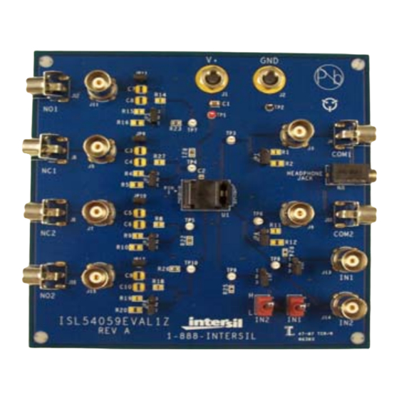
Picture of Evaluation Board (Top View)
FIGURE 1. ISL54059EVAL1Z THROUGH ISL54064EVAL1Z
EVALUATION BOARD
Board Architecture/Layout
Basic Layout of Evaluation Board
A picture of the evaluation board is located in Figure 1. The
ISL540XX IC is located inside socket U1 located at the
center of the evaluation board. The IC needs to be
orientated inside the socket such that the pin 1 indicator on
the IC is aligned with the pin 1 indicator dot inside the
socket. The evaluation board integrates the necessary
connections and components to interface with the ICs for
ease of operation.
Power Supply
The ISL540XX IC requires a supply voltage in the range of
+1.8V to +6.5V for proper operation. Banana jacks for V
(J1) and GND (J2) are located at the top of the board. The
evaluation board contains a 10µF bulk capacitor and a 0.1µF
high frequency decoupling capacitor at the supply lines.
Logic Control
The evaluation board contains two types of logic control to
the digital logic inputs of the IC available to the user. The
logic pins can be controlled either through manual or
external operation. The logic control pins are manually
toggled by the SPST switches mounted on the evaluation
board (S1-S2). When the switch is in the up position (H), the
associated logic pin is pulled to V
the switch is in the down position (L), the associated logic
pin is pulled to GND for logic LOW. For manual operation,
the jumpers JP6-JP7 need to be in the 2-3 position.
For external control via a function generator or switched
source, set the jumpers JP6-JP7 in the 1-2 position. This
by-passes the SPST switches and routes the logic control to
|
Intersil (and design) is a registered trademark of Intersil Americas Inc.
Copyright Intersil Americas Inc. 2009. All Rights Reserved
All other trademarks mentioned are the property of their respective owners.
AN1369.0
CC
for logic HIGH. When
CC
Advertisement
Table of Contents

Related Manuals for Intersil ISL54059EVAL1Z


Summary of Contents for Intersil ISL54059EVAL1Z
-
Page 1: Key Features
CAUTION: These devices are sensitive to electrostatic discharge; follow proper IC Handling Procedures. 1-888-INTERSIL or 1-888-468-3774 Intersil (and design) is a registered trademark of Intersil Americas Inc. Copyright Intersil Americas Inc. 2009. All Rights Reserved All other trademarks mentioned are the property of their respective owners. -
Page 2: Application Note
Application Note 1369 the BNC connectors J13-J14 located on the bottom right side Note: All switch terminals on the evaluation board have of the board. place holders that can have surface mounted components placed either in series with the switch path or shunted to Ω... - Page 3 (ISL54062 and ISL54064 only). Intersil Corporation reserves the right to make changes in circuit design, software and/or specifications at any time without notice. Accordingly, the reader is cautioned to verify that the Application Note or Technical Brief is current before proceeding.
- Page 4 ISL54059EVAL1Z Through ISL54064EVAL1Z Evaluation Board Schematic COM1 JP11 43 2 OPEN 10µF OPEN 0.1µF OPEN COM1 OPEN HEADPHONE JACK JP12 OPEN JP10 OPEN OPEN OPEN 4 3 2 COM2 COM2 4 3 2...
Need help?
Do you have a question about the ISL54059EVAL1Z and is the answer not in the manual?
Questions and answers