Table of Contents
Advertisement
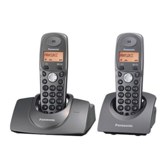
Telephone Equipment
KX-TG1105RUS
KX-TG1105RUT
KX-TG1106RUS
KX-TG1106RUT
KX-TGA110RUS
KX-TGA110RUT
Digital Cordless Phone
Silver Version
Titanium Black Version
(for Russia)
© 2006 Panasonic Communications Co., Ltd. All
rights
reserved.
distribution is a violation of law.
ORDER NO. KM40603006CE
Unauthorized
copying
and
Advertisement
Table of Contents
Troubleshooting

Related Manuals for Panasonic KX-TG1105RUS


Summary of Contents for Panasonic KX-TG1105RUS
- Page 1 ORDER NO. KM40603006CE Telephone Equipment KX-TG1105RUS KX-TG1105RUT KX-TG1106RUS KX-TG1106RUT KX-TGA110RUS KX-TGA110RUT Digital Cordless Phone Silver Version Titanium Black Version (for Russia) © 2006 Panasonic Communications Co., Ltd. All rights reserved. Unauthorized copying distribution is a violation of law.
-
Page 2: Table Of Contents
KX-TG1105RUS / KX-TG1105RUT / KX-TG1106RUS / KX-TG1106RUT / KX-TGA110RUS / KX-TGA110RUT Note: Because CONTENTS 4 is the extract from the Operating Instructions of this model, it is subject to change without notice. You can download and refer to the original Operating Instructions on TSN Server for further information. - Page 3 KX-TG1105RUS / KX-TG1105RUT / KX-TG1106RUS / KX-TG1106RUT / KX-TGA110RUS / KX-TGA110RUT 24.2. Introduction 31.3. Charger Unit 24.3. EEPROM contents 31.4. Accessories and Packing Materials 25 HOW TO REPLACE THE FLAT PACKAGE IC 31.5. Fixtures and Tools 25.1. PREPARATION 32 FOR SCHEMATIC DIAGRAM 25.2.
-
Page 4: About Lead Free Solder (Pbf: Pb Free)
KX-TG1105RUS / KX-TG1105RUT / KX-TG1106RUS / KX-TG1106RUT / KX-TGA110RUS / KX-TGA110RUT 1 ABOUT LEAD FREE SOLDER (PbF: Pb free) Note: In the information below, Pb, the symbol for lead in the periodic table of elements, will refer to standard solder or solder that contains lead. -
Page 5: How To Recognize That Pb Free Solder Is Used
KX-TG1105RUS / KX-TG1105RUT / KX-TG1106RUS / KX-TG1106RUT / KX-TGA110RUS / KX-TGA110RUT 1.2. How to recognize that Pb Free solder is used (Example: Handset P.C.B.) Marked (Component View) Note: The location of the “PbF” mark is subject to change without notice. -
Page 6: Operating Instructions
KX-TG1105RUS / KX-TG1105RUT / KX-TG1106RUS / KX-TG1106RUT / KX-TGA110RUS / KX-TGA110RUT 4 OPERATING INSTRUCTIONS 4.1. Battery 4.1.1. Battery Installation 4.1.2. Battery Charge... -
Page 7: Location Of Controls
KX-TG1105RUS / KX-TG1105RUT / KX-TG1106RUS / KX-TG1106RUT / KX-TGA110RUS / KX-TGA110RUT 4.2. Location of Controls 4.2.1. Base Unit 4.2.2. Handset 4.2.3. Charger (KX-TG1106 only) -
Page 8: Connections
KX-TG1105RUS / KX-TG1105RUT / KX-TG1106RUS / KX-TG1106RUT / KX-TGA110RUS / KX-TGA110RUT 4.3. Connections 4.3.1. Base Unit 4.3.2. Charger (KX-TG1106 only) Note: • • • • Never install telephone wiring during a lightning storm. • • • • Do not connect the AC adaptor to a ceiling-mounted AC outlet, as the weight of the adaptor may cause it to become disconnected. -
Page 9: Guide To Settings
KX-TG1105RUS / KX-TG1105RUT / KX-TG1106RUS / KX-TG1106RUT / KX-TGA110RUS / KX-TGA110RUT 4.4. Guide to Settings 4.4.1. Base Unit Cross Reference: For Service Hint (P.11) - Page 10 KX-TG1105RUS / KX-TG1105RUT / KX-TG1106RUS / KX-TG1106RUT / KX-TGA110RUS / KX-TGA110RUT 4.4.2. Handset Cross Reference: For Service Hint (P.11)
-
Page 11: For Service Hint
KX-TG1105RUS / KX-TG1105RUT / KX-TG1106RUS / KX-TG1106RUT / KX-TGA110RUS / KX-TGA110RUT 4.5. For Service Hint... -
Page 12: Disassembly Instructions
KX-TG1105RUS / KX-TG1105RUT / KX-TG1106RUS / KX-TG1106RUT / KX-TGA110RUS / KX-TGA110RUT 5 DISASSEMBLY INSTRUCTIONS 5.1. Base Unit Shown in Fig.- To Remove Remove Cabinet Cover Screws (2.6 × 12)..(A) × 2 Main P.C. Board Solders Main P.C. Board... -
Page 13: Handset
KX-TG1105RUS / KX-TG1105RUT / KX-TG1106RUS / KX-TG1106RUT / KX-TGA110RUS / KX-TGA110RUT 5.2. Handset Shown in Fig.- To Remove Remove Cabinet Cover Screws (2 × 8)..(B) × 2 Follow the procedure. Main P.C. Board Screw (2 × 8)....(C ) × 3 Tape and Solders Main P.C. -
Page 14: Charger Unit
KX-TG1105RUS / KX-TG1105RUT / KX-TG1106RUS / KX-TG1106RUT / KX-TGA110RUS / KX-TGA110RUT 5.3. Charger Unit Shown in Fig.- To Remove Remove Cabinet Cover Screws (2.6 × 14)..(D) × 2 Main P.C. Board Solders Main P.C. Board... -
Page 15: Assembly Instructions
KX-TG1105RUS / KX-TG1105RUT / KX-TG1106RUS / KX-TG1106RUT / KX-TGA110RUS / KX-TGA110RUT 6 ASSEMBLY INSTRUCTIONS 6.1. Warning When Constructing the Base Unit CHG terminal is properly fit in the cabinet. CHG terminal comes out of rib by pulling black lead wire when opening the cabinet and turning the PCB over. -
Page 16: How To Replace The Handset Lcd
KX-TG1105RUS / KX-TG1105RUT / KX-TG1106RUS / KX-TG1106RUT / KX-TGA110RUS / KX-TGA110RUT 6.2. How to Replace the Handset LCD... -
Page 17: Troubleshooting Guide
KX-TG1105RUS / KX-TG1105RUT / KX-TG1106RUS / KX-TG1106RUT / KX-TGA110RUS / KX-TGA110RUT 7 TROUBLESHOOTING GUIDE Flow Chart Cross Reference: Check Power (P.18) Bell Reception (P.22) Check Battery Charge (P.19) Check Link (P.20) Check Handset Transmission (P.22) Check Handset Reception (P.22) SIGNAL ROUTE (P.49) -
Page 18: Check Power
KX-TG1105RUS / KX-TG1105RUT / KX-TG1106RUS / KX-TG1106RUT / KX-TGA110RUS / KX-TGA110RUT 7.1. Check Power 7.1.1. Base Unit Is the AC Adaptor inserted into AC outlet? (Check AC Adaptor’s specification.) Cross Reference Note: Power Supply Circuit (P.44) BBIC is IC2. 7.1.2. -
Page 19: Check Battery Charge
KX-TG1105RUS / KX-TG1105RUT / KX-TG1106RUS / KX-TG1106RUT / KX-TGA110RUS / KX-TGA110RUT 7.2. Check Battery Charge 7.2.1. Base Unit Cross Reference: Power Supply Circuit (P.44) 7.2.2. Handset Cross Reference: Note: Check Power (P.18) BBIC is IC4. Charge Circuit (P.47) 7.2.3. Charger Unit Cross Reference: Power Supply Circuit (P.48) -
Page 20: Check Link
KX-TG1105RUS / KX-TG1105RUT / KX-TG1106RUS / KX-TG1106RUT / KX-TGA110RUS / KX-TGA110RUT 7.3. Check Link 7.3.1. Base Unit Cross Reference: Power Supply Circuit (P.44) Check Point (Base Unit) (P.23) Note: (*1) Refer to TROUBLESHOOTING BY SYMPTOM (BASE UNIT AND CHARGER UNIT) (P.23). - Page 21 KX-TG1105RUS / KX-TG1105RUT / KX-TG1106RUS / KX-TG1106RUT / KX-TGA110RUS / KX-TGA110RUT 7.3.2. Handset Cross Reference Power Supply Circuit/Reset Circuit (P.47) Check Point (Handset) (P.33) Note: (*1) Refer to TROUBLESHOOTING BY SYMPTOM (HANDSET) (P.33).
-
Page 22: Check Handset Transmission
KX-TG1105RUS / KX-TG1105RUT / KX-TG1106RUS / KX-TG1106RUT / KX-TGA110RUS / KX-TGA110RUT 7.4. Check Handset Transmission Cross Reference: SIGNAL ROUTE (P.49) 7.5. Check Handset Reception Cross Reference: HOW TO CHECK THE HANDSET SPEAKER (P.40). SIGNAL ROUTE (P.49) 7.6. Check Caller ID Cross Reference: SIGNAL ROUTE (P.49) -
Page 23: Troubleshooting By Symptom (Base Unit And Charger Unit)
KX-TG1105RUS / KX-TG1105RUT / KX-TG1106RUS / KX-TG1106RUT / KX-TGA110RUS / KX-TGA110RUT 8 TROUBLESHOOTING BY SYMPTOM (BASE UNIT AND CHARGER UNIT) If your unit has below symptoms, follow the instructions in remedy column. Remedies depend on whether you have DECT tester (*1) or not. - Page 24 KX-TG1105RUS / KX-TG1105RUT / KX-TG1106RUS / KX-TG1106RUT / KX-TGA110RUS / KX-TGA110RUT Items Adjustment Procedure Check or Point Replace Parts (D)* BBIC Confirmation 1. BBIC Confirmation (Execute the command “getchk”). IC2, X1, C32, 2. Confirm the returned checksum value. Connection of checksum value and program number is shown below.
- Page 25 KX-TG1105RUS / KX-TG1105RUT / KX-TG1106RUS / KX-TG1106RUT / KX-TGA110RUS / KX-TGA110RUT Items Adjustment Procedure Check or Point Replace Parts (J)* Frequency Offset Check Follow steps 1 to 3 of (H). IC2, IC3, L1, 4. Confirm that the frequency offset is -50kHz ~ +50kHz.
- Page 26 KX-TG1105RUS / KX-TG1105RUT / KX-TG1106RUS / KX-TG1106RUT / KX-TGA110RUS / KX-TGA110RUT Items Adjustment Procedure Check or Point Replace Parts (N)* Receive Audio Check 1. Configure the DECT tester (CMD60) as follows; IC2, C21, R31, and Adjustment C20, C11, <Setting> R18, R16, D3, •...
- Page 27 KX-TG1105RUS / KX-TG1105RUT / KX-TG1106RUS / KX-TG1106RUT / KX-TGA110RUS / KX-TGA110RUT Items Adjustment Procedure Check or Point Replace Parts (Q)* Audio Check 1. Link with Handset. 2. Set line voltage to 48V and line current to 40mA. 3. Input -45dBm/1kHz to MIC of Handset.
-
Page 28: The Setting Method Of Jig (Base Unit)
KX-TG1105RUS / KX-TG1105RUT / KX-TG1106RUS / KX-TG1106RUT / KX-TGA110RUS / KX-TGA110RUT 8.2. The Setting Method of JIG (Base Unit) 8.2.1. Preparation 8.2.1.1. Equipment Required • • • • DECT tester: Rohde & Schwarz, CMD 60 is recommended. • • • • Frequency counter: it must be precise to be able to measure 1Hz (precision; ±4ppm). - Page 29 KX-TG1105RUS / KX-TG1105RUT / KX-TG1106RUS / KX-TG1106RUT / KX-TGA110RUS / KX-TGA110RUT 8.2.2.2. PC Setting Note: • • • • “*****” varies depending on the country. • • • • See the table below for frequently used commands. Command name Function...
- Page 30 KX-TG1105RUS / KX-TG1105RUT / KX-TG1106RUS / KX-TG1106RUT / KX-TGA110RUS / KX-TGA110RUT...
- Page 31 KX-TG1105RUS / KX-TG1105RUT / KX-TG1106RUS / KX-TG1106RUT / KX-TGA110RUS / KX-TGA110RUT VBACK +2.65V...
-
Page 32: Adjustment Standard (Base Unit)
KX-TG1105RUS / KX-TG1105RUT / KX-TG1106RUS / KX-TG1106RUT / KX-TGA110RUS / KX-TGA110RUT 8.4. Check Point (Charger Unit) Items Adjustment Procedure Check or Point Replace Parts Charging Check 1. Connect Charge Contact 12Ω/2W resistor between charge+ and charge-. D1, R1, R2 2. Measure and confirm voltage across the resistor is 2.7V ± 0.2V. -
Page 33: Troubleshooting By Symptom (Handset)
KX-TG1105RUS / KX-TG1105RUT / KX-TG1106RUS / KX-TG1106RUT / KX-TGA110RUS / KX-TGA110RUT 9 TROUBLESHOOTING BY SYMPTOM (HANDSET) If your unit has below symptoms, follow the instructions in remedy column. Remedies depend on whether you have DECT tester (*1) or not. Note: (*1) A general repair is possible even if you don’t have the DECT tester because it is for confirming the levels, such as Acoustic... - Page 34 KX-TG1105RUS / KX-TG1105RUT / KX-TG1106RUS / KX-TG1106RUT / KX-TGA110RUS / KX-TGA110RUT Items Adjustment Procedure Check or Point Replace Parts (F)* Battery Monitor Check & 1. Apply 2.3V ± 0.005V between TP3(+) and TP4(-) with DC power. IC4, D2, L4, Adjustment (Important) L5, Q2, Q3, 2.
- Page 35 KX-TG1105RUS / KX-TG1105RUT / KX-TG1106RUS / KX-TG1106RUT / KX-TGA110RUS / KX-TGA110RUT Items Adjustment Procedure Check or Point Replace Parts (O)* Receive Audio Check TP15 1. Configure the DECT tester (CMD60) as follows; IC4, C67, C68, and Confirmation D7, D6, IC3, <Setting>...
-
Page 36: The Setting Method Of Jig (Handset)
KX-TG1105RUS / KX-TG1105RUT / KX-TG1106RUS / KX-TG1106RUT / KX-TGA110RUS / KX-TGA110RUT 9.2. The Setting Method of JIG (Handset) 9.2.1. Preparation 9.2.1.1. Equipment Required • • • • DECT tester: Rohde & Schwarz, CMD 60 is recommended. • • • • Frequency counter: it must be precise to be able to measure 1Hz (precision; ± 4ppm). - Page 37 KX-TG1105RUS / KX-TG1105RUT / KX-TG1106RUS / KX-TG1106RUT / KX-TGA110RUS / KX-TGA110RUT 9.2.2.2. PC Setting Note: • • • • “*****” varies depending on the country. • • • • See the table below for frequently used commands. Command name Function...
-
Page 38: Adjustment Standard (Handset)
KX-TG1105RUS / KX-TG1105RUT / KX-TG1106RUS / KX-TG1106RUT / KX-TGA110RUS / KX-TGA110RUT C64 C61 C56 C55 TP19 A201 C201 C203 C202 R113 C67 D7 C116 D102 R110 C108 R103 TP16 TP17 4.0V VBACK VBACK+ C204 C26 C28 C29 C8... -
Page 39: Things To Do After Replacing Ic
KX-TG1105RUS / KX-TG1105RUT / KX-TG1106RUS / KX-TG1106RUT / KX-TGA110RUS / KX-TGA110RUT 10 THINGS TO DO AFTER REPLACING IC Cautions: Since this page is common to each country, it may not apply to some models in your country. The contents below are the minimum adjustments required for operation. -
Page 40: Rf Specification
KX-TG1105RUS / KX-TG1105RUT / KX-TG1106RUS / KX-TG1106RUT / KX-TGA110RUS / KX-TGA110RUT 11 RF SPECIFICATION 11.1. Base Unit Item Value Refer to -. * TX Power More than 20 dBm ~ 25 dBm Check Point (Base Unit) (H) Modulation 340 kHz/div ~ 402 kHz/div... -
Page 41: Frequency Table (Mhz)
KX-TG1105RUS / KX-TG1105RUT / KX-TG1106RUS / KX-TG1106RUT / KX-TGA110RUS / KX-TGA110RUT 13 FREQUENCY TABLE (MHz) BASE UNIT HANDSET Channel No Transmit Frequency Receive Frequency Transmit Frequency Receive Frequency 1897.344 1897.344 1897.344 1897.344 1895.616 1895.616 1895.616 1895.616 1893.888 1893.888 1893.888 1893.888 1892.160... - Page 42 KX-TG1105RUS / KX-TG1105RUT / KX-TG1106RUS / KX-TG1106RUT / KX-TGA110RUS / KX-TGA110RUT...
-
Page 43: Block Diagram (Base Unit)
KX-TG1105RUS / KX-TG1105RUT / KX-TG1106RUS / KX-TG1106RUT / KX-TGA110RUS / KX-TGA110RUT 15 CIRCUIT OPERATION (BASE UNIT) 15.1. Outline Base Unit consists of the following ICs as shown in BLOCK DIAGRAM (BASE UNIT) (P.42). • • • • DECT BBIC (Base Band IC): IC2 −... -
Page 44: Power Supply Circuit
KX-TG1105RUS / KX-TG1105RUT / KX-TG1106RUS / KX-TG1106RUT / KX-TGA110RUS / KX-TGA110RUT 15.2. Power Supply Circuit The power is supplied to the DECT BBIC, RF Module, EEPROM, Relay Coil, LED and Charge Contact from AC Adaptor (+6V) as shown in Fig.101. The power supply is as follows:... -
Page 45: Telephone Line Interface
KX-TG1105RUS / KX-TG1105RUT / KX-TG1106RUS / KX-TG1106RUT / KX-TGA110RUS / KX-TGA110RUT 15.3. Telephone Line Interface <Function> • • • • Bell signal detection • • • • Clip signal detection • • • • ON/OFF hook circuit • • • • Audio circuits Bell &... -
Page 46: Block Diagram (Handset)
KX-TG1105RUS / KX-TG1105RUT / KX-TG1106RUS / KX-TG1106RUT / KX-TGA110RUS / KX-TGA110RUT 16 BLOCK DIAGRAM (HANDSET) Speech Burst RXDA Decoding Decoding EARPIECE TXDA Speech Burst Encoding Encoding Module RSSI ADPCM SYRI Codec Interface Analog SYEN Filter Front XTAL CHARGE CHARGE CHARGE 10.368... -
Page 47: Circuit Operation (Handset)
KX-TG1105RUS / KX-TG1105RUT / KX-TG1106RUS / KX-TG1106RUT / KX-TGA110RUS / KX-TGA110RUT 17 CIRCUIT OPERATION (HANDSET) 17.1. Outline Handset consists of the following ICs as shown in BLOCK DIAGRAM (HANDSET) (P.46). • • • • DECT BBIC (Base Band IC): IC4 −... -
Page 48: Circuit Operation (Charger Unit)
KX-TG1105RUS / KX-TG1105RUT / KX-TG1106RUS / KX-TG1106RUT / KX-TGA110RUS / KX-TGA110RUT 18 CIRCUIT OPERATION (CHARGER UNIT) 18.1. Power Supply Circuit The power supply is as shown. -
Page 49: Signal Route
KX-TG1105RUS / KX-TG1105RUT / KX-TG1106RUS / KX-TG1106RUT / KX-TGA110RUS / KX-TGA110RUT 19 SIGNAL ROUTE... -
Page 50: Cpu Data (Base Unit)
KX-TG1105RUS / KX-TG1105RUT / KX-TG1106RUS / KX-TG1106RUT / KX-TGA110RUS / KX-TGA110RUT 20 CPU DATA (BASE UNIT) 20.1. IC2 (BBIC) Description Hi-z Remarks PA_Driver_Amp PA_ON PA_OFF TX/RX SW RX_Data Data Data PLL_Strobe Latch Normal PLL_Data PLL_Clk TX_Data (NO USE) RF_System_Clk RESETQ... - Page 51 KX-TG1105RUS / KX-TG1105RUT / KX-TG1106RUS / KX-TG1106RUT / KX-TGA110RUS / KX-TGA110RUT Description Hi-z Remarks ANT1 ANT1_ON ANT1_OFF ANT2 ANT2_ON ANT2_OFF Note: I_PU; Internal Pull-Up, I_PD; Internal Pull-Down...
-
Page 52: Cpu Data (Handset)
KX-TG1105RUS / KX-TG1105RUT / KX-TG1106RUS / KX-TG1106RUT / KX-TGA110RUS / KX-TGA110RUT 21 CPU DATA (HANDSET) 21.1. IC4 (BBIC) Description Hi-z Remarks LCD_SEGMENT LCD_COMMON LCD_COMMON LCD_COMMON LCD_COMMON LCD_COMMON LCD_COMMON PA_SW PA ON PA OFF T/R SW Transmit Recieve RX_DATA SYEN SYDA... - Page 53 KX-TG1105RUS / KX-TG1105RUT / KX-TG1106RUS / KX-TG1106RUT / KX-TGA110RUS / KX-TGA110RUT Description Hi-z Remarks VDD for EEPROM I2DAT D.I/O I2CLK D.I/O MODE RINGER RINGER_ON RINGER_OFF VBACK/P0.7 LCD_SEGMENT LCD_SEGMENT LCD_SEGMENT LCD_SEGMENT LCD_SEGMENT VDDLI LCD_SEGMENT LCD_SEGMENT LCD_SEGMENT LCD_SEGMENT LCD_SEGMENT LCD_SEGMENT LCD_SEGMENT LCD_SEGMENT...
-
Page 54: Engineering Mode
KX-TG1105RUS / KX-TG1105RUT / KX-TG1106RUS / KX-TG1106RUT / KX-TGA110RUS / KX-TGA110RUT 22 ENGINEERING MODE 22.1. Base Unit Note: (*1) Refer to For Service Hint (P.11). - Page 55 KX-TG1105RUS / KX-TG1105RUT / KX-TG1106RUS / KX-TG1106RUT / KX-TGA110RUS / KX-TGA110RUT Note: *: When you enter the address, please refer to the table below. Desired Number (hex) Input Keys Desired Number (hex) Input Keys [R] + 0 [R] + 1...
-
Page 56: Handset
KX-TG1105RUS / KX-TG1105RUT / KX-TG1106RUS / KX-TG1106RUT / KX-TGA110RUS / KX-TGA110RUT 22.2. Handset Note: (*1) Refer to For Service Hint (P.11). - Page 57 KX-TG1105RUS / KX-TG1105RUT / KX-TG1106RUS / KX-TG1106RUT / KX-TGA110RUS / KX-TGA110RUT Note: *: When you enter the address, please refer to the table in Note: (P.55) of ENGINEERING MODE. ex.) Items (*4) Address Default Data New Data Possible Adjusted Possible Adjusted...
-
Page 58: Eeprom Layout (Base Unit)
KX-TG1105RUS / KX-TG1105RUT / KX-TG1106RUS / KX-TG1106RUT / KX-TGA110RUS / KX-TGA110RUT 23 EEPROM LAYOUT (BASE UNIT) 23.1. Scope The purpose of this section is to describe the layout of the EEPROM (IC1) for the KX-TG1105/1106 Base Unit. The EEPROM contains hardware, software, and user specific parameters. Some parameters are set during production of the base e.g. - Page 59 KX-TG1105RUS / KX-TG1105RUT / KX-TG1106RUS / KX-TG1106RUT / KX-TGA110RUS / KX-TGA110RUT Address Default Name Country Type Description Setting 09F2 HsRegInfo.EmcFlags Handset registration info - EMC flags 6..7: not used 0..5: handset 1..6 info, 1=known, 0=unknown 09F3 RingMode Ring mode. Modes used in KAMMA4 are 20h and 21h.
- Page 60 KX-TG1105RUS / KX-TG1105RUT / KX-TG1106RUS / KX-TG1106RUT / KX-TGA110RUS / KX-TGA110RUT Address Default Name Country Type Description Setting 0F4C Config BsUiTask configuration (LSB) Bits 1=enable 0=disable 0: FlashTime1Enabled, enabled 1: FlashTime2Enabled, enabled 2: FlashTime3Enabled, enabled 3: KeyClicksEnabled, disabled 4: ARSCarrierMenuEnabled, enabled...
-
Page 61: Eeprom Layout (Handset)
KX-TG1105RUS / KX-TG1105RUT / KX-TG1106RUS / KX-TG1106RUT / KX-TGA110RUS / KX-TGA110RUT 24 EEPROM LAYOUT (HANDSET) 24.1. Scope The purpose of this section is to describe the layout of the EEPROM (IC2) for the KX-TGA110 Handset. The EEPROM contains hardware, software, and user specific parameters. Some parameters are set during production of the handset e.g. - Page 62 KX-TG1105RUS / KX-TG1105RUT / KX-TG1106RUS / KX-TG1106RUT / KX-TGA110RUS / KX-TGA110RUT Address Default Name Country Type Description Setting 0196 LAL_4 Location area level for registration 4 0197 IPUI_LEN_4 IPUI length for registration 4 0198-01A4 FF .. FF IPUI_4 IPUI for registration 4...
- Page 63 KX-TG1105RUS / KX-TG1105RUT / KX-TG1106RUS / KX-TG1106RUT / KX-TGA110RUS / KX-TGA110RUT 24.3.4. Menu Configuration Address Default Name Country Type Description Setting 0F53 MenuConfig bit 0 - Registration menu on/off 1/0 bit 1 - Select base menu on/off 1/0 bit 2 - Internal ringer menu on/off 1/0...
-
Page 64: How To Replace The Flat Package Ic
KX-TG1105RUS / KX-TG1105RUT / KX-TG1106RUS / KX-TG1106RUT / KX-TGA110RUS / KX-TGA110RUT 25 HOW TO REPLACE THE FLAT PACKAGE IC Even if you do not have the special tools (for example, a spot heater) to remove the Flat IC, with some solder (large amount), a soldering iron and a cutter knife, you can easily remove the ICs that have more than 100 pins. -
Page 65: Flat Package Ic Installation Procedure
KX-TG1105RUS / KX-TG1105RUT / KX-TG1106RUS / KX-TG1106RUT / KX-TGA110RUS / KX-TGA110RUT 25.3. FLAT PACKAGE IC INSTALLATION PROCEDURE 1. Temporarily fix the FLAT PACKAGE IC, soldering the two marked pins. *Check the accuracy of the IC setting with the corresponding soldering foil. -
Page 66: Cabinet And Electrical Parts (Base Unit)
KX-TG1105RUS / KX-TG1105RUT / KX-TG1106RUS / KX-TG1106RUT / KX-TGA110RUS / KX-TGA110RUT 26 CABINET AND ELECTRICAL PARTS (BASE UNIT) -
Page 67: Cabinet And Electrical Parts (Handset)
27 CABINET AND ELECTRICAL PARTS (HANDSET) Note: (*1) The rechargeable Ni-MH battery P03P (HHR-4EPT or HHR-55AAAB) is available through sales route of Panasonic. (*2) This cable is fixed by welding. Refer to How to Replace the Handset LCD (P.16). (*3) Attach the spacer (No. 117) to the exact location described above. -
Page 68: Cabinet And Electrical Parts (Charger Unit)
KX-TG1105RUS / KX-TG1105RUT / KX-TG1106RUS / KX-TG1106RUT / KX-TGA110RUS / KX-TGA110RUT 28 CABINET AND ELECTRICAL PARTS (CHARGER UNIT) -
Page 69: Accessories And Packing Materials
KX-TG1105RUS / KX-TG1105RUT / KX-TG1106RUS / KX-TG1106RUT / KX-TGA110RUS / KX-TGA110RUT 29 ACCESSORIES AND PACKING MATERIALS 29.1. KX-TG1105RUS/RUT... -
Page 70: Kx-Tg1106Rus/Rut
KX-TG1105RUS / KX-TG1105RUT / KX-TG1106RUS / KX-TG1106RUT / KX-TGA110RUS / KX-TGA110RUT 29.2. KX-TG1106RUS/RUT... -
Page 71: Base Unit
KX-TG1105RUS / KX-TG1105RUT / KX-TG1106RUS / KX-TG1106RUT / KX-TGA110RUS / KX-TGA110RUT 30 TERMINAL GUIDE OF THE ICs, TRANSISTORS AND DIODES 30.1. Base Unit 30.2. Handset 30.3. Charger Unit... -
Page 72: Replacement Parts List
KX-TG1105RUS / KX-TG1105RUT / KX-TG1106RUS / KX-TG1106RUT / KX-TGA110RUS / KX-TGA110RUT 31 REPLACEMENT PARTS LIST 1. RTL (Retention Time Limited) Ref. Part No. Part Name & Description Remarks Note: PQJT10203Z CHARGE TERMINAL The marking (RTL) indicates that the Retention Time is... -
Page 73: Handset
KX-TG1105RUS / KX-TG1105RUT / KX-TG1106RUS / KX-TG1106RUT / KX-TGA110RUS / KX-TGA110RUT Ref. Part No. Part Name & Description Remarks Ref. Part No. Part Name & Description Remarks ERJ3GEYJ101 K0H1BB000018 SPECIAL SWITCH, TACTILE ERJ3GEYJ221 J0LF00000026 VARISTOR (SURGE ABSORBER) ERJ1WYJ330 H0D103500003 CRYSTAL OSCILLATOR... -
Page 74: Charger Unit
KX-TG1105RUS / KX-TG1105RUT / KX-TG1106RUS / KX-TG1106RUT / KX-TGA110RUS / KX-TGA110RUT Ref. Part No. Part Name & Description Remarks 31.3. Charger Unit PQLQR4D4R7K COIL 31.3.1. Cabinet and Electrical Parts G1C100MA0072 COIL G1C100MA0072 COIL Ref. Part No. Part Name & Description... -
Page 75: Fixtures And Tools
KX-TG1105RUS / KX-TG1105RUT / KX-TG1106RUS / KX-TG1106RUT / KX-TGA110RUS / KX-TGA110RUT Ref. Part No. Part Name & Description Remarks PQPP10084Z PROTECTION COVER (for Handset) PQPP10086Z PROTECTION COVER (for Charger Unit) PQPK15255Z GIFT BOX PQPD10667Z CUSHION 31.5. Fixtures and Tools Note: (*1) See The Setting Method of JIG (Base Unit) (P.28),... - Page 76 KX-TG1105RUS / KX-TG1105RUT / KX-TG1106RUS / KX-TG1106RUT / KX-TGA110RUS / KX-TGA110RUT Memo...
-
Page 77: For Schematic Diagram
KX-TG1105RUS / KX-TG1105RUT / KX-TG1106RUS / KX-TG1106RUT / KX-TGA110RUS / KX-TGA110RUT 32 FOR SCHEMATIC DIAGRAM 32.1. Base Unit (SCHEMATIC DIAGRAM (BASE UNIT)) Notes: 1. DC voltage measurements are taken with voltmeter from the negative voltage line. 2. This schematic diagram may be modified at any time with the development of new technology. -
Page 78: Schematic Diagram (Base Unit)
KX-TG1105RUS / KX-TG1105RUT / KX-TG1106RUS / KX-TG1106RUT / KX-TGA110RUS / KX-TGA110RUT 33 SCHEMATIC DIAGRAM (BASE UNIT) +60V DC ON-HOOK TP39 +10V DC OFF-HOOK LINE VOLTAGE 60V DC JMP1 0V ON-HOOK +0.7V DC OFF-HOOK TP45 100K TP40 JMP2 +2.65V JMP3 2.2K... - Page 79 KX-TG1105RUS / KX-TG1105RUT / KX-TG1106RUS / KX-TG1106RUT / KX-TGA110RUS / KX-TGA110RUT 0V ON-HOOK 0V ON-HOOK +3.9V DC OFF-HOOK +9.8V DC OFF-HOOK TP50 TP45 3.9K 100K D10P RX-AF A201 A202 TX-AF FREQ 10.368MHz +2.65V DC +2.65V TP187 TP10 +2.65V TP188 TX-DATA 33 PX.0...
-
Page 80: Schematic Diagram (Handset)
KX-TG1105RUS / KX-TG1105RUT / KX-TG1106RUS / KX-TG1106RUT / KX-TGA110RUS / KX-TGA110RUT 34 SCHEMATIC DIAGRAM (HANDSET) Frequency 324kHz 4.3V 4.1V DC 2.4V 4.0V 4.0V BATT 5.6n BATTERY+ R111 BATTERY- 3.3k CHARGE+ 2.65V CHARGE- EEPROM TP22 LCD Back Light LED VBACK+ 4.0V... - Page 81 KX-TG1105RUS / KX-TG1105RUT / KX-TG1106RUS / KX-TG1106RUT / KX-TGA110RUS / KX-TGA110RUT 4.0V TP101 TP102 R103 Q104 MIC+ 100n 100n 100n (10) (11) (12) 100n 2.2k (13) MIC- (14) (15) 100n (16) (17) (18) R26 NC (19) (20) R27 NC A201...
-
Page 82: Schematic Diagram (Charger Unit)
KX-TG1105RUS / KX-TG1105RUT / KX-TG1106RUS / KX-TG1106RUT / KX-TGA110RUS / KX-TGA110RUT 35 SCHEMATIC DIAGRAM (CHARGER UNIT) DC_PLUG Charge_plus Charge_minus pinL SCHEMATIC DIAGRAM (CHARGER UNIT) - Page 83 KX-TG1105RUS / KX-TG1105RUT / KX-TG1106RUS / KX-TG1106RUT / KX-TGA110RUS / KX-TGA110RUT...
- Page 84 KX-TG1105RUS / KX-TG1105RUT / KX-TG1106RUS / KX-TG1106RUT / KX-TGA110RUS / KX-TGA110RUT VBACK +2.65V...
- Page 85 KX-TG1105RUS / KX-TG1105RUT / KX-TG1106RUS / KX-TG1106RUT / KX-TGA110RUS / KX-TGA110RUT C64 C61 C56 C55 TP19 A201 C201 C203 C202 R113 C67 D7 C116 D102 R110 C108 R103 TP16 TP17 4.0V VBACK VBACK+ TP22 C204 C26 C28 C29 C8 MIC- MIC+...
- Page 86 KX-TG1105RUS / KX-TG1105RUT / KX-TG1106RUS / KX-TG1106RUT / KX-TGA110RUS / KX-TGA110RUT...
-
Page 87: Component View
KX-TG1105RUS / KX-TG1105RUT / KX-TG1106RUS / KX-TG1106RUT / KX-TGA110RUS / KX-TGA110RUT 38 CIRCUIT BOARD (CHARGER UNIT) 38.1. Component View PQUP11205Z CIRCUIT BOARD (CHARGER UNIT) Component View 38.2. Flow Solder Side View PQUP11205Z CIRCUIT BOARD (CHARGER UNIT) Flow Solder Side View...
Need help?
Do you have a question about the KX-TG1105RUS and is the answer not in the manual?
Questions and answers