Table of Contents
Advertisement
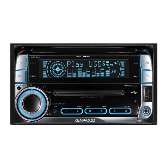
CD RECEIVER
DPX-MP3110
DPX-MP3110S
DPX-MP5110U
DPX-MP5110US
SERVICE MANUAL
SE
CONT
M.JOG
MENU
DISP
SCRL
FM+
AM-
SW
SE
CONT
M.JOG
MENU
DISP
SCRL
FM+
AM-
SW
Escutcheon
DC cord
(B07-3025-02)
(E30-6414-05)
DPX-MP3110
EXTERNAL MEDIA CONTROL
AUDIO
SET UP
ATT
SCAN
RDM
REP
DPX-MP5110U
EXTERNAL MEDIA CONTROL
AUDIO
SET UP
ATT
SCAN
RDM
REP
Screw set
(N99-1779-15)
© 2008-3 PRINTED IN JA PAN
B53-0624-00 ( N ) 243
DPX-MP3110
DPX-MP3110S
SRC
OFF
COL
S.A
Panel assy
MP3/WMA/AAC
DPX-MP3110 : (A64-4608-12)
VARIABLE
COLOR
DPX-MP3110S : (A64-4609-12)
AUX IN
M.RDM
DPX-MP5110U
DPX-MP5110US
SRC
OFF
COL
S.A
Panel assy
MP3/WMA/AAC
DPX-MP5110U : (A64-4458-12)
DPX-MP5110US : (A64-4462-12)
M.RDM
Remote controller assy (RC-547)
(A70-2085-05)
This product uses Lead Free solder.
RoHS
This product complies with the
Battery
(Not supplied)
directive for the European market.
Advertisement
Table of Contents

Related Manuals for Kenwood DPX-MP3110


Summary of Contents for Kenwood DPX-MP3110
- Page 1 © 2008-3 PRINTED IN JA PAN B53-0624-00 ( N ) 243 DPX-MP3110 DPX-MP3110S DPX-MP3110 CONT M.JOG MENU Panel assy DISP MP3/WMA/AAC DPX-MP3110 : (A64-4608-12) VARIABLE SCRL COLOR DPX-MP3110S : (A64-4609-12) EXTERNAL MEDIA CONTROL AUX IN AUDIO SET UP SCAN M.RDM...
- Page 2 ILLUMI+B ILLUMI+B P. ON ILLUMI Q200-202 Q45,46 SYSTEM INDICATOR S-MOTOR+B S-MOTOR+B CONTROLLER BACK AUX IN SW14V & DRIVER LIGHT RESET ROTARY ENCODER LCD DRIVER 4-DIRECTION & CENTER PUSH S2-15 IC2,5 D220-222, SW5V PAN5V REMOTE & ILLUMI MATRIX SW5V BUFFER DPX-MP3110...
- Page 3 (X34- ) IC450 C170,D170, R170 POWER SP-OUT BU5V PHONE DME1 PHONE FRONT L/R Q180 MECHA REAR L/R BU5V DIMMER DIMMER IC200 Q122 AUDIO WH340 800mV ACC-DET ACC-DET PROCESSOR Q400-403 J400 DC-CN A340 IC201 PRE-OUT IC470 MUTE FRONT/ Q120 LEVEL SW REAR, NF PHONE SW5V...
-
Page 4: Block Diagram
DPX-MP3110/MP3110S DPX-MP5110U/MP5110US BLOCK DIAGRAM MOTHER CD PLAYER UNIT (X32-6130-00) BOARD (X34- ) DPU1 SRAMSTB SRAMSTB SIGNAL A,B,C,E,F BUCK BUCK PIO0 PIO0 MRST MRST RF AMP BSIF ST REQ BSIF ST REQ VREF SERVO BSIF GATE BSIF GATE PROCESSOR BSIF DATA... - Page 5 DPX-MP3110/MP3110S DPX-MP5110U/MP5110US COMPONENTS DESCRIPTION ● ELECTRIC UNIT (X34-573x-xx) Ref. No. Application / Function Operation / Condition / Compatibility IC10 AUD8V REF Power Supply Outputs 1.27V. IC70 USB5V Switching regulator. IC200 Audio Processor Sound enhancer. IC201 Level SW Sound enhancer level control.
- Page 6 DPX-MP3110/MP3110S DPX-MP5110U/MP5110US COMPONENTS DESCRIPTION Ref. No. Application / Function Operation / Condition / Compatibility Q690 SRAM-STBY (MP3110/S) CD mechanism standby SW. Q690 SOC Stop (MP5110U/US) X17 unit standby SW. ● SWITCH UNIT (X16-620x-xx) Ref. No. Application / Function Operation / Condition / Compatibility LCD Driver ED1 Driver.
- Page 7 DPX-MP3110/MP3110S DPX-MP5110U/MP5110US COMPONENTS DESCRIPTION Ref. No. Application / Function Operation / Condition / Compatibility D3.3V REG. Power supply for digital 3.3V. IC11 BU1.5V REG. Power supply for back-up 1.5V. APC (Auto Power Control) Drives LD (Laser Diode). Inverter Inverts ZDET signal.
- Page 8 DPX-MP3110/MP3110S DPX-MP5110U/MP5110US MICROCOMPUTER’S TERMINAL DESCRIPTION Truth Value Pin No. Pin Name Application Processing / Operation / Description Table CD MRST Zipang (CD mechanism μ-com) reset (MP3110/S) H: CD playing, L: Reset SOC SRST Bolero reset (MP5110U/US) H: Normal, L: Reset Servo &...
- Page 9 DPX-MP3110/MP3110S DPX-MP5110U/MP5110US MICROCOMPUTER’S TERMINAL DESCRIPTION Truth Value Pin No. Pin Name Application Processing / Operation / Description Table TAP SMOTOR2 Not used TAP METAL Not used TAP EQ MUTE Not used TAP FWD REV Not used TAP DOLBY B Not used...
- Page 10 DPX-MP3110/MP3110S DPX-MP5110U/MP5110US MICROCOMPUTER’S TERMINAL DESCRIPTION Truth Value Pin No. Pin Name Application Processing / Operation / Description Table ILLUMI DET Dimmer illumination detection L: ON, H: OFF LINE MUTE Line mute detection TEL mute: Below 1V, NAVI mute: Over 2.5V...
-
Page 11: Test Mode
DPX-MP3110/MP3110S DPX-MP5110U/MP5110US TEST MODE ■ Example Description of display Description Disc Eject times display. MAX 65535 (times) CD=EJT Disc Eject times display While disc EJECT times is displayed, press and hold for 2 seconds or longer to clear disc EJECT times. (This is to clear only the display ■5... - Page 12 DPX-MP3110/MP3110S DPX-MP5110U/MP5110US TEST MODE Description Default values Spectrum analyzer “Peak Hold” GUID Variable LED White LED is used in all of three systems (i.e, Backlight, and Around key and knob) (R=9, G=9, B=9) S·E (Eala) ■ Special displays when all lights are on in standby source...
- Page 13 DPX-MP3110/MP3110S DPX-MP5110U/MP5110US TEST MODE Description of display Description ROM data transfer ■AM Audio data initialization Audio setting value is re-set to the Test mode default value. No forced Power OFF – – – Power is turned OFF forcibly because the Security Code is not yet written.
- Page 14 DPX-MP3110/MP3110S DPX-MP5110U/MP5110US TEST MODE ■ Test mode specifi cations in Tuner source Error is found in front-end, etc. if indications below is displayed while in tuner source. Status Description of display Description E2PROM in the front-end has its default values (Uncertain values) Front-end E2PROM data error as they are.
- Page 15 DPX-MP3110/MP3110S DPX-MP5110U/MP5110US TEST MODE ■ Test mode specifi cations in CD source Display mode default: P-Time • Procedure in CD-DA media (KTD-02A) Description of display Description Every time pressed, jumps to the track shown below. No.9 → No.15 → No.10 → No.11 → No.12 → No.13 → No.22 →...
- Page 16 DPX-MP3110/MP3110S DPX-MP5110U/MP5110US TEST MODE Procedure Item Procedure Description Fader Adjust to 3 steps of R15 ↔ 0 ↔ F15. (Default value: 0) Balance Adjust to 3 steps of L15 ↔ 0 ↔ R15. (Default value: 0) [VOL] knob and Bass Level...
- Page 17 DPX-MP3110/MP3110S DPX-MP5110U/MP5110US TEST MODE ■ Initialization of Audio related setting values Procedure Display Note Press [ ] key briefl y in the standby source “AUD INIT” Audio setting value is re-set to default value in the Test mode. ■ Preout switching...
- Page 18 DPX-MP3110/MP3110S DPX-MP5110U/MP5110US TEST MODE ■ Clearing DC error detection information (E2PROM data clearing) Procedure Note While pressing and holding [3] key and [6] key, reset-start. To enter DC error display mode. While “– – – –” is displayed, power can be ON for 30 minutes. This mode is cancelled by resetting. (The last screen will not be retained.)
- Page 19 DPX-MP3110/MP3110S DPX-MP5110U/MP5110US TEST MODE ■ ROM data transfer process Procedure Display Description While pressing and holding [1] key All lights ON. and [3] keys, reset-start Press [M.JOG] key briefl y (MENU) Menu mode Front-end → Mother. Data transfer processing. Press [ ] key or [ ] key briefl...
- Page 20 DPX-MP3110/MP3110S DPX-MP5110U/MP5110US ROM DATA TRANSFER PROCESSES ■ Operation procedure When replacing front-end (A1) of mother unit (X34-), or when adding or replacing ROM correction (program correction Operation procedure is different depending on the condi- with ROM IC (IC10)), the following activities are required.
- Page 21 DPX-MP3110/MP3110S DPX-MP5110U/MP5110US ROM DATA TRANSFER PROCESSES Turn power on. Install new front-end (A1). Press and hold the [1] and [3] keys and press reset button. No ROM correction or other data status. (Enter the system in the test mode.) Press [B.BOOST] key. (ROM data System enters data trans- fer mode.)
- Page 22 DPX-MP3110/MP3110S DPX-MP5110U/MP5110US ROM DATA TRANSFER PROCESSES 4. In case of applying a new ROM correction when front- Turn power on. end (A1) is replaced (There is ROM correction data.) Press and hold the [1] and [3] keys, press reset button. (Enter 5.
- Page 23 DPX-MP3110/MP3110S DPX-MP5110U/MP5110US ROM DATA TRANSFER PROCESSES Press key. (Exit ROM data transfer mode.) Turn power on. Turn power off. Press and hold the [1] and [3] keys press reset button. (Enter the system in the test mode.) Remove front-end (A1).
- Page 24 DPX-MP3110/MP3110S DPX-MP5110U/MP5110US PC BOARD (COMPONENT SIDE VIEW) ELECTRIC UNIT X34-573x-xx (J76-0493-02) W807 W813 W809 IC450 11 12 8 4 3 J400 9 10 6 R402 R403 J420 W808 R400 R401 C423 W812 WH340 R431 R457 Q402 Q403 W806 C461 Q400 Q401...
- Page 25 DPX-MP3110/MP3110S DPX-MP5110U/MP5110US WH500 W824 X34-573x-xx W829 C181 D170 C122 Ref. No. Address W826 C170 IC10 W832 W825 IC70 W821 W833 W819 IC200 IC201 R144 R151 IC320 R152 R142 IC450 W827 IC470 IC500 D123 IC502 R132 W828 IC690 Q122 IC691 D121...
- Page 26 DPX-MP3110/MP3110S DPX-MP5110U/MP5110US PC BOARD (FOIL SIDE VIEW) ELECTRIC UNIT X34-573x-xx (J76-0493-02) R130 R133 Q150 R479 R472 R473 C515 IC501...
- Page 27 DPX-MP3110/MP3110S DPX-MP5110U/MP5110US X34-573x-xx Ref. No. Address IC501 R340 Q141 Q142 Q143 Q150 Q340 Q341 Q550 Q551 R321 R320 R434 R433 IC501 Refer to the schematic diagram for the values of resistors and capacitors.
- Page 28 DPX-MP3110/MP3110S DPX-MP5110U/MP5110US PC BOARD (COMPONENT SIDE VIEW) PROCESSOR UNIT X17-2000-00 A/2 (J76-0492-02) *DPX-MP5110U/US only WH770 R725 IC751 R733 BOOT R765 R766 R778 R760 R701 R743 R781 Q703 C775 R710 Q702 IC771 Q701 C776 CN771 X17-2000-00 Ref. No. Address IC751 IC771...
- Page 29 DPX-MP3110/MP3110S DPX-MP5110U/MP5110US PC BOARD (FOIL SIDE VIEW) PROCESSOR UNIT X17-2000-00 A/2 (J76-0492-02) *DPX-MP5110U/US only C770 X701 D771 D770 R720 C774 R727 C710 L770 C711 R732 IC750 IC770 R730 R729 C772 R734 R731 R716 R736 R735 R751 R715 IC700 R717 6 10...
- Page 30 DPX-MP3110/MP3110S DPX-MP5110U/MP5110US PC BOARD (COMPONENT SIDE VIEW) SWITCH UNIT X16-620x-xx (J76-0490-12) D220 J100 D221 D201 D222 X16-620x-xx Ref. No. Address D211 D200 D224 Refer to the schematic diagram for the values of resistors and capacitors.
- Page 31 DPX-MP3110/MP3110S DPX-MP5110U/MP5110US PC BOARD (FOIL SIDE VIEW) SWITCH UNIT X16-620x-xx (J76-0490-12) CN100 R100 R101 D101 D100 R208 Q222 R233 R203 R232 R231 R205 R207 R229 Q221 Q220 R223 R225 R224 X16-620x-xx Ref. No. Address Q200 Q201 Q202 Q210 Q211 R211...
- Page 32 DPX-MP3110/MP3110S DPX-MP5110U/MP5110US PC BOARD (COMPONENT SIDE VIEW) CD PLAYER UNIT X32-6130-00 (J76-0495-12) R261 R216 C104 R281 X32-6130-00 Ref. No. Address Refer to the schematic diagram for the values of resistors and capacitors.
- Page 33 DPX-MP3110/MP3110S DPX-MP5110U/MP5110US PC BOARD (FOIL SIDE VIEW) SGND S7.5V CD PLAYER UNIT LO/EJ DRVMUTE MOTOR X32-6130-00 (J76-0495-12) SPDL+ R288 LOE-SW 8-SW SRAM MRST PIO0 AMUTE SLD- SLD+ LOAD A.GND EJECT SPDL- BUCK R240 R289 BU1.5V C101 R241 R246 R231 D1.5V...
- Page 34 DPX-MP3110/MP3110S DPX-MP5110U/MP5110US ELECTRIC UNIT (X34-573x-xx) WH340 AGND ∗ A340 Q400-403 PRE OUT MUTE SW FRONT-END R404 R405 Q400 Q401 C342 C343 0.01 C340 0.01 0.01 TUNGND Q404 TUNGND TP521 C341 TP527 TP535 D402 0.01 R341 Q340 Q341 ∗ TP523 R340...
- Page 35 DPX-MP3110/MP3110S DPX-MP5110U/MP5110US PRE OUT ∗ J400 J420 Q404,405 AGND TP565 PRE OUT MUTE DRIVER IC2+B R405 R406 R407 R212 5L I/F 7.5K Q401 Q402 Q403 R211 TP577 TP566 7.5K R431 AGND Q405 C423 0.01 IC200 D425 D428 D403 D421 D423...
- Page 36 DPX-MP3110/MP3110S DPX-MP5110U/MP5110US R479 IC2+B TP586 AGND AGND IC200 AUDIO PROCESSOR 8.0V MUTE MUTE MUTE 12 13 14 18 14 18 4.0V BU5V BU5V TP58 UCOM 5V UCOM 5V DGND DGND SYSTEM u-COM IC501 RESET CONTROL 5.0V C515 R202 R203 R204 0.01...
- Page 37 DPX-MP3110/MP3110S DPX-MP5110U/MP5110US TP636 F1 10A (F52-0023-05) to DC CORD TP637 TP633 IC10 AUD8V REF AGND POWER SUPPLY IC10 TP632 TP631 1.3V 13.7V MUTE AGND BU5V TP587 L501 L500 4.7uH TP591 Q20,21 BU5V AVR BU5V BU5V DGND PON5V TP635 NOT USED...
- Page 38 ∗ CAUTION : For continued safety, re place safe ty critical com po nents only with manu- DPX-MP3110/MP3110S/MP5110U/MP5110US (1/3) facturer’s rec om mend ed parts (refer to parts list). Indicates safety critical com po nents. To reduce the risk of electric shock, leakage- cur rent or re sis tance mea sure ments shall be carried out (ex posed parts are ac cept ably in su lat ed from the supply cir cuit) be fore the ap pli ance is returned to the customer.
- Page 39 DPX-MP3110/MP3110S DPX-MP5110U/MP5110US to SWITCH UNIT (X16-CN100) IC700 : 92CD28AFG6VD1 IC750 IC751 (X17-200x-xx) IC770 : STMPS2151STR WH770 R703, UNIT IC771 : R1114N331B-TR MODEL NAME R759 R760 IC800 USB IF DPX-MP5110U/US 0-00 TP770 DPX-U60MD Q701 : DTA114YUA 0-01 Q702,704,705 DVCC BU3.3V 0-02 3.3K...
- Page 40 VOUT a high impedance volt me ter. Val ues may vary slight ly due to vari a tions between in di vid u al in stru ments or/ and units. DPX-MP3110/MP3110S/MP5110U/MP5110US (2/3) SIGNAL LINE GND LINE B LINE 690) X17-2000-00 (2/2)
- Page 41 DPX-MP3110/MP3110S DPX-MP5110U/MP5110US SWITCH UNIT (X16-620x-xx) 4.7K TEST 680P VLCD4 1.7V VLCD3 3.4V VLCD VLCD2 5.2V CONTROLLER VLCD1 7.0V LCD DRIVER VLCD0 8.7V VLCD 5.0V REMOTE CONTROL RECEIV KEY M P4 OE P2 5.0V GND2 PON P1 VOUT GND1 CP2 1K SW5V 7.0V...
- Page 42 DPX-MP3110/MP3110S DPX-MP5110U/MP5110US (SEGMENT) KEY ILL ROL RECEIVER GND2 GND1 2.2M Q220-222 5.0V DRIVER Q220 Q221 Q222 0.01 ( COMMON ) IC2 OUTPUT BUFFER AMP BACK LIGHT ENCODER Q210-212 DRIVER Q201 Q202 Q210 Q211 Q212 ∗ R102 (X16-620x-xx) IC1 : LC75808W-E : 02DZ9.1F-Z...
- Page 43 DPX-MP3110/MP3110S DPX-MP5110U/MP5110US DPX-MP3110/MP3110S/MP5110U/MP5110US (3/3) CAUTION : For continued safety, re place safe ty critical com po nents only with manufacturer’s rec om mend ed parts (refer to parts list). Indicates safety critical com po nents. To reduce the risk of electric...
- Page 44 DPX-MP3110/MP3110S DPX-MP5110U/MP5110US CD PLAYER UNIT (X32-6130-00) 4CH BTL DRIVER 1.5V POWVCC1 TP203 POWGND1 TP31 SLIN R207 TP204 SPDL- VO1- LDIN TP32 BIASSW TP33 SPDL+ VO1+ C20 33P TP34 TP28 EJECT R20 180K VO2- TP55 TP26 R27 9.1K LOAD VO2+ TP54...
- Page 45 DPX-MP3110/MP3110S DPX-MP5110U/MP5110US 3.3V R233 R287 16.934MHz TP44 FCS+ 3300P TP47 TRK- TP46 1.9V TRK+ 2200P TP45 DPU1 FCS- (X92- ) 0.033 0.033 TP84 TP71 2.1V TP40 OPTICAL TP41 PICKUP 87.7kHz TP72 1.8V 2.5V 16.934MHz 1.5V 2.1V DVSS3 1 1.7V TP42 88.8kHz...
- Page 46 DPX-MP3110/MP3110S DPX-MP5110U/MP5110US EXPLODED VIEW (CD MECHANISM) DPU1 DFPC1 (X32) : N09-4460-15 φ M1.6x6.0 : N09-6317-05 M1.7x2.5 : N09-6004-15 M2x2 : N09-6007-15 2x5(BLK) : N09-6051-15 φ 1.6 WASHER : N19-2163-04 M2x2 : N39-2020-48 2x3.5 : N09-6108-15 φ : N09-6155-15 φ Parts with the exploded numbers larger than 700 are not supplied.
- Page 47 φ3x5 N83-3008-48 φ3x8 N83-3020-48 φ3x20 N80-3010-48 φ3x10 N82-2608-48 φ2.6x8 N84-3005-43 φ3x5 DME1 DPX-MP5110U/US only FC1: DPX-MP3110/S FC3: DPX-MP5110U/US (X17-) (X34-) WH340 (X34-) (X34-) WH500 A340 (X34-) (X34-) IC70 248 (X34- : ELECTRIC UNIT) ∗ Replacement part only for DPX-MP5110U/US On bottom of IC70 there is a soldering part.
- Page 48 DPX-MP3110/MP3110S DPX-MP5110U/MP5110US EXPLODED VIEW (PANEL) Size AA battery (Not supplied) N78-2660-48 φ2.6x6 N80-2005-48 φ2x5 N80-2008-48 φ2x8 (X16-) (X16-) (X16-) (X16-) (X16-) (X16-) (X16-) (X16-) Parts with the exploded numbers larger than 700 are not supplied.
-
Page 49: Parts List
CHIP C 2.2UF R234 RK73GB2A473J CHIP R J 1/10W C50,51 CC73GCH1H101J CHIP C 100PF C100 CK73GB1C104K CHIP C 0.10UF M1M4 S70-0947-05 TACT SWITCH M1 : DPX-MP5110U M4 : DPX-MP5110US M5 : DPX-MP3110 M6 : DPX-MP3110S Indicates safety critical com po nents. - Page 50 CHIP R J 1/10W M1M4 CK73GB1H103K CHIP C 0.010UF K R720 RK73GB2A223J CHIP R J 1/10W M1M4 C47,48 CK73GB1H333K CHIP C 0.033UF K M1 : DPX-MP5110U M4 : DPX-MP5110US M5 : DPX-MP3110 M6 : DPX-MP3110S Indicates safety critical com po nents.
- Page 51 CK73GB1A105K CHIP C 1.0UF R231 RK73GB2A473J CHIP R J 1/10W C142 CD04AS1H3R3M ELECTRO 3.3UF 50WV M1M4 C142 CD04AT1H3R3M ELECTRO 3.3UF 50WV M5M6 M1 : DPX-MP5110U M4 : DPX-MP5110US M5 : DPX-MP3110 M6 : DPX-MP3110S Indicates safety critical com po nents.
- Page 52 CK73GB1H102K CHIP C 1000PF R131 RK73GB2A473J CHIP R J 1/10W C515 CK73GB1H103K CHIP C 0.010UF K R132 RK73FB2B683J CHIP R J 1/8W M1 : DPX-MP5110U M4 : DPX-MP5110US M5 : DPX-MP3110 M6 : DPX-MP3110S Indicates safety critical com po nents.
- Page 53 CHIP R J 1/10W M1M4 R457 RK73GB2A333J CHIP R J 1/10W R806 RK73EB2E000J CHIP R J 1/4W R459,460 RK73GB2A000J CHIP R J 1/10W M1 : DPX-MP5110U M4 : DPX-MP5110US M5 : DPX-MP3110 M6 : DPX-MP3110S Indicates safety critical com po nents.
- Page 54 2SC4081 TRANSISTOR G01-3077-14 EXTENSION SPRING Q140 DTC114YUA DIGITAL TRANSISTOR G02-1399-14 FLAT SPRING Q141 DTA114EUA DIGITAL TRANSISTOR G02-1547-14 FLAT SPRING Q142 2SA1576A TRANSISTOR M1 : DPX-MP5110U M4 : DPX-MP5110US M5 : DPX-MP3110 M6 : DPX-MP3110S Indicates safety critical com po nents.
- Page 55 N09-6108-15 TAPTITE SCREW (M2X3.5) N09-6155-15 SEMS (TAPTITE SCREW) (PT2X6) T42-1066-14 DC MOTOR (SPINDLE) T42-1067-14 DC MOTOR (LOADING/SLED) DPU1 X93-2130-01 OPTICAL PICKUP ASSY M1 : DPX-MP5110U M4 : DPX-MP5110US M5 : DPX-MP3110 M6 : DPX-MP3110S Indicates safety critical com po nents.
-
Page 56: Specifications
Weight AAC decode .......... AAC-LC “.m4a” fi les DPX-MP5110U/US ..........1.60 kg DPX-MP3110/S ............1.55 kg KENWOOD follows a policy of continuous advancements in development. For this reason specifications may be changed without notice. DANGER: Please do not look at the laser beam directly during...
Need help?
Do you have a question about the DPX-MP3110 and is the answer not in the manual?
Questions and answers