Telit Wireless Solutions GE866-QUAD Hardware User's Manual
Hide thumbs
Also See for GE866-QUAD:
- Hardware user's manual (82 pages) ,
- Design manual (32 pages) ,
- User manual (79 pages)
Table of Contents
Advertisement
Quick Links
Advertisement
Table of Contents

Related Manuals for Telit Wireless Solutions GE866-QUAD


Summary of Contents for Telit Wireless Solutions GE866-QUAD
- Page 1 GE866-QUAD Hardware User Guide 1VV0301051 Rev. 2 – 2014-04-07...
- Page 2 GE866-DUAL Hardware User Guide 1VV0301051 Rev. 2 – 2014-04-07 APPLICABILITY TABLE PRODUCT GE866-QUAD Reproduction forbidden without written authorization from Telit Communications S.p.A. - All Rights Reserved. Page 2 of 82 Mod. 0805 2011-07 Rev.2...
- Page 3 GE866-DUAL Hardware User Guide 1VV0301051 Rev. 2 – 2014-04-07 SPECIFICATIONS SUBJECT TO CHANGE WITHOUT NOTICE Notice While reasonable efforts have been made to assure the accuracy of this document, Telit assumes no liability resulting from any inaccuracies or omissions in this document, or from use of the information obtained herein.
- Page 4 GE866-DUAL Hardware User Guide 1VV0301051 Rev. 2 – 2014-04-07 Usage and Disclosure Restrictions License Agreements The software described in this document is the property of Telit and its licensors. It is furnished by express license agreement only and may be used only in accordance with the terms of such an agreement.
-
Page 5: Table Of Contents
6.3.3. Power Supply PCB layout Guidelines ......32 Antenna ............. 34 7.1. GSM Antenna Requirements ......... 34 7.1.1. GE866-QUAD Antenna – PCB line Guidelines ....34 7.2. PCB Design Guidelines ........37 7.2.1. Transmission line design ........37 7.2.2. Transmission line measurements ......38 Reproduction forbidden without written authorization from Telit Communications S.p.A. - Page 6 GE866-DUAL Hardware User Guide 1VV0301051 Rev. 2 – 2014-04-07 7.3. GSM Antenna - installation Guidelines ....39 Logic levels specifications ......... 40 8.1. Reset signal ..........41 Serial Ports ..........43 9.1. Modem Serial Port ........43 9.2. RS232 levels translation ......... 46 10.
- Page 7 Packing on tray ........73 14.3. Moisture sensibility ........74 Conformity Assessment Issues ........75 15.1. GE866-QUAD ..........77 16. Safety Recommendations ........81 17. Document History ..........82 Reproduction forbidden without written authorization from Telit Communications S.p.A. - All Rights Reserved.
-
Page 8: Introduction
Introduction 1.1. Scope The aim of this document is the description of some hardware solutions useful developing product with Telit GE866-QUAD module. 1.2. Audience This document intended Telit customers, integrators, about to implement their applications using our GE866-QUAD modules. 1.3. -
Page 9: Document Organization
Refers audio blocks of the Base Band Chip of the GE866-QUAD Telit Modules. Chapter 11: “General Purpose I/O” How the general purpose I/O pads can be configured. Chapter 12 “DAC and ADC Section” Deals with these two kind of converters. -
Page 10: Text Conventions
Telit GSM/GPRS Family Software User Guide, 1vv0300784 • Audio settings application note , 80000NT10007a • Digital Voice Interface Application Note, 80000NT10004a • GE866-QUAD Product description, 80416ST10122A • SIM Holder Design Guides, 80000NT10001a • AT Commands Reference Guide, 80000ST10025a • Telit EVK2 User Guide, 1vv0300704 Reproduction forbidden without written authorization from Telit Communications S.p.A. -
Page 11: Overview
Telit GE866-QUAD module. For further hardware details that may not be explained in this document refer to the Telit GE866-... -
Page 12: Ge866-Quad Mechanical Dimensions
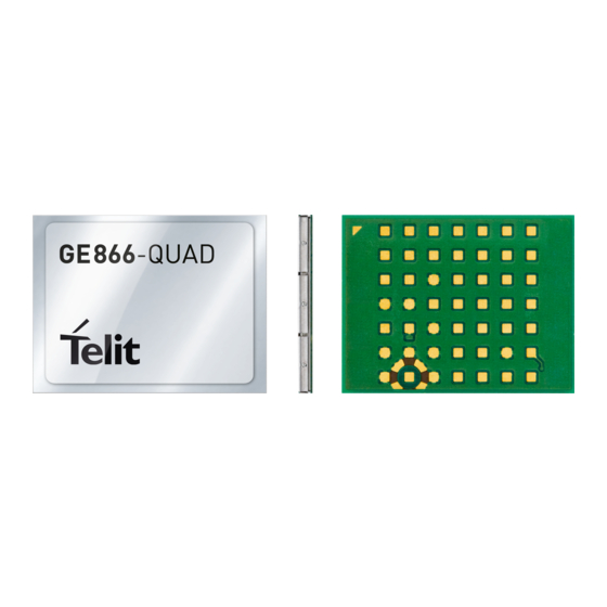
GE866-DUAL Hardware User Guide 1VV0301051 Rev. 2 – 2014-04-07 GE866-QUAD Mechanical Dimensions The GE866-QUAD overall dimensions are: • Length: 17.2 mm • Width: 13.2 mm • Thickness: 2.1 mm • Weight: 1.5 g Figure 1 Reproduction forbidden without written authorization from Telit Communications S.p.A. - All Rights Reserved. -
Page 13: Ge866-Quad Module Connections
GE866-DUAL Hardware User Guide 1VV0301051 Rev. 2 – 2014-04-07 GE866-QUAD module connections 4.1. PIN-OUT Signal Function Note Type Audio EAR- Earphone signal output, phase - Audio EAR+ Earphone signal output, phase + Audio MIC- Mic. signal input; phase- Audio MIC+ Mic. - Page 14 GE866-DUAL Hardware User Guide 1VV0301051 Rev. 2 – 2014-04-07 Signal Function Note Type 1.8V stabilized output Imax=100mA V_AUX / PWRMON Power Out 1.8V / Power ON monitor Antenna Antenna pad – 50 GPIO GPIO01 Configurable GPIO GPIO_01 / DVI_WA0 CMOS 1.8V / Digital Audio Interface (WA0) GPIO02 I/O pin GPIO_02 / JDR /...
- Page 15 GE866-DUAL Hardware User Guide 1VV0301051 Rev. 2 – 2014-04-07 WARNING: VAUX output must not be used to supply any device on the customer application. It is only provided as reference/supply voltage when voltage translation to 1V8 CMOS is needed. When its use is necessary, it is strongly recommended to connect VAUX through a series resistor as closed as possible to the module in order to reduce the inrush current of the internal DC/DC supply.
-
Page 16: Pin Layout
GE866-DUAL Hardware User Guide 1VV0301051 Rev. 2 – 2014-04-07 4.2. Pin Layout TOP VIEW C105/RTS C106/CTS TXD_AUX VABTT_PA C108/DTR C109/DCD RXD_AUX VABTT C107/DSR C125/RING RESERVED GPIO_06/ GPIO_07/ C103/TXD ALRM/ RESERVED DAC_OUT ADC_IN RESET* STAT_LED BUZZER GPIO_04/ GPIO_05/ GPIO_01/ C104/RXD TX_DIS/ RESERVED VRTC RESERVED... -
Page 17: Hardware Commands
GE866-DUAL Hardware User Guide 1VV0301051 Rev. 2 – 2014-04-07 Hardware Commands 5.1. Auto-Turning ON the GE866-QUAD Auto-turn GE866-QUAD, power supply must applied on the power pins VBATT and VBATT_PA, after 1000 m- seconds, the V_AUX / PWRMON pin will be at the high logic level and the module can be considered fully operating. - Page 18 In order to prevent a back powering effect it is recommended to avoid having any HIGH logic level signal applied to the digital pins of the GE866-QUAD when the module is powered OFF or during an ON/OFF transition. A flow chart showing the AT commands managing procedure is...
-
Page 19: Turning Off The Ge866-Quad
GE866-DUAL Hardware User Guide 1VV0301051 Rev. 2 – 2014-04-07 5.2. Turning OFF the GE866-QUAD Turning off of the device can be done in two ways: • General turn OFF • Processor turn OFF General turn OFF – disconnect the power supply from the both power pins VBATT and VBATT_PA at the same time. - Page 20 In order to prevent a back powering effect it is recommended to avoid having any HIGH logic level signal applied to the digital pins of the GE866-QUAD when the module is powered off or during an ON/OFF transition. Reproduction forbidden without written authorization from Telit Communications S.p.A. - All Rights Reserved.
-
Page 21: Resetting The Ge866-Quad
SIM responses. To unconditionally reboot the GE866-QUAD, the pad RESET* must be tied low for at least 200 milliseconds and then released. - Page 22 GE866-DUAL Hardware User Guide 1VV0301051 Rev. 2 – 2014-04-07 In the following flow chart is detailed the proper restart procedure: Modem Reset Proc. Reset = LOW Delay 200ms Reset = HIGH Delay 1s Start AT CMD. NOTE: In order to prevent a back powering effect it is recommended to avoid having any HIGH logic level signal applied to the Reproduction forbidden without written authorization from Telit Communications S.p.A.
- Page 23 GE866-DUAL Hardware User Guide 1VV0301051 Rev. 2 – 2014-04-07 digital pins of the GE866-QUAD when the module is powered OFF or during an ON/OFF transition. Reproduction forbidden without written authorization from Telit Communications S.p.A. - All Rights Reserved. Page 23 of 82...
-
Page 24: Power Supply
GE866-DUAL Hardware User Guide 1VV0301051 Rev. 2 – 2014-04-07 Power Supply power supply circuitry board layout very important part in the full product design and they strongly reflect on the product overall performance, hence read the requirements carefully and the guidelines that will follow for a proper design. - Page 25 GE866-DUAL Hardware User Guide 1VV0301051 Rev. 2 – 2014-04-07 logic level and the module can be consider fully operating. See Par. 5.1. Reproduction forbidden without written authorization from Telit Communications S.p.A. - All Rights Reserved. Page 25 of 82 Mod. 0805 2011-07 Rev.2...
-
Page 26: Power Consumption
GE866-DUAL Hardware User Guide 1VV0301051 Rev. 2 – 2014-04-07 6.2. Power Consumption The GE866-QUAD preliminary power consumptions are: GE866-QUAD Average Mode Mode description (mA) SWITCHED OFF Module power supplied only on VBATT_PA pin, the VBATT pin Typical 2uA Switched Off is not power supplied. -
Page 27: General Design Rules
(usually a tantalum one) is rated at least 10V. • A protection diode should be inserted close to the power input, in order to save the GE866-QUAD from power polarity inversion. Reproduction forbidden without written authorization from Telit Communications S.p.A. - All Rights Reserved. - Page 28 • A protection diode should be inserted close to the power input, in order to save the GE866-QUAD from power polarity Reproduction forbidden without written authorization from Telit Communications S.p.A. - All Rights Reserved. Page 28 of 82...
- Page 29 The desired nominal output for the power supply is 3.8V and the maximum voltage allowed is 4.2V, hence a single 3.7V Li-Ion cell battery type is suited for supplying the power to the Telit GE866-QUAD module. WARNING: Reproduction forbidden without written authorization from Telit Communications S.p.A. - All Rights Reserved.
-
Page 30: Thermal Design Guidelines
DON'T USE any Ni-Cd, Ni-MH, and Pb battery types directly connected with GE866-QUAD. Their use can lead to overvoltage on the GE866-QUAD and damage it. USE ONLY Li-Ion battery types. • A Bypass low ESR capacitor of adequate capacity must be provided in order to cut the current absorption peaks, a 100µF tantalum capacitor is usually suited. - Page 31 GE866-DUAL Hardware User Guide 1VV0301051 Rev. 2 – 2014-04-07 For the heat generated by the GE866-QUAD, you can consider it to be during transmission 1W max during CSD/VOICE calls and 2W max during class10 GPRS upload. This generated heat will be mostly conducted to the ground plane under the GE866-QUAD;...
-
Page 32: Power Supply Pcb Layout Guidelines
• The Bypass low ESR capacitor must be placed close to the Telit GE866-QUAD power input pads or in the case the power supply is a switching type it can be placed close to the inductor to cut the ripple provided the PCB trace from the capacitor to the GE866-QUAD is wide enough to ensure a dropless connection even during the 2A current peaks. - Page 33 GE866-DUAL Hardware User Guide 1VV0301051 Rev. 2 – 2014-04-07 • The placement of the power supply on the board should be done in such a way to guarantee that the high current return paths in the ground plane are not overlapped to any noise sensitive circuitry as the microphone amplifier/buffer or earphone amplifier.
-
Page 34: Antenna
7.1. GSM Antenna Requirements suggested Product Description antenna antenna transmission line on PCB for a Telit GE866-QUAD device shall fulfill the following requirements: ANTENNA REQUIREMENTS 824-894 MHz GSM850 band 880-960 MHz GSM900 band Frequency range 1710-1885MHz DCS1800 band 1850-1990MHz PCS1900 band... - Page 35 In the case that the antenna is not directly developed on the same PCB, hence directly connected at the antenna pad of the GE866-QUAD, then a PCB line is needed in order to connect with it or with its connector.
- Page 36 The ground around the antenna line on PCB has to be strictly connected to the Ground Plane by placing vias every 2mm at least; • Place EM noisy devices as far as possible from GE866-QUAD antenna line; • Keep the antenna line far away from the GE866-QUAD power supply lines;...
-
Page 37: Pcb Design Guidelines
7.2.1. Transmission line design During design GE866-QUAD interface board, placement of components has been chosen properly, in order to keep the line length as short as possible, thus leading to lowest power losses possible. A Grounded Coplanar Waveguide... -
Page 38: Transmission Line Measurements
GE866-QUAD RF output; a SMA connector has been soldered to the board in order to characterize the losses of the transmission line including the connector itself. During Return Loss / impedance measurements, the transmission line has been terminated to 50 Ω... -
Page 39: Gsm Antenna - Installation Guidelines
GE866-DUAL Hardware User Guide 1VV0301051 Rev. 2 – 2014-04-07 Insertion Loss of G-CPW line plus SMA connector is shown below: 7.3. GSM Antenna - installation Guidelines • Install the antenna in a place covered by the GSM signal. • Antenna shall not be installed inside metal cases •... -
Page 40: Logic Levels Specifications
1VV0301051 Rev. 2 – 2014-04-07 Logic levels specifications Where not specifically stated, all the interface circuits work at 1.8V CMOS logic levels. The following table shows the logic level specifications used GE866-QUAD interface circuits: Parameter Input level on any digital pin -0.3V +2.1V (CMOS 1.8) when on... -
Page 41: Reset Signal
It may only be used to reset a device already on that is not responding to any command. NOTE: Do not use this signal to power OFF the GE866-QUAD. Use the ON/OFF procedure to perform this function. Signal RESET* Input high 1.8V(NOTE1) 2.1V... - Page 42 GE866-DUAL Hardware User Guide 1VV0301051 Rev. 2 – 2014-04-07 Reproduction forbidden without written authorization from Telit Communications S.p.A. - All Rights Reserved. Page 42 of 82 Mod. 0805 2011-07 Rev.2...
-
Page 43: Serial Ports
The only configuration that doesn't need a level translation is the 1.8V UART. The serial port on the GE866-QUAD is a +1.8V UART with all the 8 RS232 signals. It differs from the PC-RS232 in the signal polarity (RS232 is reversed) and levels. The levels for the... - Page 44 1.5V 1.9V Input low level 0.35V Output high level V 1.6V 1.9V Output low level V 0.2V The signals of the GE866-QUAD serial port are: RS232 Pin Signal GE866-QUAD Name Usage Number Pad Number Output from the GE866-QUAD that DCD - dcd_uart...
- Page 45 In order to avoid a back powering effect it is recommended to avoid having any HIGH logic level signal applied to the digital pins of the GE866-QUAD when the module is powered off or during an ON/OFF transition. Reproduction forbidden without written authorization from Telit Communications S.p.A. - All Rights Reserved.
-
Page 46: Rs232 Levels Translation
GE866-DUAL Hardware User Guide 1VV0301051 Rev. 2 – 2014-04-07 9.2. RS232 levels translation In order to interface the GE866-QUAD with a PC com port or a RS232 (EIA/TIA-232) application level translator required. This level translator must: • invert the electrical signal in both directions;... - Page 47 GE866-DUAL Hardware User Guide 1VV0301051 Rev. 2 – 2014-04-07 An example of RS232 level adaptation circuitry could be done using a MAXIM transceiver (MAX218). In this case the chipset is capable to translate directly from 0/1.8V to the RS232 levels (Example done on 4 signals only). The RS232 serial port lines are usually connected to a DB9 connector with the following layout: Reproduction forbidden without written authorization from Telit Communications S.p.A.
-
Page 48: Audio Section Overview
GE866-DUAL Hardware User Guide 1VV0301051 Rev. 2 – 2014-04-07 Audio Section Overview 10.1. MIC Connection The Base Band Chip of the GE866-QUAD provides one input for audio to be transmitted (Uplink). 10.2. EAR Connection EAR+ OUTPUT EAR- TELIT MODULE audio... - Page 49 (it increases the W/Vrms ratio). If this were not enough, an external amplifier should be used. WARNING: This The audio output hardware of the GE866-QUAD is based on a Class-D amplifier so any singled-end output configuration MUST NOT BE USED, otherwise the presence of GSM buzzing and low level audio performance will result.
-
Page 50: Electrical Characteristics
GE866-DUAL Hardware User Guide 1VV0301051 Rev. 2 – 2014-04-07 EAR+ OUTPUT EAR- TELIT MODULE HiZ CIRCUITRY R-C filtering for HIGH impedance load. 10.3. Electrical Characteristics 10.3.1. Input lines Microphone/Line-in path Line Type Differential Coupling capacitor ≥ 100nF Differential input resistance Levels To have 0 dBfs @1KHz Differential input voltage... -
Page 51: Output Lines
GE866-DUAL Hardware User Guide 1VV0301051 Rev. 2 – 2014-04-07 10.3.2. Output lines EAR/Line-out Output Direct connection (V =1.7÷2.1V) Differential line coupling ≥ 8 output load resistance signal bandwidth 250÷3400Hz (@ -3dB with default filter) max. differential output voltage 1120 mV @3.14dBm0 (*) differential output voltage 550mV... -
Page 52: General Purpose I/O
Input pads can be read; they report the digital value (high or low) present on the pad at the read time. Output pads can only be written or queried and set the value of the pad output. An alternate function pad is internally controlled GE866-QUAD firmware acts depending function implemented. -
Page 53: Gpio Logic Levels
GPIO Logic Levels Where not specifically stated, all the interface circuits work at 1.8V CMOS logic levels. The following table shows the logic level specifications used in the GE866-QUAD interface circuits: Parameter Input level on any digital pin -0.3V +2.1V (CMOS 1.8) when on... -
Page 54: Using A Gpio Pad As Input
NOTE: In order to avoid a back powering effect it is recommended to avoid having any HIGH logic level signal applied to the digital pins of the GE866-QUAD when the module is powered OFF or during an ON/OFF transition. TIP: The V_AUX / PWRMON pin can be used for input pull up reference or/and for ON monitoring. -
Page 55: Using The Rftxmon Output Gpio5
ALARM • BUZZER The GPIO6 pad, when configured as Alarm Output, is controlled by the GE866-QUAD module and will rise when the alarm starts and fall after the issue of a dedicated AT command. This output can used to controlling microcontroller or application at the alarm time. - Page 56 GE866-DUAL Hardware User Guide 1VV0301051 Rev. 2 – 2014-04-07 The GPIO6 pad, when configured as Buzzer Output, is controlled by the GE866-QUAD module and will drive a Buzzer driver with appropriate square waves. This permits to your application to easily implement Buzzer...
-
Page 57: Magnetic Buzzer Concepts
GE866-DUAL Hardware User Guide 1VV0301051 Rev. 2 – 2014-04-07 11.7. Magnetic Buzzer Concepts 11.7.1. Short Description A magnetic Buzzer is a sound-generating device with a coil located in the magnetic circuit consisting of a permanent magnet, an iron core, a high permeable metal disk and a vibrating diaphragm. -
Page 58: Frequency Behaviour
GE866-DUAL Hardware User Guide 1VV0301051 Rev. 2 – 2014-04-07 11.7.2. Frequency Behaviour The frequency behavior represents the effectiveness of the reproduction of the applied signals. Because performance is related to a square driving waveform (whose amplitude varies from 0V to Vpp), if you modify the waveform (e.g. from square to sinus) the frequency response will change. -
Page 59: Stat Led Indication Of Network Service Availability
STAT LED Indication of network service availability STAT_LED status shows information network service availability and Call status. GE866-QUAD modules, STAT_LED usually needs external transistor to drive an external LED. Therefore, the status indicated in the following table is reversed with respect to the pin status. -
Page 60: Simin Detect Function
GE866-DUAL Hardware User Guide 1VV0301051 Rev. 2 – 2014-04-07 11.9. SIMIN detect function All the GPIO pins can be used as SIM DETECT input. The AT Command used to enable the function is: AT#SIMINCFG Use the AT command AT#SIMDET=2 to enable the SIMIN detection command AT&W0 AT&P0... -
Page 61: Dac And Adc Section
DAC and ADC section 12.1. DAC Converter 12.1.1. Description The GE866-QUAD provides a Digital to Analog Converter. The signal (named DAC_OUT) is available on pin E4 of the GE866- QUAD. The on board DAC is a 10 bit converter, able to generate an analogue value based on a specific input in the range from 0 up to 1023. -
Page 62: Low Pass Filter Example
0÷2 volts applied on the ADC pin input, store and convert it into 11 bit word. Units Input Voltage range Volt AD conversion bits Resolution > 1 GE866-QUAD module provides Analog Digital Converters. The input line is: ADC_IN Available on pin F4 Reproduction forbidden without written authorization from Telit Communications S.p.A. -
Page 63: Using Adc Converter
GE866-DUAL Hardware User Guide 1VV0301051 Rev. 2 – 2014-04-07 12.2.2. Using ADC Converter An AT command is available to use the ADC function. The command is AT#ADC=1,2 The read value is expressed in mV Refer to SW User Guide or AT Commands Reference Guide for the full description of this function. -
Page 64: Mounting The Ge866 On Your Board
GE866-DUAL Hardware User Guide 1VV0301051 Rev. 2 – 2014-04-07 Mounting the GE866 on your Board 13.1. General The GE866 modules have been designed in order to be compliant with a standard lead-free SMT process. 13.2. Module finishing & dimensions Surface finishing Ni/Au for all solder pads Dimensions in mm Reproduction forbidden without written authorization from Telit Communications S.p.A. -
Page 65: Recommended Foot Print For The Application
GE866-DUAL Hardware User Guide 1VV0301051 Rev. 2 – 2014-04-07 13.3. Recommended foot print for the application (dimensions in mm): Top View In order to easily rework the GE866 is suggested to consider on the application a 1.5 mm placement inhibit area around the module. -
Page 66: Stencil
GE866-DUAL Hardware User Guide 1VV0301051 Rev. 2 – 2014-04-07 13.4. Stencil Stencil’s apertures layout can be the same of the recommended footprint (1:1), we suggest a thickness of stencil foil ≥ 120 µm. 13.5. PCB pad design Non solder mask defined (NSMD) type is recommended for the solder pads on the PCB. -
Page 67: Recommendations For Pcb Pad Dimensions (Mm)
GE866-DUAL Hardware User Guide 1VV0301051 Rev. 2 – 2014-04-07 13.6. Recommendations for PCB pad dimensions (mm): Solder resist openings Reproduction forbidden without written authorization from Telit Communications S.p.A. - All Rights Reserved. Page 67 of 82 Mod. 0805 2011-07 Rev.2... - Page 68 GE866-DUAL Hardware User Guide 1VV0301051 Rev. 2 – 2014-04-07 It is not recommended to place via or micro-via not covered by solder resist in an area of 0,3 mm around the pads unless it carries same signal itself (see following figure).
-
Page 69: Solder Paste
GE866-DUAL Hardware User Guide 1VV0301051 Rev. 2 – 2014-04-07 tin-lead solder paste on the described surface plating is better compared to lead-free solder paste. It is not necessary to panel the application PCB, however in that case suggested milled contours predrilled board breakouts;... -
Page 70: Ge866 Solder Reflow
GE866-DUAL Hardware User Guide 1VV0301051 Rev. 2 – 2014-04-07 13.8. GE866 Solder reflow Recommended solder reflow profile Profile Feature Pb-Free Assembly Average ramp-up rate (TL to 3°C/second max Preheat – Temperature Min (Tsmin) 150°C – Temperature Max (Tsmax) 200°C – Time (min to max) (ts) 60-180 seconds Tsmax to TL –... - Page 71 GE866-DUAL Hardware User Guide 1VV0301051 Rev. 2 – 2014-04-07 Peak Temperature (tp) Ramp-down Rate 6°C/second max. Time 25°C to Peak Temperature 8 minutes max. NOTE: All temperatures refer to topside of the package, measured on the package body surface WARNING: The GE866 module withstands one reflow process only Reproduction forbidden without written authorization from Telit Communications S.p.A.
-
Page 72: Packing System
GE866-DUAL Hardware User Guide 1VV0301051 Rev. 2 – 2014-04-07 Packing system 14.1. Packing on reel The GE866 modules are packaged on reels of 500 pieces each (TBC). Reproduction forbidden without written authorization from Telit Communications S.p.A. - All Rights Reserved. Page 72 of 82 Mod. -
Page 73: Packing On Tray
GE866-DUAL Hardware User Guide 1VV0301051 Rev. 2 – 2014-04-07 14.2. Packing on tray The GE866 modules are packaged on trays of 50 pieces each when small quantities are required (i.e. for test and evaluation purposes). Trays are not designed to be used in SMT processes for pick and place handling. -
Page 74: Moisture Sensibility
GE866-DUAL Hardware User Guide 1VV0301051 Rev. 2 – 2014-04-07 14.3. Moisture sensibility The moisture sensitivity level of the Product is “3” according with standard IPC/JEDEC J-STD-020, take care of all the relative requirements for using this kind of components. Moreover, the customer has to take care of the following conditions: a) The shelf life of the Product inside of the dry bag is 12 months from seal date,... -
Page 75: Conformity Assessment Issues
GE866-DUAL Hardware User Guide 1VV0301051 Rev. 2 – 2014-04-07 Conformity Assessment Issues European Union - Directive 1999/5/EC The GE866 QUAD complies with the essential requirements of the 1999/5/EC Directive. Bulgarian С настоящето Telit Communications S.p.A. декларира, че Dual Band GSM/GPRS module отговаря... - Page 76 GE866-DUAL Hardware User Guide 1VV0301051 Rev. 2 – 2014-04-07 Lithuanian Šiuo Telit Communications S.p.A. deklaruoja, kad šis Dual Band GSM/GPRS module atitinka esminius reikalavimus ir kitas 1999/5/EB Direktyvos nuostatas. Maltese Hawnhekk, Telit Communications S.p.A., jiddikjara li dan Dual Band GSM/GPRS module jikkonforma mal-ħtiġijiet essenzjali u ma provvedimenti oħrajn relevanti li hemm fid- Dirrettiva 1999/5/EC.
-
Page 77: Ge866-Quad
The full declaration of conformity can be found on the following address: http://www.telit.com/ There is no restriction for the commercialisation of the GE866-QUAD module in all the countries of the European Union. Final product integrating this module must be assessed against essential requirements of the 1999/5/EC (R&TTE) Directive. - Page 78 GE866-DUAL Hardware User Guide 1VV0301051 Rev. 2 – 2014-04-07 Using a maximum antenna gain less or equal to than the one shown in the table below, with a minimum distance of 20 cm between the human body and antenna, the product complies with the European Council Recommendation 1999/519/EC on the limitation of exposure of the general public to electromagnetic fields (0 Hz to 300 GHz).
- Page 79 GE866-DUAL Hardware User Guide 1VV0301051 Rev. 2 – 2014-04-07 FCC/IC Regulatory notices Modification statement Telit has not approved any changes or modifications to this device by the user. Any changes or modifications could void the user’s authority to operate the equipment. Telit n’approuve aucune modification apportée à...
- Page 80 GE866-DUAL Hardware User Guide 1VV0301051 Rev. 2 – 2014-04-07 FCC Class B digital device notice This equipment has been tested and found to comply with the limits for a Class B digital device, pursuant to part 15 of the FCC Rules. These limits are designed to provide reasonable protection against harmful interference in a residential installation.
-
Page 81: Safety Recommendations
GE866-DUAL Hardware User Guide 1VV0301051 Rev. 2 – 2014-04-07 Safety Recommendations READ CAREFULLY Be sure the use of this product is allowed in the country and in the environment required. The use of this product may be dangerous and has to be avoided in the following areas: •... -
Page 82: Document History
GE866-DUAL Hardware User Guide 1VV0301051 Rev. 2 – 2014-04-07 Document History Revision Date Changes Rev. 0 2013-10-02 First issue Rev. 1 2014-02-07 Updated VRTC voltage, power consumption and packing system Rev.2 2014-03-03 Added par.15 Reproduction forbidden without written authorization from Telit Communications S.p.A. - All Rights Reserved.
Need help?
Do you have a question about the GE866-QUAD and is the answer not in the manual?
Questions and answers