Table of Contents
Advertisement
Quick Links
Introduction
PL360G55CB-EK is an evaluation kit for the PL360 modem. PL360 is a programmable modem for
narrow-band Power Line Communication (PLC) from Microchip Technology Inc, able to run any PLC
protocol in the frequency band below 500 kHz. The PL360 has been conceived to be driven by external
Microchip host controller devices; in this case a SAMG55 ARM
Microchip host device loads the corresponding PLC-protocol firmware and then controls the PL360
modem operation.
The PL360G55CB-EK board has been conceived to communicate in CENELEC B-Band (95 kHz to 125
kHz) and it complies with CENELEC standard EN 50065 regulations and Smart Energy applications. It
can be connected directly to AC mains or DC power rails.
Contents
• Welcome letter
• Board:
– One PL360G55CB-EKv2 board
• Cable:
– One Micro A/B-type USB cable
Features
• PL360G55CB-EK board mounts a PL360 PLC transceiver and a SAMG55J19 ARM Cortex M4
microcontroller.
• PL360G55CB-EK board provides a full featured platform to develop a complete communications
system based on PLC technology working in CENELEC B-Band.
• PL360 is a compact and highly efficient device for a wide range of Smart Grid applications such as
lighting control, industrial/home automation and renewable-energy management, among others.
• PL360G55CB-EK board provides support for:
– PLC band characterization and noise level measurement
– PLC sensitivity level measurement
– Power consumption
– Power fail detection
• PL360G55CB-EK board includes a SWD/JTAG interface for MCU debugging and programming
purposes. Firmware is also upgradable via USB/serial interface
• USB 2.0 full-speed interface
©
2019 Microchip Technology Inc.
PL360G55CB-EK User Guide
• Jumpers:
• Pin Headers:
User Guide
PL360G55CB-EK
®
®
Cortex
-M4 RISC processor is used. The
– Two jumpers with pitch 1.27 mm
– Two 8-pin headers with pitch 2.54 mm
DS50002871A-page 1
Advertisement
Table of Contents

Related Manuals for Microchip Technology PL360G55CB-EK


Summary of Contents for Microchip Technology PL360G55CB-EK
-
Page 1: Introduction
PL360G55CB-EK User Guide Introduction PL360G55CB-EK is an evaluation kit for the PL360 modem. PL360 is a programmable modem for narrow-band Power Line Communication (PLC) from Microchip Technology Inc, able to run any PLC protocol in the frequency band below 500 kHz. The PL360 has been conceived to be driven by external ®... - Page 2 • mikroBUS add-on connectors to integrate the board itself as a module for interfacing with other microcontrollers or microprocessors (mikroBUS main board). • PL360G55CB-EK board can be externally supplied by: – mikroBUS connector – Micro-B USB connector – DC Jack connector...
-
Page 3: Table Of Contents
Electrical Specifications........................4 2. Getting Started......................6 2.1. Powering-Up the Board........................ 6 2.2. Running Preloaded Firmware.......................7 2.3. Code and Technical Support......................7 3. PL360G55CB-EK Board....................9 3.1. Overview............................9 3.2. Features List..........................9 3.3. Hardware Description – System....................16 3.4. Hardware Description – MCU Peripherals................. 26 3.5. -
Page 4: Evaluation Kit Specifications
Evaluation Kit Specifications Safety Recommendations This evaluation board must only be used by expert technicians. The PL360G55CB-EK board is powered from a DC power source, so only the PLC coupling stage could have a hazardous voltage when is connected to mains. The risk of electric shock is minimized since all required connectors and configuration jumpers are galvanically isolated from the coupling stage. - Page 5 PL360 and SAMG55J19 devices. All PCB is supplied in the worst consumption conditions (board is supplied with a minimum input voltage, 6 V ) and emitting in CENELEC B-band. Refer to PL360 and SAMG55 datasheets for their respective power consumption. User Guide DS50002871A-page 5 © 2019 Microchip Technology Inc.
-
Page 6: Getting Started
Unpack and inspect the kit carefully. Figure 2-1. Unpacked PL360G55CB-EK Kit contents are covered by anti-static foam. The PL360G55CB-EK board is shipped in an anti-static shielding bag. The board must not be subject to high electrostatic discharge. We recommend using a... -
Page 7: Running Preloaded Firmware
• DC voltage (from +6V to +30V) from DC Jack connector (J8) Running Preloaded Firmware Once the board is supplied, LEDs will show activity. The PL360G55CB-EK board is delivered with a pre- programmed application in SAMG55 Flash memory: the G3-PLC PHY Tester for CENELEC B-Band. PLC communications are developed for CENELEC B-Band in AC or DC voltage grid. -
Page 8: User Guide Ds50002871A
Please note that the latest software code, documentation and support materials are available online. Follow instructions described in the welcome letter for more information. For any technical support requests, please visit http://support.microchip.com. User Guide DS50002871A-page 8 © 2019 Microchip Technology Inc. -
Page 9: Pl360G55Cb-Ek Board
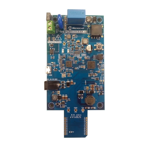
MCU, PLC coupling, peripherals and interface board. PL360G55CB-EK is a PLC modem board based on the PL360 transceiver and on the SAMG55 ARM Cortex-M4 RISC processor. This evaluation board can be used as a PLC modem reference design for modular architectures;... - Page 10 – Chip Programming jumper • Interfaces: – USB Device – mikroBUS add-on connectors – SWD/JTAG debugging port 3.2.1 PL360G55CB-EK Block Diagram The following figure shows the block diagram of the PL360G55CB-EK board. User Guide DS50002871A-page 10 © 2019 Microchip Technology Inc.
- Page 11 JTAG 10-pin Detection 3.2.2 Interface Connection The PL360G55CB-EK board includes hardware interfaces such as jumpers, connectors and a button. Following figure shows an overview of the connectors, jumpers and button of the PL360G55CB-EK board. User Guide DS50002871A-page 11 © 2019 Microchip Technology Inc.
- Page 12 PL360G55CB-EK PL360G55CB-EK Board Figure 3-3. PL360G55CB-EK Connectors, Button and Jumpers Overview PLC Connector (J1) Test Point PLC signal RESET Button (TP107) (SW1) JTAG/SWD ERASE Pin Connector (J7) Header (J3) USB Device Connector (J4) PROG Pin Header (J2) DC Input Connector (J8)
- Page 13 SPI Master Output Slave Input VCC - 3.3V power Reference Ground Table 3-4. mikroBUS Connector, J6 Mnemonic Description Hardware Interrupt UART Transmit UART Receive C Clock C Data VCC - 5V power User Guide DS50002871A-page 13 © 2019 Microchip Technology Inc.
- Page 14 This pin is normally pulled HIGH on the target to avoid unintentional resets when there is no connection. DC Input connector, J8. Table 3-6. DC Input Connector, J8 Signal Name Description DC_IN DC Input voltage (6 - 30V) Ground User Guide DS50002871A-page 14 © 2019 Microchip Technology Inc.
- Page 15 Open (closed = programming). Note: Pitch jumpers are 1.27 mm (0.050"). 3.2.2.3 Test Points Some test points (probes and pads) have been placed on the PL360G55CB-EK board for the verification of the main signals. Table 3-8. Test Point Probes Reference Function...
-
Page 16: Hardware Description - System
3.3.1 PL360 The PL360G55CB-EK board is equipped with a PL360 device in 48-pin QFN (0.4 mm pitch). PL360 is a multi-protocol (G3-PLC, PRIME 1.3 and PRIME 1.4) modem for Power Line Communication implementing a very flexible architecture, which allows implementation of standard and customized PLC solutions. - Page 17 3.3.2 SAMG55J19 The PL360G55CB-EK board is equipped with a SAMG55J19 device in 64-pin QFN. The SAM G55 devices are general-purpose low-power microcontrollers which offer high performance, processing power and small package options combined with a rich and flexible peripheral set.
- Page 18 PB08 -> Not Connected PB[0 15] Table 3-10 Table 3-11 summarize the functionality of each input/output line of the SAMG55J19 microcontroller in PL360G55CB-EK board. Table 3-10. Pinout of SAMG55J19 PortA in PL360G55CB-EK Board I/O LINE Function I/O LINE Function PL360 GPIO3...
- Page 19 Clock Circuitry Besides the embedded RC oscillators of SAMG55J19, two crystal oscillators are assembled on the PL360G55CB-EK board to obtain a more precise and stable system clock reference: • A 24 MHz clock signal, Y1, generated for the PLC transceiver PL360 •...
- Page 20 ATSAMG55J19B 3.3.4 Reset The reset sources of the PL360G55CB-EK board are: • Power-on Reset function, embedded in the SAMG55 device. • Push button reset. Both devices, SAMG55J19 and PL360, have a NRST pin: “NRST” for SAMG55J19 and “NRST_360” for PL360. The user can manually reset the SAMG55J19, which manages the PL360 reset, by using the push button SW1.
- Page 21 The PL360G55CB-EK board is assembled with the PLCOUP014-ISO coupling design. The goal is to provide a cost-optimized fully-featured design according to the G3-PLC requirements. Still, the PL360G55CB-EK board is designed to allow using all the other coupling designs by changing the corresponding components and firmware configurations.
- Page 22 The following sections describe the aim of every sub-circuit assembled in the PL360G55CB-EK board. 3.3.5.1 PLC Transmission Circuit The transmission stage adapts the EMIT signals and amplifies them. In the PL360G55CB-EK board, see Figure 3-10, it is a single branch composed of: •...
- Page 23 PLC coupling circuit connects the PLC signal directly to the mains grid or even to DC power rails without requiring any hardware adaptation. The main purpose of the circuit is to block the mains voltage of the grid to/from which the signal is injected/received. This is carried out in PL360G55CB-EK, see Figure 3-10, by a high voltage capacitor, C103.
- Page 24 PL360G55CB-EK PL360G55CB-EK Board Note that the PL360G55CB-EK board does not provide a power supply protection circuit; only a CAUTION TVS diode is used to protect from voltage spikes at the DC rail. The 12V voltage rail is obtained from the MC16301 buck-boost converter. For a further description about...
- Page 25 PLC signals by the power supply circuit. This filter also increases the input impedance, so it helps to achieve the requisites about input impedance. Notice: The PL360G55CB-EK board has PLC coupling and power supply circuits separated, so the PLC rejection filter is not included. A PLC rejection filter is needed in case of low input impedance after connecting in the same point the PLC Coupling connector J1 and the power source of the board.
-
Page 26: Hardware Description - Mcu Peripherals
PRIME1.3. Figure 3-14 shows the Zero-Crossing Detection circuit used in the PL360G55CB-EK board, which features detection of rising edges of the mains voltage. The output signal of the detection circuit “VZ CROSS” is connected to VZ pin of PL360 and a synchronization algorithm is applied in order to obtain an accurate measurement of the time between PLC frame reception and zero crossing events. - Page 27 3.4.2.2 Push Buttons The PL360G55CB-EK board is equipped with a momentary push button switch mounted directly to the board. When the button is pressed it will drive the SAMG55 reset line, NRST, to GND. And PA29 will drive the PL360 reset line, NRST_PL360, to GND.
-
Page 28: Hardware Description - Mcu Interface Ports
The USB Device Port (UDP) is compliant with the Universal Serial Bus (USB) 2.0 full-speed device specification. There is a USB available on the PL360G55CB-EK board that can act as both host and device. It has a Micro-B female USB connector with the silk screen USB. - Page 29 S as a reference for the plug-in area. The PL360G55CB-EK board is designed to operate only from the +5V power supply rail of the mikroBUS socket. Therefore, +3.3V power supply pin is not connected.
-
Page 30: Pl360G55Cb-Ek Schematics
• PL360 Schematic, Figure 3-22 • SAMG55 MCU Schematic, Figure 3-23 • Interface and Peripherals SAMG55 Schematic, Figure 3-24 • Power Supply Schematic, Figure 3-25 • PLC Coupling Schematic, Figure 3-26 User Guide DS50002871A-page 30 © 2019 Microchip Technology Inc. - Page 31 R. Navarro EMIT[0..3] EMIT[0..3] Engineer: J.L. Caceres PartNumber: Project Title PL360G55CB-EK Designed with Sheet Title PL360 Modem Size Sch #: 03-** Date: 01/04/2019 12:26:12 Revision: Sheet 2 of 6 Altium.com File: PL360.SchDoc User Guide DS50002871A-page 31 © 2019 Microchip Technology Inc.
- Page 32 PA[0..31] Engineer: J.L. Caceres PartNumber: Project Title PL360G55CB-EK Designed with Sheet Title Interface & Peripherals SAMG55 Size Sch #: 03-** Date: 01/04/2019 12:26:12 Revision: Sheet 4 of 6 Altium.com File: Interface.SchDoc User Guide DS50002871A-page 32 © 2019 Microchip Technology Inc.
- Page 33 Project Title EMIT1 PL360G55CB-EK EMIT2 EMIT3 EMIT[0..3] Designed with EMIT[0..3] Sheet Title PLC Coupling CENELEC B-Band Size Sch #: 03-** Date: 01/04/2019 12:26:13 Revision: Sheet 6 of 6 Altium.com File: PLC_Coupling.SchDoc User Guide DS50002871A-page 33 © 2019 Microchip Technology Inc.
-
Page 34: Pl360G55Cb-Ek Layout
• Layer 3: Mid Layer 2 (Power Supplies), Figure 3-29 • Layer 4: Bottom Layer, Figure 3-30 • Top Components Placement, Figure 3-31 • Bottom Components Placement, Figure 3-32 Figure 3-27. PL360G55CB-EKv2 Layout: Top Layer User Guide DS50002871A-page 34 © 2019 Microchip Technology Inc. - Page 35 PL360G55CB-EK PL360G55CB-EK Board Figure 3-28. PL360G55CB-EKv2 Layout: Mid Layer 1 (Ground) User Guide DS50002871A-page 35 © 2019 Microchip Technology Inc.
- Page 36 PL360G55CB-EK PL360G55CB-EK Board Figure 3-29. PL360G55CB-EKv2 Layout: Mid Layer 2 (Power Supplies) User Guide DS50002871A-page 36 © 2019 Microchip Technology Inc.
- Page 37 PL360G55CB-EK PL360G55CB-EK Board Figure 3-30. PL360G55CB-EKv2 Layout: Bottom Layer User Guide DS50002871A-page 37 © 2019 Microchip Technology Inc.
- Page 38 PL360G55CB-EK PL360G55CB-EK Board Figure 3-31. PL360G55CB-EKv2 Layout: Top Silkscreen User Guide DS50002871A-page 38 © 2019 Microchip Technology Inc.
- Page 39 PL360G55CB-EK PL360G55CB-EK Board Figure 3-32. PL360G55CB-EKv2 Layout: Bottom Silkscreen User Guide DS50002871A-page 39 © 2019 Microchip Technology Inc.
-
Page 40: Compliance For Specific Standards
The PL360G55CB-EK board is a CE mark product which passes the EN 50065-1, EN 50065-2-3, EN 50065-7 EMC standards. It also satisfies the Pb-Free and ROHS directive. -
Page 41: References
• MCP16301 High-Voltage Input Integrated Switch Step-Down Regulator, 2015 • MCP16301 High Voltage Buck-Boost Demo Board User’s Guide, 2012 • MCP16301 High Voltage Buck Converter 600mA Demo Board User’s Guide, 2011 User Guide DS50002871A-page 41 © 2019 Microchip Technology Inc. -
Page 42: Revision History
PL360G55CB-EK Revision History Revision History Rev A - 04/2019 Document Initial release. User Guide DS50002871A-page 42 © 2019 Microchip Technology Inc. -
Page 43: The Microchip Web Site
Microchip’s Data Sheets. Most likely, the person doing so is engaged in theft of intellectual property. • Microchip is willing to work with the customer who is concerned about the integrity of their code. User Guide DS50002871A-page 43 © 2019 Microchip Technology Inc. -
Page 44: Legal Notice
SQTP is a service mark of Microchip Technology Incorporated in the U.S.A. Silicon Storage Technology is a registered trademark of Microchip Technology Inc. in other countries. GestIC is a registered trademark of Microchip Technology Germany II GmbH & Co. KG, a subsidiary of Microchip Technology Inc., in other countries. -
Page 45: Quality Management System Certified By Dnv
PL360G55CB-EK © 2019, Microchip Technology Incorporated, Printed in the U.S.A., All Rights Reserved. ISBN: 978-1-5224-4370-4 Quality Management System Certified by DNV ISO/TS 16949 Microchip received ISO/TS-16949:2009 certification for its worldwide headquarters, design and wafer fabrication facilities in Chandler and Tempe, Arizona; Gresham, Oregon and design centers in California ®... -
Page 46: Worldwide Sales And Service
New York, NY Sweden - Stockholm Tel: 631-435-6000 Tel: 46-8-5090-4654 San Jose, CA UK - Wokingham Tel: 408-735-9110 Tel: 44-118-921-5800 Tel: 408-436-4270 Fax: 44-118-921-5820 Canada - Toronto Tel: 905-695-1980 Fax: 905-695-2078 User Guide DS50002871A-page 46 © 2019 Microchip Technology Inc.
Need help?
Do you have a question about the PL360G55CB-EK and is the answer not in the manual?
Questions and answers