Table of Contents
Advertisement
Quick Links
Introduction
PL485-EK is an evaluation kit for the PL485. PL485 is a programmable System On Chip (SOC) for narrow-band
Power Line Communication (PLC) from Microchip Technology Inc, able to run any PLC protocol in the frequency
band below 500 kHz. Depending on the running firmware, PL485 is able to support applications not only for basic
connectivity (point to point or point to multi-point connectivity) but also for complex mesh network topologies.
The PL485-EK board has been conceived to communicate in the CENELEC B-Band (95 kHz to 125 kHz) and
complies with the CENELEC EN 50065 standard. It is designed to be directly connected to low voltage DC power
rails and optionally to AC mains by means of an external coupler accessory. Please refer to
Guide
for more information about the AC coupler accessory.
Contents
•
Welcome letter
•
Board:
– One PL485-EK board
•
Cable:
– One Micro A/B-type USB cable
Kit contents are protected with anti-static foam. The PL485-EK board is shipped in an anti-static shielding bag.
The board must not be subject to high electrostatic discharges. It is recommended to use a grounding
WARNING
strap or similar ESD protective device when handling the board in hostile ESD environments. Avoid
touching the component pins or any other metallic element on the board.
Features
•
PL485-EK board includes a PL485 system on chip, able to run any PLC protocol in the <500 kHz band.
•
PL485-EK board implements a coupling circuit optimized for the band 95kHz to 125 kHz, compliant with
CENELEC standard EN50065.
•
SWD/JTAG interface for MCU debugging and programming purposes. PL485-EK board includes as well a USB
Embedded Debugger (EDBG) for on-board debugging.
•
USB 2.0 full-speed interface
™
•
mikroBUS
socket connector to interface with other circuits and add-on boards.
•
Xplained PRO header connector (master) to interface with other circuits and add-on boards.
•
RESET push button, ERASE jumper.
•
Voltage monitor circuit on the 5V rail, or alternatively on the 3.3V rail with minor modifications.
•
PL485-EK board can be powered from the following sources:
– Micro-B USB connector (J5)
– Micro-B USB connector (J12)
©
2020 Microchip Technology Inc.
PL485-EK User Guide
User Guide
PL485-EK
PLC-AC-Coupler User
DS50002954B-page 1
Advertisement
Table of Contents

Related Manuals for Microchip Technology PL485-EK


Summary of Contents for Microchip Technology PL485-EK
-
Page 1: Introduction
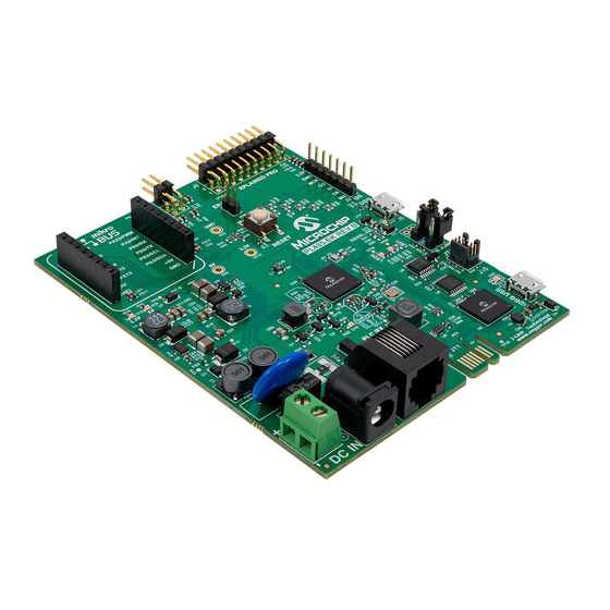
Features • PL485-EK board includes a PL485 system on chip, able to run any PLC protocol in the <500 kHz band. • PL485-EK board implements a coupling circuit optimized for the band 95kHz to 125 kHz, compliant with CENELEC standard EN50065. - Page 2 PL485-EK – Xplained PRO PWR connector (J7) – DC Jack connector (J3) or 2 position terminal block (J2) Figure 1. PL485-EK Board top view User Guide DS50002954B-page 2 © 2020 Microchip Technology Inc.
-
Page 3: Table Of Contents
Safety Recommendations......................4 1.2. Electrical Characteristics......................4 Getting Started............................5 2.1. Running the Demo Application.....................5 2.2. Code and Technical Support......................5 PL485-EK Board............................. 6 3.1. Overview............................6 3.2. Features List..........................6 3.3. Hardware Description – System....................12 3.4. Hardware Description – MCU Peripherals................. 20 3.5. -
Page 4: Evaluation Kit Specifications
This evaluation board is intended for engineering, development, demonstration or evaluation purposes only. It is not a finished product, unless otherwise noted on the board/kit, so it is intended for indoor use only. The PL485-EK board is not electrically isolated from the power supply inputs. Please handle the PL485-EK CAUTION board with care to avoid risk of electrical shock, which may arise in case of earth faults or accidental contact with high voltage on the power rail. -
Page 5: Getting Started
J2 or J3 and plug it to a DC voltage grid to communicate. Once the board is supplied, the PL485-EK board runs the pre-programmed application PLC & Go for CENELEC B- Band, a chat application between two or more end points using Microchip PLC modem boards. Any end point can transmit a message, which is received by the other end points in the network. -
Page 6: Pl485-Ek Board
PL485-EK PL485-EK Board PL485-EK Board Overview This section summarizes the PL485-EK board design. It introduces system-level concepts, such as power supply, MCU, PLC coupling, peripherals and board interfaces. Figure 3-1. PL485-EK Board Description Xplained PRO PWR connector (J7) Xplained PRO connector (J6) - Page 7 – JLINK USB Embedded MPU Programmer – Xplained PRO Master – I2S Connector 3.2.1 PL485-EK Block Diagram The following figure shows the block diagram of the PL485-EK board. Figure 3-2. PL485-EK Block Diagram Optional User LEDs (2) User Reset AC Voltage...
- Page 8 PL485-EK PL485-EK Board 3.2.2 Interface Connection The following figure shows an overview of the connectors, jumpers and button of the PL485-EK board. Figure 3-3. PL485-EK Connectors, Button and Jumpers Overview Xplained PRO PWR connector (J7) Xplained PRO connector (J6) ERASE Pin Header (J1)
- Page 9 C interface UART_RX Receiver pin of target device UART UART_TX Transmitter pin of target device UART PA16 SPI_SS_A Slave select for SPI SPI_MOSI Master out slave in line of serial peripheral interface User Guide DS50002954B-page 9 © 2020 Microchip Technology Inc.
- Page 10 C Clock UART Transmit UART Receive Hardware Interrupt PA23 Pulse-width Modulation Inter-IC Sound (I S), J9. Table 3-8. Inter-IC Sound (I S), J9 Signal Name Mnemonic Description 3.3V 3.3V VCC - 3.3V power User Guide DS50002954B-page 10 © 2020 Microchip Technology Inc.
- Page 11 Ground. Target CPU reset signal. Typically connected to the RESET pin of the target nRESET CPU, which is typically called "nRST", "nRESET" or "RESET". This signal is an active low signal. User Guide DS50002954B-page 11 © 2020 Microchip Technology Inc.
-
Page 12: Hardware Description - System
(closed = Disable JLINK enable J15 JTAG programmer) Note: Pitch jumpers are 2.54 mm (0.1"). 3.2.2.3 Test Points Some test points (probes and pads) have been placed on the PL485-EK board for the verification of the main signals. Table 3-12. Test Point Probes Reference Function... - Page 13 File: PL485.SchDoc PL_PA7/SPCK PA29 PL_PA6/NPCS0 PA30 Table 3-14 Table 3-15 summarize the functionality of each input/output line of the PL485-EK board. Table 3-14. Pinout of PL485 PortA in PL485-EK Board I/O LINE Function I/O LINE Function PA0/I2SCK0/TIOA0 I2SCK0 / PWM+ (XPLAIN)
- Page 14 PA13/MOSI5 SPI5_MOSI (mikroBUS) PA29/SPCK7 PL_SPCK PA14/SPCK5 SPI5_SPCK (mikroBUS) PA30/NPCS07 PL_NPCS0 PA15/SPCK2 SPI2_SPCK (XPLAIN) PA31 PA31(UserLed0) Table 3-15. Pinout of PL485 PortB in PL485-EK Board I/O LINE Function I/O LINE Function PB0/TXD6 UART_TX (XPLAIN) PB8/TXD4/XOUT UART_TX (mikroBUS) PB1/RXD6 UART_RX (XPLAIN) PB9/RXD4/XIN UART_RX (mikroBUS)
- Page 15 Microchip reference design for a non-isolated coupling in CENELEC-B band without external amplifier, including some modifications to couple the PLC signal to a DC BUS instead to the 220 Vac mains. PL485-EK operates with PL485 internal PLC driver, with no additional external amplification.
- Page 16 PL_AGC AGND Note: PLC coupling circuitry adds the yellow LED, D15, for visual indication of PLC frames transmission. The following sections describe the aim of each sub-circuit assembled in the PL485-EK board. 3.3.2.1 PLC Filtering Circuit The in-band flat response filtering stage reduces spurious emission to the limits set by the corresponding regulation and blocks potential interferences from other transmission channels without distorting the injected signal.
- Page 17 3.3.3 Clock Circuitry PA19 PA19 PA20 PA20 PA20 MPL485A-I/AJA DUSB_N Besides the embedded RC oscillators of the PL485, two crystal oscillators are assembled on the PL485-EK board to PA21/DM DUSB_N DUSB_P PA22/DP DUSB_P PA23 Balls connection 2/DP obtain a more precise and stable system clock reference:...
- Page 18 0.1uF PL_AGC PL_VIN PL_VIN PL_VZC PL_VZC 3.3.5 Power Supply System The PL485-EK board can be powered from several power sources, as is shown in Table 3-16. Table 3-16. Power Sources for PL485-EK Board Power Input Voltage Requirements Power Requirements Connector Marking DC Jack connector (J3) +6V to +48V (±5%)
- Page 19 PLC Coupling connector J2 and the power source of the board. The PLC rejection filter of the PL485-EK is composed of two inductors in-series (L = 560 μH) and a capacitor in- parallel (C = 0.1 μF) at the power supply input as shown in the following picture.
-
Page 20: Hardware Description - Mcu Peripherals
3V3 Buck Conver t 5V_XPLAIN 470R 3.4.2 LEDs 0.1uF User LEDs The PL485-EK board includes the following LEDs: 10uF 0.1uF • D9 and D12, connected to 5V and 3.3V supplies respectively to provide a visual status of these voltages TP19 BOOST 470R •... -
Page 21: Hardware Description - Mcu Interface Ports
The USB Device Port (UDP) is compliant with the Universal Serial Bus (USB) 2.0 full-speed device specification. 470R There is a USB available on the PL485-EK board that can act as both host and device. It has a Micro-B female USB PA[0..31] PA[0..31]... - Page 22 MOSI FB11 470R +3.3V 470R I2SMCK0 FB12 I2SDO0 I2SDI0 mikroBUS HOST I2SCK0 Drawn By: JLCF 0.1uF 0.1uF I2SWS0 Engineer: HDR-2.54 Male 1x7 JLCF User Guide DS50002954B-page 22 © 2020 Microchip Technology Inc. PartNumber: PL485-EK Sheet Title Interface Size Sch #...
-
Page 23: Hardware Description - Jlink Debugger
File: Interface&Peripheral.SchDoc The PL485-EK includes a built-in SEGGER J-Link-On-Board (J-Link-OB) device. The functionality is implemented with an ATSAM3U4C microcontroller in a TFBGA100 package. The ATSAM3U4C provides the functions of the JTAG interface and a bridge from USB to Serial debug port (known as CDC, or communication class device). The bicolored LED (D22) shows the status of the J-Link-On-Board device. - Page 24 Jumper J14 not installed: J-Link-OBD-ATSAM3U4C is enabled and fully functional. • Jumper J14 installed: J-Link-OBD-ATSAM3U4C is disabled and an external JTAG controller can be used through the 10-pin JTAG port J15. User Guide DS50002954B-page 24 © 2020 Microchip Technology Inc.
- Page 25 Size Sch #: 03-PL485 Date: 05/12/2019 15:02:00 Revision: Sheet 6 of 6 Altium.com File: JLINK debugger.SchDoc TMS/SWDIO JTAG_CONN_TMS TCK/SWCLK JTAG_CONN_TCK TDO/SWO JTAG_CONN_TDO TDI/NC JTAG_CONN_TDI GNDDetect nRESET 100R JTAG_CONN_nRST User Guide DS50002954B-page 25 © 2020 Microchip Technology Inc. C105 .1uF...
- Page 26 ENSPI 3V3_3U 3V3_3U The PL485-EK board includes an SWD (Serial Wire Debug) / JTAG interface port to provide debug level access to 150R DIS_CDC the system-on-chip. It also embeds a serial wire trace. This connector provides the required interface for in-circuit DIS_JLINK emulators, like the Atmel-ICE.
-
Page 27: Pl485-Ek Schematics
PL485-EK PL485-EK Board PL485-EK Schematics This section contains the schematics for the PL485-EK board: • Top Level Schematic, Figure 3-29 • PL485 Schematic, Figure 3-30 • Interface Schematic, Figure 3-31 • Power Supply Schematic, Figure 3-32 • PLC Coupling Schematic, Figure 3-33 •... - Page 28 PL485 - Evaluation Kit PL_AGC PL_AGC PLC_Coupling PL_VIN Sheet Title Variant Name Designed with PL_VIN PL_VZC PL485 CEN-B PL_VZC Size Sch #: 03-PL485 Date: 03/03/2020 18:10:11 Revision: Sheet 2 of 6 Altium.com File: PL485.SchDoc User Guide DS50002954B-page 28 © 2020 Microchip Technology Inc.
- Page 29 PartNumber: Project Title PL485-EK PL485 - Evaluation Kit Sheet Title Variant Name Designed with Interface CEN-B Size Sch #: 03-PL485 Date: 03/03/2020 18:10:12 Revision: Sheet 5 of 6 Altium.com File: Interface&Peripheral.SchDoc User Guide DS50002954B-page 29 © 2020 Microchip Technology Inc.
- Page 30 Project Title PL485-EK PL485 - Evaluation Kit Sheet Title Variant Name Designed with Power Supply CEN-B Size Sch #: 03-PL485 Date: 03/03/2020 18:10:12 Revision: Sheet 3 of 6 Altium.com File: Power Supply.SchDoc User Guide DS50002954B-page 30 © 2020 Microchip Technology Inc.
- Page 31 Project Title PL485-EK PL485 - Evaluation Kit Sheet Title Variant Name Designed with PLC Coupling CEN-B Size Sch #: 03-PL485 Date: 03/03/2020 18:10:12 Revision: Sheet 4 of 6 Altium.com File: PLC Coupling.SchDoc User Guide DS50002954B-page 31 © 2020 Microchip Technology Inc.
-
Page 32: Pl485-Ek Layout
03/03/2020 18:10:13 Revision: Sheet 6 of 6 Altium.com File: JLINK debugger.SchDoc PL485-EK Layout This section contains the layout graphics for the PL485-EK board: • Layer 1: Top Layer, Figure 3-35 • Layer 2: Mid Layer 1 (Ground), Figure 3-36 •... - Page 33 PL485-EK PL485-EK Board Figure 3-35. PL485-EK rev1 Layout: Top Layer Figure 3-36. PL485-EK rev1 Layout: Mid Layer 1 (Ground) User Guide DS50002954B-page 33 © 2020 Microchip Technology Inc.
- Page 34 PL485-EK PL485-EK Board Figure 3-37. PL485-EK rev1 Layout: Mid Layer 2 (Power Supplies) Figure 3-38. PL485-EK rev1 Layout: Bottom Layer User Guide DS50002954B-page 34 © 2020 Microchip Technology Inc.
- Page 35 PL485-EK PL485-EK Board Figure 3-39. PL485-EK rev1 Layout: Top Silkscreen Figure 3-40. PL485-EK rev1 Layout: Bottom Silkscreen User Guide DS50002954B-page 35 © 2020 Microchip Technology Inc.
-
Page 36: Standards Compliance
The PL485-EK board is a CE mark product which complies with EN 50065-1, EN 50065-2-3 and EN 50065-7 EMC standards. It also complies with the Pb-Free and ROHS directives. -
Page 37: References
Using PL485 to implement a fully featured G3-PLC/PRIME modem Application Note, 2020 • MCP16331 High-Voltage Input Buck Converter Evaluation Board User’s Guide, 2014 • MCP16331 Datasheet, 2016 • MCP16301/MCP16301H Data Sheet, 2015 User Guide DS50002954B-page 37 © 2020 Microchip Technology Inc. -
Page 38: Revision History
2. Getting Started Updated 2.1 Running the Demo Application section. 3. PL485-EK Board Updated Figure 3-1 3.1 Overview section. Updated Figure 3-2 3.2.1 PL485-EK Block Diagram section. Updated Figure 3-3 3.2.2 Interface Connection section. Updated Table 3-5, Table 3-6 Table 3-8 3.2.2.1 Connectors... -
Page 39: The Microchip Website
Information contained in this publication regarding device applications and the like is provided only for your convenience and may be superseded by updates. It is your responsibility to ensure that your application meets with User Guide DS50002954B-page 39 © 2020 Microchip Technology Inc. -
Page 40: Trademarks
The Adaptec logo, Frequency on Demand, Silicon Storage Technology, and Symmcom are registered trademarks of Microchip Technology Inc. in other countries. GestIC is a registered trademark of Microchip Technology Germany II GmbH & Co. KG, a subsidiary of Microchip Technology Inc., in other countries. -
Page 41: Worldwide Sales And Service
New York, NY Tel: 46-31-704-60-40 Tel: 631-435-6000 Sweden - Stockholm San Jose, CA Tel: 46-8-5090-4654 Tel: 408-735-9110 UK - Wokingham Tel: 408-436-4270 Tel: 44-118-921-5800 Canada - Toronto Fax: 44-118-921-5820 Tel: 905-695-1980 Fax: 905-695-2078 User Guide DS50002954B-page 41 © 2020 Microchip Technology Inc.
Need help?
Do you have a question about the PL485-EK and is the answer not in the manual?
Questions and answers