Tektronix 475 Instruction Manual
Hide thumbs
Also See for 475:
- Instruction manual (240 pages) ,
- Technical manual (217 pages) ,
- Instruction manual (55 pages)

Related Manuals for Tektronix 475


Summary of Contents for Tektronix 475
- Page 1 TEKTRONIX® OSCILLOSCOPE SERVICE I N S T R U C T I O N M A N U A L Tektronix, Inc. P.0. Box 500 Beaverton, Oregon Serial Number 97005 070-1332-00...
- Page 2 Tektronix, Inc. U.S.A. and Foreign T E K T R O N IX products covered by U.S. and foreign patents and/or patents pending. T E K T R O N IX is a registered trademark of Tektronix, Inc.
-
Page 3: Table Of Contents
TABLE OF CONTENTS SECTION 1 SPECIFICATIO N Page Introduction Vertical Deflection System Triggering Horizontal Deflection System 1 -2 X -Y Operation Calibrator Z Axis Input Signal Outputs Power Source Cathode-Ray Tube Environmental Supplemental Information SECTION 2 O PERATING IN F O R M A T IO N Introduction Operating Voltage Controls And Connectors... - Page 4 TABLE OF CONTENTS (cont) SECTION 3 C IR C U IT DESCRIPTION (cont) Page First 1C Amplifier Second 1C Amplifier A Trigger Generator General Trigger Source Trigger Coupling Input Source Follower Paraphase Amplifier Tunnel Diode Driver Trigger View Amplifier B Trigger Generator General Trigger Source Sweep And Z Axis Logic Circuit...
- Page 5 Sweep Timing Circuit Board Removal Recalibration After Repair Instrument Repackaging SECTION 5 C A L IB R A TIO N Calibration Interval Tektronix Field Service Using This Procedure Test Equipment Required General Special Calibration Fixtures Calibration Equipment Alternatives Preliminary Control Settings...
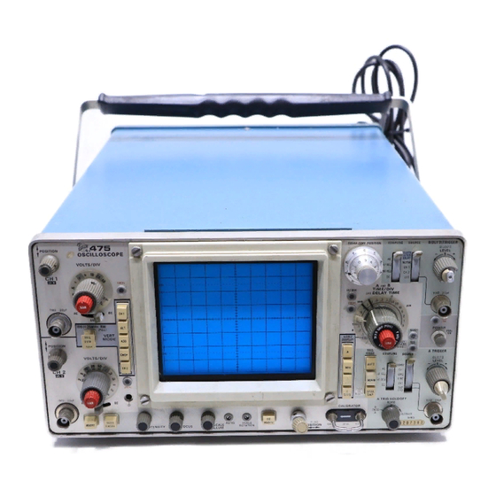
- Page 6 475 Oscilloscope...
-
Page 7: Specification
Introduction words. The horizontal deflection system has calibrated sweep rates from .5 second to .01 microsecond/division. A The 475 Oscilloscope is a wide bandwidth, portable X I 0 magnifier increases each sweep rate by a factor of 10 oscilloscope designed... -
Page 8: Horizontal Deflection System
Specification—475 LF REJ Coupled: 0.3 division internal or 100 millivolts Calibrated Sweep Accuracy (Over full ten hori zontal divisions) external from 50 kilohertz to 40 megahertz, increasing to 1.5 divisions internal or 500 millivolts external at 200 megahertz. Blocks DC and attenuates all signals below... -
Page 9: Y Operation
Specification—475 Input Resistance Delay Time And Differential Time Measurement Accuracy (Detailed) Same as vertical deflection system. Input Capacitance Same as vertical deflection system. Maximum Usable Input Voltage Same as vertical deflection system. CALIBRATO R Output approximate kilohertz repetition rate, Delay Pickoff Jitter milliampere (±2%), 300 millivolt (±1%) square-wave signal. -
Page 10: Cathode-Ray Tube
Specification—475 Humidity (Operating and Storage) line frequency of 48 to 440 hertz. Maximum power consumption is 100 watts at 115 VAC, 60 hertz. 5 cycles (120 hours) referenced to M IL-E-16400F. CATHODE-RAY TUBE Vibration Graticule Area 15 minutes along each of three major axes at a total Eight by ten centimeters. - Page 11 Specification—475 Differential Time Measurement Accuracy POSITION Control Range Exclude D E L A Y T IM E POSITION dial settings of 0.00 A t least +12 and —12 divisions from graticule center. through 0.50 for 0.5 second through 1.0 microsecond/ division delaying sweep rates.
- Page 12 Specification— 475 OUTPUT SIGNALS Geometry 0.1 division or less of tilt or bowing. Output Resistance Output resistance of the CH 2 V E R T S IG N A L OUT connector is approximately 50 ohms. Output resistance of +A and +B GATE outputs is approximately 500 ohms.
-
Page 13: Operating Information
Section 2—475 OPERATING INFORMATION Introduction To change regulating ranges, loosen the two captive screws which hold the cover onto the regulating range This section of the manual is intended to allow the selector assembly; then pull to remove the cover. -
Page 14: Controls And Connectors General
The major controls and connectors for operation of the the V O L T S /D IV switch. 475 are located on the front panel of the instrument. A few auxiliary functions are provided on the rear panel. Fig. 2-2 UNCAL Light indicates that the VAR con... - Page 15 Operating Inform ation—475 Channel 1 B Triggering m sm * ouay VO LTS/D IV Power V ertical : POSITION VO LTS /D IV 16VEL CH 2 r;SCAL£ JFOCUS : ILIUM Channel 2 A & B Calibrator A Triggering Sweep A. Front panel.
-
Page 16: A And B Triggering
Operating Information—475 DC: All components of the input HF REJ: Accepts signals between signal are passed to the Vertical 60 Hz and 50 kHz. Rejects DC Amplifier. and attenuates all signals outside the above range. Dual-purpose switch that limits the... -
Page 17: A And B Sweep
Operating Information—475 A T R IG MODE Determines the operating mode for A AND B T IM E /D IV A T IM E /D IV switch (clear plastic the A Trigger Circuit. A ND D E L A Y T IM E... -
Page 18: Calibrator And Power
The following instructions will allow the operator who is by the B T IM E /D IV switch with unfamiliar with the operation of the 475 to obtain the basic the delay time determined by displays commonly used. Before proceeding with these... -
Page 19: Magnified Sweep Display
Operating Information—475 Advance the IN T E N S IT Y control until the display is Set the H O R IZ DISPLAY switch to B D LY D . The visible. If the display is not visible with the IN T E N S IT Y... -
Page 21: Circuit Description
This section of the manual contains a description of the functions within this instrument. The function and opera circuitry used in the 475 Oscilloscope. The description tion of the logic circuits are described using logic sym begins with a discussion of the instrument, using the basic bology and terminology. -
Page 22: Block Diagram
A basic block There are three sweep generator circuits in the 475. For diagram of the 475 Oscilloscope is shown in Fig. 3-1. Only purposes of explanation, they are called Delaying, Slow the basic interconnections between the individual blocks Non-Delaying, and Fast Non-Delaying. -
Page 23: Channel 1 Preamp
Input Attenuator The effective overall deflection factor of each channel of the 475 is determined by the appropriate V O L T S /D IV CHANNEL 1 PREAMP switch setting. The basic deflection factor of the Vertical Deflection System is 5 millivolts/division of CRT deflec... -
Page 24: First Cascode Amplifier
Circuit Description—475 cies within the bandwidth of the instrument, the Input calibrated detent. The component values selected for the Attenuators are designed to maintain the same input RC variable function provide a variable attenuation ratio of characteristics for each setting of the V O L T S /D IV switch. -
Page 25: Channel 2 Preamp
Circuit Description—475 the biasing on the output transistors of U220 so that the offset compensation changes associated with variations in normally inactive transistors are now carrying the signal. ambient temperature. As temperature increases, the value Since their outputs are cross-coupled from side to side the of RT170 decreases. -
Page 26: Switching Logic Flip-Flops
Circuit Description—475 (Channel 1) of U370. The logic levels connected to pins 1, Switching Logic Flip-Flops 12, 13, and 16 determine what signals are presented at U 350A and U350B are edge-triggered flip-flops that output pins 14 and 15. The following logic truth table derive the switching logic for the Channel Switch 1C U370. -
Page 27: Chop Blanking Amplifier
Circuit Description—475 Chop Blanking Amplifier V E R TIC A L OUTPUT A M PLIFIER The Chop Blanking Am plifier Q348 provides an output General pulse to the Z Axis Amplifier circuit, which blanks out the The Vertical Output Amplifier provides the final amplifi... -
Page 28: Trigger Source
Circuit Description—475 the external trigger input connector, or a sample of the line attenuated, while the lower frequency components (be voltage connected to the instrument. Controls are provided tween about 60 Hz 50 kHz) are passed without to select trigger level, slope, coupling, and source. Fig. 3-5 attenuation. -
Page 29: Tunnel Diode Driver
Circuit Description—475 in phase with respect to the input signal. When the SLOPE Normally, the output of the Vertical Channel Switching switch is set to the — position, the output signal at pin 8 is circuit is applied to the input of the Delay Line. When the... -
Page 30: Main Gate Comparator
Circuit Description—475 Pin 2. This is the negative Auto Sense Input. A fixed DC Pin 17. This is the holdoff output terminal. The gate level established by R602 and R603 is connected here. level at this terminal is HI during holdoff and LO otherwise. -
Page 31: Z Axis Logic Multivibrator
Circuit Description—475 Delayed Latch circuit. The positive-going signal turns Q594 Sweep Generator ends its sweep and resets the Delay on which in turn turns on Q596. The positive-going signal Pickoff Comparator. In the B ENDS A position of the A at the collector of Q596 is connected to pin 16 of U 600 to T R IG H O LD O FF control +5 volts is connected to R798. -
Page 32: Sweep Generators
Circuit Description—475 Main Gate Amplifier SWEEP GENERATORS Q902 is the Main Gate Amplifier stage. The negative General going Main Gate waveform from the Sweep Logic circuit is applied to the base of Q902. The amplified and inverted The Sweep Generators produce the sawtooth voltages... -
Page 33: Sawtooth Sweep Generator
Circuit Description—475 Sawtooth Sweep Generator Logic Comparator Q920 and Q922 form a Miller Integrator circuit. When Q944 and Q946 are connected as a voltage comparator the current through the Sweep Disconnect Amplifier Q904 and generate the logic pulses that signal the end of sweep is interrupted, the timing capacitance begins to charge and blank the CRT display at the end of the sweep. -
Page 34: Non-Delaying Sweep Generators
Circuit Description—475 goes down. When it goes more negative than the level at the Q988 Q1018 are Sweep Start Amplifiers and gate of Q926A (established by the D E L A Y -TIM E POSI establish the DC level starting points for the sweeps. The TIO N control), Q926A conducts and Q926B turns off. -
Page 35: Horizontal Amplifier
Circuit Description—475 and Q 1 134 so that a center screen display does not change H O R IZO N TA L A M P LIFIE R position when the X 1 0 Magnifier is turned on. General Q1114 is a current-source that is an interruptable path The Horizontal Am plifier circuit provides the output for the horizontal positioning currents. -
Page 36: Output Amplifier
Circuit Description—475 Output Amplifier 115-volt nominal operation, or in series for 230-volt nominal operation. Line Fuse F1401 should be changed for The push-pull signal from the Gain Setting Amplifier is each nominal line voltage (current rating of fuse for connected to the Output Amplifier. Each half of the... - Page 37 Circuit Description—475 + 1 1 0 S E R IE S Fig. 3-8. Detailed block diagram of the Power Supply. 3-17...
-
Page 38: High-Voltage Regulator
Circuit Description—475 Q1318 o ff by way of the feedback voltage to the base. The If the output voltage at the —2450 volt test point starts voltage waveform at the collector of Q1318 is a sine wave to go positive (less negative), this positive-going change is at the resonant frequency of T 1320. -
Page 39: High-Voltage Rectifiers And Output
Circuit Description—475 the CRT beam after vertical deflection but before hori applied to Q1318 and prevents the amplitude of oscillations zontal deflection. Therefore, it affects only the vertical (Y) from increasing. This prevents the C RT cathode supply components of the display. TRACE R OTATIO N adjust... -
Page 40: Dc Restorer Circuit
General General The Calibrator circuit produces a square-wave output The fan motor used in the 475 is a brushless DC fan signal with accurate voltage and current amplitudes. This motor using Hall Effect devices. The fan motor circuitry output is available as a voltage or current at the C A L I... -
Page 41: Maintenance
MAINTENANCE and will improve the reliability of this instrument. The Cabinet Removal severity of the environment to which the 475 is subjected W A R N I N G will determine the frequency of maintenance. A convenient time to perform preventive maintenance is just prior to recalibration of the instrument. -
Page 42: Lubrication
Transistor Checks Exterior. Loose dust accumulated on the outside of the 475 can be removed with a soft cloth or small paint brush. Periodic checks of the transistors and other semi The paint brush is particularly useful for dislodging dirt on conductors in the 475 are not recommended. -
Page 43: Soldering Techniques
Ordinary 60/40 solder and a 35- to 40-watt pencil-type soldering iron can be used to accomplish the majority of the soldering to be done in the 475. If a higher wattage Unplug the six coaxial cables and one wire from the rating soldering iron is used on the etched circuit boards, front side of the Vertical Preamp circuit board. -
Page 44: Vertical Mode Switch Circuit Board Removal
Maintenance—475 Remove the shafts from the vertical POSITION Remove the two securing screws from the rear of the potentiometers on the Vertical Preamp circuit board. Vertical Mode Switch circuit board. Loosen the front setscrew in the couplers and pull the shafts out through the front panel. -
Page 45: Sweep Timing Circuit Board Removal
Regulating Range Selector Assembly and the two feet Instrument Repackaging from that side of the instrument. If the 475 is to be shipped for long distances by commercial means of transportation, it is recommended Unsolder the transformer leads from the Interface that the instrument be repackaged in the original manner Board and from the Regulating Range Selector Assembly. -
Page 47: Calibration
IN TER A C TIO N — part of the step. To assure instrument accuracy, check the calibration of the 475 every 1000 hours of operation, or every six months TEST EQUIPMENT REQUIRED if used infrequently. Before complete calibration, thor... - Page 48 1%. 7. Medium-Frequency Con Frequency, 350 kilohertz to Vertical system bandwidth a. Tektronix Type 191 Con stant-Amplitude Signal Gen 50 megahertz; reference fre and trigger circuits operation s ta n t - A m p lit u d e Signal erator checks.
- Page 49 P a r t N u m b e r nectors to fit input jacks of 067-0676-00. the 475 delay line. Connectors, GR874 thru- Trigger system checks and ad Tektronix Part Number 13.
-
Page 50: Preliminary Control Settings
24. Input Normalizer1 RC time constant, 20 pico Standardize input RC time Tektronix Part Number farads times 1 megohm. constant. 067-0538-00. a. Tektronix calibration fix- Dual-Input Coupler Connectors, BNC; matched Used fo r signal in te r signal transfer to each input. -
Page 51: Performance Check
Page 5-7 wise Accuracy 9. Check Channel 1 and 2 Variable Volts/ Page 5-8 Connect the 475 to a power source that meets the Division Range voltage and frequency requirements of this instrument. 10. Check Alternate Mode Operation Page 5-8 Set the controls as given under Preliminary Control 11. -
Page 52: Vertical System Check
Calibration—475 V E R TIC A L SYSTEM CHECK Equipment Required 4. GR to BNC Female Adapter. 1. Standard Amplitude Calibrator (067-0502-01). 5. 42-inch 50 £2 BNC cable (two). 2. High-Frequency Constant-Amplitude Signal Generator (067-0532-01). 6. X I 0 BNC Attenuator. -
Page 53: And 2 Position Range
Calibration—475 Check Channel 2 Inverted Balance CHECK—CRT display for 4 divisions of deflection, within 0.12 division. Set the V E R T MODE switch to CH 2 and the CH 2 AC-GND-DC switch to GND. Check Add Mode Operation Set both AC-GND-DC switches to DC. -
Page 54: Check Alternate Mode Operation
Calibration—475 c. Adjust the A LEVEL control for a stable display. CHECK-Using the CH 2 V O L T S /D IV switch and the Standard Amplitude Calibrator settings given in Table 5-2, check that the vertical deflection factor is within the given tolerance in each position of the CH 2 V O L T S /D IV switch. -
Page 55: Trigger System Check
Calibration—475 g. Repeat the bandwidth check procedure, step 12-c CH 2 input via a GR-to-BNC adapter, 42-inch 50 £2 BNC through 12-e. cable, X I 0 BNC attenuator, and a 50 £2 BNC termination. h. Disconnect the test.se.tuiL d. Adjust the Medium-Frequency signal generator for a five-division display of a 50 kilohertz signal. -
Page 56: Check B Triggering
Calibration—475 h. Set the V E R T MODE switch to CH 2 and the A d. CHECK—A stable display can be obtained on both SOURCE switch to CH 2. slopes of the displayed waveform in all positions of the B COUPLING switch by adjusting the LEVEL controls. -
Page 57: Horizontal System Check
Calibration—475 f. Remove the test signal from the CH 1 input. j. CHECK— That a single-sweep display (one sweep only) is presented. g. CHECK—For no display in the absence of an k. Disconnect the test setup. adequate trigger signal. 17. Check Single Sweep Operation 18. -
Page 58: Check Timing Accuracy
Calibration—475 CHECK—That the U NCAL light comes on when the CHECK—Using the T IM E /D IV switch, the B V A R T IM E /D IV control is out of the detent position. T IM E /D IV switch and the Time-Mark Generator settings given in Table 5-4, check that delayed sweep accuracy is within the given tolerance. -
Page 59: Check Delay Time Jitter
Calibration—475 22. Check Delay Time Jitter b. Apply a 20 m V square wave from the Standard Amplitude Calibrator to the CH 1 or X input through a a. Set the D E L A Y T IM E POSITION dial to 1.00, the 42-inch 50 £2 BNC cable. -
Page 60: Short-Form Calibration
3. Adjust CRT Grid Bias a. T R IG MODE to NORM. 2. Connect the 475 to the autotransformer and set the line voltage to 115 VAC. b. Connect DC Voltmeter to TP1364 and adjust IN T E N ... -
Page 61: Vertical System Calibration
Calibration—475 e. A DJU ST—Geometry, R1390, for no more than 0.1 b. A DJU ST—Delay-Line Driver Centering, R385 for division curvature of the time markers. reading of 0 volts on both sides of the delay line. f. Remove the time markers and check the trace at top 10. - Page 62 Calibration—475 b. Connect a 50 m V signal from the Standard Amplitude A D JU ST—CH 2 2 m V Gain, R225, for 5 divisions Calibrator to the CH 1 input. deflection, within 3%. Check all attenuator ranges for proper deflection, c.
- Page 63 Calibration—475 Connect preamp end of delay line to Signal Insertion Connect output of Fast-Rise High-Amplitude Pulse Unit (067-0676-00). Generator (Type 109) to the CH 1 input. Connect +15 V and —8 V to Signal Insertion Unit. Adjust for 5 divisions of deflection.
-
Page 64: Trigger System Calibration
Calibration—475 29. Check Bandwidth Limit Operation A DJU ST—A Trigger Center, R754, for triggering point at graticule center. Connect a 6 division display of a 50 kHz signal to the CH 1 input. Check frequency is 20 MHz, within 5 MHz, when 32. -
Page 65: Horizontal System Calibration
C alibration-475 34. Check Triggering H O R IZO N TA L SYSTEM C A LIBR ATIO N a. High-frequency triggering: Adjust Delay Start and Delay Stop Internal 40 MH 200 MHz a. A T IM E /D IV to 1 ms, 0.3 div... - Page 66 C alibration-475 A DJUST—Horizontal Gain, R1155, 1 time d. H O R IZ D ISPLA Y to A IN T E N , marker/division, within 1%, from +20°C to +30°C; for 1 time marker/division, within 3%, from —15°C to +55° C.
- Page 67 + 3 0 °C, from 0.0bps to 0.5 s, tion, around the crossed horizontal deflection leads on the accuracy is within 2%. 475. Connect the P6022 to the test oscilloscope. b. From —15°C to + 5 5°C, from 0 .0 5 to 0.5 s, d.
-
Page 68: Calibration
Calibration— 475 55. Check X -Y Phasing and Bandwidth 0.01 From —15°C to + 5 5 °C# from to 50 ms, accuracy is within 4%. a. Connect an 8 division display of 50 kHz signal from Medium-Frequency Constant-Amplitude Signal Generator to the CH 1 and 2 inputs. -
Page 69: Introduction
Calibration—475 PART I I I — C A LIBR ATIO N Introduction Page 5-31 18. Adjust Channel 1 Position Centering The following procedure returns the 475 to correct Page 5-31 19. Adjust Channel 2 Variable Volts/ calibration. All limits and tolerances given in this procedure... -
Page 70: Preliminary Procedure
62. Adjust Delay Start and Delay Stop Page 5-50 63. Check Differential Time Accuracy 1. Remove the dust cover from the 475 as outlined in the Disassembly Instructions in the Maintenance section of Page 5-50 64. Adjust Horizontal Amplifier Gain the manual. -
Page 71: Power Supply Calibration
20 minutes warmup before proceeding. N O T E 3. Connect the 475 to the autotransformer output. Titles for external controls o f this instrument are capitalized in this procedure (e.g., IN T E N S IT Y ). -
Page 72: Display & Z-Axis Calibration
Calibration—475 CHECK—For LOW LIN E indicator light to turn on when the autotransformer is below 103 volts. g. Return the autotransformer for a 115 VAC output. Check High Voltage Power Supply Connect the DC Voltmeter between the -2 4 5 0 -vo lt test point and ground (positive meter lead to ground). -
Page 73: Check Astig Control
Calibration—475 Check ASTIG Control Set the CH 1 AC-GND-DC switch to DC and the CH 1 V O L T S /D IV switch to 0.1 V. Rotate ASTIG control (front panel screwdriver adjust ment) through its range. c. Adjust the A LEV E L control for a stable display, the ASTIG and FOCUS controls for a well-defined display. -
Page 74: Vertical System Calibration
Calibration—475 IN T E R A C T IO N —Between Geometry Axis Adjust the Test Oscilloscope trigger controls to view Alignment adjustments. Adjust both for optimum response. the positive step of a 1 vplt display of the Z-Axis signal. -
Page 75: Adjust Vertical Shield Voltage
Calibration—475 g. Remove the Precision DC Voltmeter connections. 12. Adjust Delay-Line Driver Centering a. Using the Precision DC Voltmeter, monitor both ends of the delay line until the readings are equal, while adjusting the CH 1 POSITION control. b. CHECK—Precision DC Voltmeter for a reading of 0 volts. -
Page 76: Check Probe Indicator Lights
Calibration—475 c. CHECK— That the CH 1 UNC AL light turns on when d. Set the V E R T MODE switch to CH 2. the V A R control is out of the detent position. e. Move the X I 0 probe to the CH 2 input. -
Page 77: Check Channel 2 In V E R T Balance
Calibration—475 Repeat step 17-h. Return the CH 2 V A R control to the detent position. Adjust CH 1 Position Centering Adjust CH 2 Gain Switch Balance a. Set the CH 1 V O L T S /D IV switch to 2 m V. - Page 78 Calibration—475 f. CHECK— The Test Oscilloscope for a 200 m V (peak- 22. Adjust CH 2 Position Centering to-peak) signal. a. Set the CH 2 V O L T S /D IV switch to 2 mV. g. A DJU ST—CH 1 5 mV Gain adjustment, R165 (see b.
- Page 79 Calibration—475 24. Adjust CH 2 Gain TABLE 5-6 Vertical Deflection Accuracy a. Set the V E R T MODE switch to CH 2, the CH 2 V O L T S /D IV switch to 5 m V, and the AC-GND-DC switch...
-
Page 80: Check Add Mode Operation
Calibration—475 g. Rotate the CH 1 VA R control fully counterclockwise. Check A LT Mode Operation a. Set the V E R T MODE switch to A LT and the A LEV E L control fully clockwise. h. CHECK—CRT display reduces to less than 2 divisions. - Page 81 Signal Insertion Unit (067-0676-00). 31. Adjust High-Frequency Compensation Connect the Signal Insertion Unit to +15 volts and —8 volts from the 475. a. Connect the fast-rise output of the Square-Wave Generator (Type 106) to the CH 1 input via a 42-inch 50 12 BNC cable and a 50 12 BNC termination.
- Page 82 Calibration—475 Adjust the Square-Wave Generator for 5 divisions of a CAL A ID —C175 and R175 affect aberrations 10 ns 100 kHz signal. from the leading edge; C l33 and R133 affect aberrations 2 ns from the leading edge; Cl 12 and R 112 affect the front corner aberrations.
- Page 83 C alibration-475 IN T E R A C T IO N —Between Channel 2's C32 and C33. h. Turn the CH 2 V O L T S /D IV switch to 10 mV. Re-adjust both for optimum response. i. CHECK—Repeat step 32-d.
-
Page 84: Check Vertical Amplifier Bandwidth
Calibration—475 h. CHECK—Repeat step 33-d. y. C HECK—Repeat step 33-d. i. ADJUST—Channel 1's C36 and C37 (see Fig. 5-19) z. A DJU ST—Channel 1's C30 and C31 (see Fig. 5-19) with a low-capacitance screwdriver, for best corner and with a low-capacitance screwdriver, for best corner and flat-top waveform. -
Page 85: Check Vertical Channel Isolation
Calibration—475 b. Connect the CH 2 V E R T S IG N A L O U T (on the rear CHECK—CRT display for no more than 0.2 division panel) to the CH 1 input via a 42-inch 50 £2 BNC cable and of deflection. -
Page 86: Trigger System Calibration
Calibration—475 TRIG G ER SYSTEM CA LIB R A TIO N Equipment Required 8. GR-to-BNC Female Adapter. 1. Standard Amplitude Calibrator (067-0502-01). 9. 42-inch 50 £2 BNC Cable. 2. High-Frequency Constant-Amplitude Signal Generator (067-0532-01). 10. 18-inch 50 £2 BNC Cable (two). -
Page 87: Adjust B Trigger Centering And
Calibration—475 d. A DJU ST—A Trigger Centering adjustment, R534 (see c. CHECK— That a stable display can just be obtained by Fig. 5-20), for the trigger point of the display to be at the rotating the B LEVEL control. graticule center. -
Page 88: Check B Trigger Dc Balance
Calibration—475 i. Set the V E R T MODE switch to CH 2. DC positions of the B COUPLING switch by adjusting the B LEV E L control. j. Adjust the CH 2 V O L T S /D IV switch to obtain a 0.3 division display. -
Page 89: Check A External 40 Megahertz
Calibration—475 h. Set the A SOURCE switch to CH 1. I. Replace the X I 0 BNC attenuator to the test setup. i. CHECK— A stable display can be obtained on both slopes of the displayed waveform in the AC, LF REJ, and 47. -
Page 90: Check B Internal 200 Megahertz
Calibration— 475 f. Adjust the High-Frequency signal generator for a 200 c. CHECK— That a stable display, with no more than 0.2 megahertz output frequency. division of jitter, can be obtained on both slopes of the displayed waveform, by adjusting both LEVEL controls, in the AC, LF REJ, and DC positions of the B COUPLING g. -
Page 91: Check Hf Rej Triggering
Calibration—475 g. Set the V E R T MODE switch to CH 1. i. Set the A SOURCE switch to EXT. h. CHECK—Repeat step 50-b. j. CHECK— That a stable display cannot be obtained in the HF REJ position of the A COUPLING switch. -
Page 92: Check B 60 Hertz And Lf Rej
Calibration—475 52. Check B 60 Hertz and LF REJ Triggering p. C HECK—Repeat step 52-f. a. Set the B T IM E /D IV switch to 5m s, the H O R IZ DISPLAY switch to B D L Y 'D , both SOURCE switches to q. -
Page 93: Check A Lev E L Control External
Calibration—475 k. CHECK— That the display can be triggered at any n. CHECK—Repeat step 53-d. point along the negative slope of the displayed waveform, in the AC, HF REJ, and DC positions of the A COUPLING switch, when rotating the A LEVEL control throughout its o. -
Page 94: Check Normal Mode Operation
Calibration—475 b. Adjust Low-Frequency Sine-Wave Generator the A COUPLING switch to AC, and the A SLOPE switch (General Radio 1310-A) for a 50 kilohertz signal output. to +. c. Adjust the A LE V E L control for a triggered display. -
Page 95: Horizontal System Calibration
Calibration—475 Check Trigger View Deflection Factor a. Connect the output of the Standard Amplitude Calibrator to the A External Trigger input via a 42-inch 50 £2 BNC cable. b. Adjust the Standard Amplitude Calibrator for a 200 m V output. -
Page 96: Check Differential Time Accuracy
Calibration—475 f. C H E C K -D E L A Y T IM E POSITION dial for a reading e. CHECK—Intensified portion of the sweep begins at the tenth time marker. of one division less, within 0.01 division from +15°C to +35°C (one division less, within 0.02 division from —15°C... -
Page 97: Adjust Magnifier Registration
Calibration—475 CHECK—X10 MAG light is on when the X 10 MAG b. Turn the horizontal POSITION control fully clock button is in. wise. c. CHECK—Start of sweep is to the right of the center CHECK—CRT display for 1 time marker/division, vertical graticule line. -
Page 98: Adjust 0.1 Microsecond Timing
Calibration—475 CHECK— CRT display for 1 time marker/division, w ithin 2% from +20°C to +30°C; 1 time marker/division, w ithin 3% from —15°C to +55°C. ADJUST— C l025 (see Fig. 5-25) w ith low- capacitance screwdriver, for 1 time marker/division. -
Page 99: Adjust High-Speed Timing-Visual
Connect a X I 0 probe from the Test Oscilloscope to Set the A T IM E /D IV switch to 0.05 jus, the X I 0 MAG the +50 V test point on the 475 (see Fig. 5-26). button in, the A SOURCE switch to EXT, and the A COUPLING switch to LF REJ. -
Page 100: Adjust High-Speed Timing-Current
1 cycle/division. Hook the current probe around the crossed horizontal deflection leads on the 475 (see Fig. 5-29). k. Set the A TIME/D1V switch to 0.01 jus. e. Horizontally center the trace with the horizontal CHECK— CRT display for 1 cyeie/2 divisions, w ithin POSITION control. -
Page 101: Check T Im E /D Iv Accuracy
40 mA in amplitude. 73. Check T IM E /D IV Accuracy p. Set the 475 A T IM E /D IV switch to 0.01 jus. C HECK—Using the A T IM E /D IV switch and the Time-Mark Generator settings given in Table 5-7, check that q. -
Page 102: Check A Inten Timing Accuracy
Calibration—475 74. Check A INTEN Timing Accuracy CHECK—Using the T IM E /D IV switch, the B T IM E /D IV switch and the Time-Mark Generator settings a. Set the H O R IZ DISPLAY switch to A IN TEN . -
Page 103: Check Delay Time Jitter
Calibration—475 TABLE 5-10 A and B Magnified Timing Accuracy Portions of total A T IM E /D IV Time-Mark CRT Display magnified sweep Accuracy (Markers/ length to exclude Switch Generator Setting Output Division) from measurement +20° C to +30° C —15°C to +55°... -
Page 104: Adjust X -Y Phasing And Bandwidth
Calibration—475 b. Apply a 20 mV square wave from the Standard Increase the output frequency of the Medium- Am plitude Calibrator to the CH 1 or X input through a Frequency signal generator to 2 megahertz. 42-inch 50 £2 8NC cable. -
Page 105: C A L Ib R A T O R , + Gates, And E X T Z-A Xis Calib Ra
Calibration—475 c. Set the Test Oscilloscope T IM E /D IV switch so that e. CHECK—For at least nine times increase in the the bottom portion of the waveform (holdoff time of the holdoff time of the +A GATE. +A GATE) is slightly less than one division. - Page 106 Calibration—475 b. Set the IN T E N S IT Y control for a normal viewing Adjust the Medium-Frequency signal generator for a 5 level. volt (peak-to-peak) 50 kilohertz signal. CHECK—CRT display for noticeable intensity modu Connect the Medium-Frequency Constant-Amplitude lation of the positive peaks.
- Page 107 Section 6—475 ELECTRICAL PARTS LIST Replacement parts should be ordered from the Tektronix Field Office or Representative in your area. Changes to Tektronix products give you the benefit of improved circuits and components. Please include the instrument type number and serial number with each order for parts or service.
- Page 108 Electrical Parts List—475 Serial/Model No. Tektronix Ckt. No. Part No. Disc Description C A P A C I T O R S (cont) C 4 1 2 8 3 - 0 1 5 6 - 0 0 1 0 0 0 pF,...
- Page 109 Electrical Parts L is t-4 7 5 Tektronix S e ria l/M o d e l N o. Description Ckt. N o. Part N o . Disc C A P A C I T O R S (cont) C 2 3 3...
- Page 110 Electrical Parts List—475 Tektronix Serial/Model No. Ckt. No. Part No. Disc Description (cont) C 4 4 5 x 2 8 1 - 0 1 2 2 - 0 0 C 4 5 0 2 . 5 - 9 p F,...
- Page 111 Electrical Parts L is t-4 7 5 Tektronix Serial/Model No. Part No. Disc Description Ckt. N o. C A P A C I T O R S (cont) C 5 7 2 281- 0 5 0 9 - 0 0...
- Page 112 Electrical Parts List—475 Serial/Model No. Tektronix Disc Description Ckt. N o. Part N o. C A P A C I T O R S (cont) C 7 4 4 283- 0 0 0 3 - 0 0 0 . 0 1 u F , Cer ,...
- Page 113 Electrical Parts List—475 Tektronix Serial/Model Ckt. No. Part No. Disc Description C A P A C I T O R S (cont) C 1 0 2 5 2 8 1 - 0 0 9 6 - 0 0 5 . 5 - 1 8 pF,...
- Page 114 Electrical Parts List—475 Tektronix Seriaf/Model No. Ckt. No. Part No. Description Disc C A P A C I T O R S (cont) C 1 2 6 3 2 9 0 - 0 5 2 4 - 0 0 4 . 7 uF, E l e c t .
- Page 115 Electrical Parts List—475 Tektronix S e ria l/M o d e l N o. Ckt. N o. Description Part N o . Disc C A P A C I T O R S ( c o n t ) C 1 4 5 8...
- Page 116 Electrical Parts List—475 Tektronix S e ria l/M o d e l N o. Ckt. N o. Part N o. Disc Description D I O D E S (cont) C R 6 0 5 1 5 2 - 0 1 4 1 - 0 2...
- Page 117 Electrical Parts List—475 Tektronix Serial/Model No. Ckt. No. Description Pari No. Disc D I O D E S (cont) C R 9 5 2 1 5 2 - 0 1 4 1 - 0 2 S i l i c o n ,...
- Page 118 Electrical Parts L is t-4 7 5 Tektronix Serial/Model No. Ckt. No. Part No. Disc Description D I O D E S (cont) C R 1 1 8 3 1 5 2 - 0 3 2 2 - 0 0...
- Page 119 Electrical Parts List—475 Tektronix Serial/Model Ckt. No. Part No. Disc Description D I O D E S (cont) C R 1 4 7 8 1 5 2 - 0 0 6 6 - 0 0 S i l i c o n ,...
- Page 120 Electrical Parts List—475 Tektronix Serial/Model No. Ckt. No._________ Part No. Eff__________Disc_____________________ Description CONNECTORS (cont) J 6 6 4 1 3 1 - 1 0 0 3 - 0 0 R e c e p t a c l e ,...
- Page 121 Electrical Parts L is t-4 7 5 Tektronix Serial/Model No. Ckt. No. Disc Description Part No. I N D U C T O R S (cont) L 2 7 4 B 0 2 9 9 9 9 C o r e ,...
- Page 122 Electrical Parts List—475 Tektronix S e ria l/M o d e l N o. Ckt. N o.__________ Part N o . Eff___________ Disc_________ Description INDUCTORS (cont) L 1 2 5 1 2 7 6 - 0 5 0 7 - 0 0 C o r e , f e r r a m i c : suppress<...
- Page 123 Electrical Parts List—475 Tektronix S e ria l/M o d e l N o. Ckt. No. Description Part No. Disc T R A N S I S T O R S (cont) Q 5 3 2 1 5 1 - 0 1 8 8 - 0 0...
- Page 124 Electrical Parts List—475 Tektronix Serial/Model No. Ckt. No. Part No. Eff___________ Disc_____ _ Description T R A N S I S T O R S (cont) NPN, Q 9 0 4 1 5 1 - 0 1 9 0 - 0 1...
- Page 125 Electrical Parts List—475 Tektronix S e ria l/M o d e l N o. Ckt. No. Part No. Disc Description T R A N S I S T O R S (cont) Q 1 1 8 2 1 5 1 - 0 3 6 7 - 0 0...
- Page 126 Electrical Parts List—475 Tektronix Serial/Model No. Ckt. No. Part No.____Eff______ Disc Description R E S I S T O R S R I O 3 1 5 - 0 4 3 0 - 0 0 h W, 43 o h m,...
- Page 127 Electrical Parts List—475 Tektronix S e ria l/M o d e l N o. Ckt. No. Part No. Disc Description R E S I S T O R S (cont) R 1 3 5 3 1 1 - 1 2 2 2 - 0 0...
- Page 128 Electrical Parts List—475 Tektronix S e ria l/M o d e i N o. Ckt. No. Part No. Disc Description R E S I S T O R S (cont) R 1 8 4 3 2 1 - 0 0 5 1 - 0 0...
- Page 129 Electrical Parts List—475 Tektronix S e ria l/M o d e l N o. Ckt. No. Part No. Disc Description R E S I S T O R S (cont) R 2 3 5 3 1 1 - 1 2 2 2 - 0 0...
- Page 130 Electrical Parts List—475 Tektronix Serial/Model No. . No. Part No. Disc Description 5ISTORS (cont) R 2 8 4 3 2 1 - 0 0 5 1 - 0 0 B 0 1 0 2 4 5 3 3 . 2 oh m,...
- Page 131 Electrical Parts List—475 Tektronix S e ria l/M o d e l N o. Ckt. No. 1 E ff Description Part No. Disc R E S I S T O R S ( c o n t ) h W,...
- Page 132 Electrical Parts List—475 Tektronix S e ria l/M o d e l N o. Ckt. N o. Part N o . Disc Description R E S I S T O R S ( c o n t ) R4 1 4...
- Page 133 Electrical Parts List—475 Tektronix Serial/Model No. Ckt. N o. Part No. Eff___________ Disc_____________________Description (cont) R E S I S T O R S k W, R 4 7 2 3 1 5 - 0 2 0 0 - 0 0...
- Page 134 Electrical Parts List—475 Tektronix Serial/Model Ckt. No. Part No. Disc Description R E S I S T O R S (cont) R 5 1 8 3 1 6 - 0 1 0 0 - 0 0 10 o h m ,...
- Page 135 Electrical Parts List—475 Tektronix S e ria l/M o d e l N o. Description Ckt. N o. Part N o . Disc R E S I S T O R S (cont) k W, B 0 3 0 0 0 0...
- Page 136 Electrical Parts List—475 Tektronix Serial/Model No. Ckt. No._________ Part No. Eff__________ Disc_____________________ Description R E S I S T O R S ( c o n t ) R 6 4 7 k W, 3 1 5 - 0 4 7 3 - 0 0...
- Page 137 Electrical Parts List—475 Tektronix S e ria l/M o d e l N o. Description Ckt. N o. Part N o . Disc R E S I S T O R S (cont) k W , 10% R 7 1 1 3 1 6 - 0 1 5 2 - 0 0 1 .
- Page 138 Electrical Parts List—475 Tektronix Serial/Model No. Ckt. N o. ______Part N o._____ Eff___________ Disc_____ _ Description R E S I S T O R S (cont) k W, R 7 7 2 3 2 2 - 0 2 8 3 - 0 0 8 .
- Page 139 Electrical Parts List—475 Tektronix S e ria l/M o d e l N o. Ckt. N o. Part N o . Disc Description R E S I S T O R S (cont) R 8 2 3 k W, 3 1 5 - 0 3 3 1 - 0 0...
- Page 140 Electrical Parts List—475 Tektronix Serial/Model No. Ckt. No. Part No. Disc Description R E S I S T O R S (cont) R95 0 3 1 1 - 1 2 2 2 - 0 0 100 o hm , V a r...
- Page 141 Electrical Parts List—475 Tektronix S e ria l/M o d e l N o. Ckt. N o. Part N o . Eff___________ Disc___________ Description R E S I S T O R S (cont) R 1 0 3 3 3 2 1 - 0 1 4 9 - 0 0...
- Page 142 Electrical Parts List—475 Tektronix Serial/Model No. Ckt. No. Part No. Eff___________ Disc______ Description R E S I S T O R S (cont) R 1 1 0 2 3 1 1 - 1 2 2 3 - 0 0 2 5 0 oh m ,...
- Page 143 R 1 1 8 6 3 2 1 - 0 1 8 2 - 0 0 768 ohm , 1/8 W, 475 o h m , 1/8 W, R 1 1 8 7 3 2 1 - 0 1 6 2 - 0 0...
- Page 144 Electrical Parts List—475 Tektronix Serial/Model No. Ckt. No. Part No. Disc Description R E S I S T O R S (cont) h W, R 1 3 0 8 3 1 5 - 0 1 0 2 - 0 0...
- Page 145 Electrical Parts List—475 Tektronix S e ria l/M o d e l N o. Description Ckt. N o. Part N o . Disc R E S I S T O R S ( c o n t ) h W,...
- Page 146 Electrical Parts List—475 Tektronix Serial/Model Ckt. No. Part No. Disc Description R E S I S T O R S (cont) R 1 4 7 8 h W, 3 0 7 - 0 0 5 2 - 0 0 3 o h m ,...
- Page 147 Electrical Parts List—475 Tektronix S e ria l/M o d e l N o. Description Ckt. N o . Part N o . Disc S W I T C H E S (cont) P u s h b u t t o n ,...
- Page 148 Electrical Parts List—475 Tektronix Serial/Model No. Description Ckt. No. Part No. Disc E L E C T R O N T U B E V 1 3 8 0 1 5 4 - 0 6 7 7 - 0 0...
- Page 149 Connector, stationary portion Voltage regulator (zener diode, etc.) ASSEMBLY Relay Crystal Integrated Circuits Inductor, fixed or variable ® ® ® Fig. 7-1. Location of circuit boards in the 475 Oscilloscope. Fig. 7-2. Lead configurations fo r semiconductors used in this instrument.
- Page 150 C H I p r e a m PREAMP VEXTERNAL TR\GGER INPUT © CRT C I R C U I T ^ SWEEP GENERATOR <§> BLOCK D IA G R A M 47 5 OSCILLOSCOPE 1-15-73 JEN...
- Page 151 Fig. 7-4. P/0 A4 Vertical Mode Switch circuit board,...
- Page 152 m m m : t-siumm c i i ^ i m...
- Page 153 Diagrams—475 Fig. 7-3. A1 Channel 1 Attenuator circuit board. G R ID G R ID Fig. 7-4. A4 Vertical Mode Switch circuit board. G R ID G R ID P160 R129 R120 S20A R128 S20B Fig. 7-5. A3 Vertical Preamp circuit board.
- Page 154 Diagrams— 475...
- Page 155 GRID LOCATOR Fig. 7-8. P/O A3 Vertical Preamp circuit board.
- Page 156 ^ ' a 9 r a u i s —47g Fig. 7-6. A 2 C h a nnel 2 Atten uator ? * u|t board. Fig. 7-7 V e r t i c a l Mode Switch circuit board. GRID g r id P260 R229...
- Page 157 Diagrams— 475...
- Page 158 GRID LOCATOR 1 10 1 12 Fig. 7-10. P/0 A3 Vertical Preamp circuit board.
- Page 159 Diagrams— 475 Fig. 7-9. A4 Vertical Mode Switch circuit board. G R ID G R ID G R ID G R ID R324 C310 Q312 R312 Q314 R313 R326 CR312 Q322 R314 CR322 Q324 R316 S300 Q348 R320 P300 R321...
- Page 160 Diagrams— 475 GRID LOCATOR Fig. 7-11. A5 Vertical Output circuit board.
- Page 161 Fig. 7-11, A 5 Vertical Output circuit board. G R ID G R ID G R ID G R ID G R ID G R ID G R ID G R ID R492 C450 C485 R445 R455 R466 R478 U 450 C454 C486 R446...
- Page 162 +I5V + I5 V + 15V £ R485 R4-64 R482 4 2 2 24.9 R48I T L c 4 8 5 24.-5 % VR482 V E R T IC A L D E F LE C T IO N £ 5-, : R.480 PLATES ►...
- Page 163 GRID LOCATOR Diagrams— 475 Fig. . P/O A Trigger Generator And Sweep Logic circuit board. ®...
- Page 164 ► Fig. 7-12. A 8 Trigger Generator and Sweep Logic circuit board. G R ID G R ID G R ID G R ID G R ID G R ID G R ID G R ID R564 R673 C500 C557 J674 Q 566 R516...
- Page 165 , view sus, y - b > £7) > <$> T R I G G E R G E N E R A T O R < § > 4 7 5 OSCILLOSCOPE S-7Z ©...
- Page 166 GRID LOCATOR ► Diagrams—475 Fig. 7-13. A 8 Trigger Generator and Sweep Logic circuit board. G R ID G R ID G R ID G R ID G R ID G R ID G R ID G R ID Q744...
- Page 167 B ' T R I G G E R G E N E R A T O R < g> 415 OSCILLOSCOPE ®...
- Page 168 GRID LOCATOR Diagrams— 475...
- Page 169 ► Fig. 7-14. A 8 Trigger Generator and Sweep Logic circuit board. G R ID GRIC G R ID G R ID G R ID G R ID G R ID G R ID C571 CR592 CR811 Q 584 R613 R577 R698 R815...
- Page 170 PA RTIA L A 9 , IN TE R FA C E BOARD (REAR PANEL) pR O fA O O LL ai®»4 <§> pRO M coll a**»® <§. 415 OSCILLOSCOPE <sa e> SW EEP $ H A X IS L O G IC <$> 8 -2 1 -7 2...
- Page 171 GRID LO C A TO R ^ Diagrams— 475 Fig. 7-15. A9 Interface circuit board. G R ID G R ID G R ID G R ID G R ID G R ID G R ID G R ID C905...
- Page 173 GRID LOCATOR^ Diagrams— 4 7 5 C1071 & C1082 ON UNDERSIDE OE BOARD Fig. 7-16. P/O A7 Timing circuit board.
- Page 174 Fig. 7-16. A7 Timing circuit board. G R ID G R ID G R ID G R ID G R ID G R ID G R ID G R ID C l 023 C l 073 CR1056 L1091 R1050 R1071 R1081 R1092 C l 025...
- Page 175 T IM IN G & H O R IZ O N T A L DISPLA Y SW ITCHING...
- Page 176 GRID LOCATOR Diagram^— 4 7 5 v ;-> t j _ , .? ? ■ ■ .. Siiaigiik Fig. 7-17. A 9 interface circuit board. G R ID G R ID G R ID G R ID G R ID G R ID G R ID G R ID...
- Page 177 H O R IZ O N T A L A M P L IF IE R < > {£ l j k £ < C£ ©...
- Page 178 GRID LOCATOR ► Diagrams— 475 Fig. 7-18. A 9 Interface circuit board. G R ID G R ID G R ID G R ID G R ID G R ID G R ID C1412 CR1412 CR1466 Q1454 R1424 R1458 R1480...
- Page 179 476 OSCILLOSCOPE...
- Page 181 GRID LO C A TO R ^ Diagrams— 475 Fig. 7-19. Interface circuit board. G R ID G R ID G R ID G R ID G R ID G R ID G R ID G R ID C l 265...
- Page 182 CRT C IR C U IT...
- Page 183 GRID LOCATOR Diagrams— 475 13 1 14 ____ 1 _ ___ 1 _ ___ 1 _ ___ 1 _ ___ 1 _ ___ Fig. 7-20. A6 Fan Motor circuit board. Fig. 7-21. P/0 A9 Interface circuit board,...
- Page 184 Diagrams—475 Fig. 7-20. A 6 Fan Motor circuit board. G R ID CKT G R ID CKT G R ID B1690 Q1698 RT1696 C1698 R1691 U1690 R1692 CR1691 R1693 CR1692 R1694 CR1694 R1695 CR1696 R1697 CR1699 R1698 Fig. 7-21. Interface circuit board.
- Page 185 C A L I B R A T O R A N D F A N C I R C U I T...
- Page 186 Section 8—475 MECHANICAL PARTS LIST Replacement parts should be ordered from the Tektronix Field Office or Representative in your area. Changes to Tektronix products give you the benefit of improved circuits and components. Please include the instrument type number and serial number with each order for parts or service.
- Page 187 Mechanical Parts List— 475 FRONT PANEL (cont) Fig. & Index Tektronix Serial/Model No. Description Part No. Disc 3 4 5______________________________ 1 -22 354- 0 4 4 2 - 0 0 RI N G , k n o b s k i r t...
- Page 188 Mechanical Parts List— 475 FRONT PANEL (cont) Fig. & Index Tektronix Serial/Model No. Description Part No. Disc 3 4 5 1 - 5 1 3 8 4 - 1 1 6 2 - 0 0 S H A F T ,...
- Page 190 ® ■"T~ 475 OSCILLOSCOPE...
- Page 191 FIG . 2 M A IN FRAME + ®...
- Page 192 Mechanical Parts List—475 M A I N F R A M E Fig. & Index Tektronix Serial/Model No. Description Part No. Disc 1 2 3 4 5 2 - 1 4 2 6 - 0 9 7 0 - 0 0...
- Page 193 Mechanical Parts List—475 MAIN FRAME (cont) Fig. & Index Tektronix Serial/Model No. Description Part No. Disc 1 2 3 4 5 2 - 3 0 3 4 3 - 0 0 8 8 - 0 0 C L A M P , r e t a i n i n g ,...
- Page 194 Mechanical Parts List— 475 M A I N F R A M E (cont) Fig. & Index Tektronix Serial/Model No. Description Part No. Disc 1 2 3 4 5 ________ _ 1 TRANSISTOR 2 - 6 1 m o u n t i n g h a r d w a r e :...
- Page 195 Mechanical Parts List—475 M A I N F R A M E (cont) Fig. & Index Tektronix Serial/Model No. Description Part No. Disc 1 2 3 4 5 2 - 9 5 1 3 6 - 0 5 1 3 - 0 0...
- Page 196 Mechanical Parts List— 475 RIGHT SIDE Fig. & Index Tektronix Serial/Model Description Part No. Disc 1 2 3 4 5 4 0 7 - 1 1 3 3 - 0 0 B R A C K E T , p o w e r...
- Page 197 Mechanical Parts List—475 R I G H T S I D E (cont) Fig. & Index Tektronix Serial/Model No. Description Part No. Disc 1 2 3 4 5 1 0 5 - 0 4 0 0 - 0 0 A C T U A T O R A S S E M B L Y , s l i d e s w i t c h —...
- Page 198 Mechanical Parts List—475 RIGHT SIDE (cont) Fig. & Index Tektronix Serial/Model No. Description Part No. Disc 1 2 3 4 5 S T O P A S S E M B L Y , c a m s w i t c h...
- Page 200 FIG. 3 RIGHT SIDE ®l...
- Page 201 V . ^ . ^ S X O t &l B O T T OVJ\...
- Page 202 Mechanical Parts List— 475 L E F T S I D E & B O T T O M Fig. & Index Tektronix Serial/Model No. Description Part No. Disc 1 2 3 4 5 6 7 2 - 0 0 4 5 - 0 0 C I R C U I T B O A R D A S S E M B L Y —...
- Page 203 Mechanical Parts List—475 L E F T S I D E & B O T T O M (cont) Fig. & Index Tektronix Serial/Model No. Description Part No. Eff_______ Disc_______ y _________ 1 2 3 4 5 1 3 6 - 0 3 3 3 - 0 0...
- Page 204 Mechanical Parts List—475 L E F T S I D E B O T T O M (cont) Fig. & Index Tektronix Serial/Model Description Part No. Disc 1 2 3 4 5 1 0 5 - 0 4 2 3 - 0 0...
- Page 205 Mechanical Parts List—475 L E F T S I D E & B O T T O M (cont) Fig. & Index Tektronix Serial/Model Description Part No. Disc 1 2 3 4 5 4 - 9 3 4 0 7 - 1 2 3 6 - 0 0...
- Page 206 Mechanical Parts List—475 LEFT SIDE & BOTTOM (cont) Fig. & Index Tektronix Serial/Model No. Description Part No. Eft_______ Disc_______ y ______________________ 1 2 3 4 5 4 - 1 2 4 1 2 4 - 0 1 2 0 - 0 0...
- Page 207 Mechanical Parts List—475 L E F T S I D E & B O T T O M (cont) Fig. & Index Tektronix Serial/Model No. Description Part No._____Eff_______ Disc_______ y_ 1 2 3 4 5 1 7 9 - 1 9 0 7 - 0 0...
- Page 208 Mechanical Parts List— 475 C A B I N E T Fig. & Index Tektronix Serial/Model No. Description Part No. Disc 1 2 3 4 5 4 3 7 - 0 1 4 1 - 0 1 C A B I N E T ,...
- Page 211 4 " 4 7 5 O S C IL L O S C O P E...
- Page 212 A C C E S S O R IE S P O U C H , accessory, w /h a rd w a re 0 1 6 -0 5 3 5 -0 2 P O U C H , accessory, w /z ip p e r 0 1 6 -0 5 3 7 -0 0 P R O B E P A C K A G E 0 1 0 -6 0 7 5 -0 3...
- Page 213 R E P A C K A G IN G D e s crip tio n N o- P art N o . E ff Disc C A R T O N A S S E M B L Y 0 6 5 -0 1 8 5 -0 0 carton assembly includes B O X...
- Page 214 MANUAL CHANGE INFORMATION At Tektronix, we continually strive to keep up with latest electronic developments by adding circuit and component improvements to our instruments as soon as they are devel oped and tested. Sometimes, due to printing and shipping requirements, we can’t get these changes immediately into printed manuals.
- Page 216 475 Service Page 1 of I n c l u d e s c o r r e c t i o n s a n d c h a n g e s w i t h s t a r t i n g S / N as...
- Page 217 475 Service Page 2 of 10 D E S CR I P T I O N A C T I O N CKT NO PAR T N U M B E R 620 fl, 1/8 W, 57o R 4 9 4 A...
- Page 218 475 Service Page 3 of Schematic D i a g r a m and Board Pho t o Changes Fig. C213, R213 and C219 are m o v e d to the b a c k of the boa r d in later production.
- Page 219 475 Service Page 4 of 10 SCHEMATIC C O RRECTIONS R 2 5 4 - C 4 9 4 A C 4 9 4 B ^ - • W v ----- () o E L I ^ 0.22 R 2 5 I o—...
- Page 220 Page 5 of 10 475 Service S c h e m a t i c D i a g r a m a n d B o a r d P h o t o C h a n g e s Fig.
- Page 221 Service 4 7 5 Page 6 of 10 Schematic D i a g r a m and Board Photo Changes Fig. 7-12 L562 or R550 location is directly b e l ow Q562 L552 or R5-60 location is directly b e l o w Q552 Schematic C517 is remov ed in later production.
- Page 222 475 Service Page 7 SCHEMATIC CORRECTIONS PARTIAL A * , INTERFACE BOARD PROM COLL P A R T I A L - X N T E R F A C E ' rcor IOAI. B O A R D P A R T IA L -...
- Page 223 Page 8 of 10 475 Service Schematic D i a g r a m and Board P h oto Changes Schematic <^9 Refer to attac he d partial <^7^> schematic. Fig. 7-15 R910 is added at left of R986 for some S/N.
- Page 224 475 Service Page 9 of 10 SCHEMATIC CORRECTIONS P6-1 output should read: To C R 8 1 4 < 7 / > R908, R922, C R 9 1 0 , & C R l 0 3 6 / 8 > .
- Page 225 Page 10 of 10 4 7 5 S e r v i c e Schematic D i a g r a m and Board Photo Changes Schematic <^10^> Refer to attached partial schematic < ( 1 ^ f o r R1103 details. Input to Q 1 114 collector, R1106, and S1110B X10 terminal should read: <^8)>.
- Page 226 Tolerance of item 3 (DC VOLTMETER) to read: "calibrated CHANGE: to 1% accuracy at -2450 Volts." Description and Example of item 8 to read: "With charge lin e , example Tektronix Type 113 Delay Line." Item 18; quantity of two are required. Page 5-4 Preliminary Control Settings Under "Triggering Controls (both A and B i f applicable)"...
- Page 227 5-35, & 31p on page 5-36, where a Fast-Rise High Amplitude Pulse Generator (type 109) Is used, a charge lin e such as the Tektronix Type 113 Delay Line should be connected to the Chg Line 2 of the 109 to provide adequate pulse width to perform the adjustments.
- Page 228 475 Service Page 3 of 6 Page 5-29 Fig. 5-6 and 5-7 replace with accompanying new photos. Step lid CHANG E a portion to read - — between TP1395 (see new Fig. 5 -6 )------ Step 12a CHANG E a portion to read —...
- Page 229 475 Service Page 4 of 6 d) Set the Test Oscilloscope: V ertical Mode to ADD, C H 2 to in v e rt, both Volts/Div switches to 5 mV. e) Connect two X10 probes from the Test Oscilloscope to the preamp side of the delay lin e .
- Page 230 Page 5 of 6 Fig. 5-ft. Location of Vertical Shield Voltage adjustment and Fig. 5-4. Location of Y-Axis Align, Z-Axis, and Geometry adjust TP 1395. ments and test point. Fig. 5-7. Location of Delay-Line Driver Centering adjustment R385 Fig, 5-S. Location of CH 1 Var Volts/Div Balance and Gain Switch and delay line ends.
- Page 231 Page 6 of 6 Fio. 5-12. Location of CH 1 5 mV Gain R165 (all SN) and CH Fig. 5-14, Location of CH 2 5 mV Gain R265 (all SN) and 1 2 mV Gain R125 (Below SN B030000). 1 2 m V Gain R225 (Below SN B030000) 5 18.
- Page 232 Page 1 of 5 EFF SN B 1 0 0 0 0 0 -up E L E C T R I C A L PARTS LIST A N D S CHEMATIC C O R R E C T I O N CHANGE TO: V E R T P R E A M P C i rcuit Board A s s e m b l y 670-2240-0 1...
- Page 233 Page 2 of 5 CHANGE TO: 2.4 kft (nominal value) selected 3 1 7 - 0 2 4 2 - 0 0 R237 2 kft (nominal value) selected R238 317-0 2 0 2 - 0 0 62 ft, 1/4 W, 5% R245 3 1 5-0620-00 R276...
- Page 234 Page 3 of 5 AD D : LR 377 108-0760-00 67 nH LR 378 108-0760-00 67 nH R107 100 ft, 1/8 W, 5% 317-0101-00 R108 317-0101-0 0 100 ft. 1/8 W, R207 317-0101-00 100 ft. 1/8 W, R208 317-0101-0 0 100 ft.
- Page 235 Page 4 of 5 CHA NG E TO: Fig. 4-60 214-1127-00 SPRING, dete n t 3 6 6-1 471-0 1 K N O B (not shown) 255-0345-00 ROD, glass epoxy SCHEMATIC C O R R E C T I O N R I 0 l ( R 2 O t ) —...
- Page 236 00 OR 20 MHz. B W S375B T R I G ;R 3 88 V I E W - N > 2 — - < ; R 3 6 I DELAY L I N E ; R 3 8 0 U 3 7 0 : R 3 8 2 D L 3 8 0...
- Page 238 Page 1 of 5 EFF SN B080000-up EL E C T R I C A L PARTS LIST A N D S CHEMATIC CORRE C T I O N CHANGE TO: Interface C i r c u i t Board A s s e m b l y 670 -2239-01 C1124 28 3-0116-00...
- Page 239 475 EFF SN B 0 8 0 0 0 0 - u p Page 2 of 5 REMOVE: C1171 281-0564-00 24 pF, Cer, 500 V, 5% C1381 2 8 3-0002-00 0.01 |iF, Cer, 500 V C1486 2 8 1-0523-00 100 pF, Cer, 350 V, 20%...
- Page 240 475 EFF SN B 08 00 0 0 - u p Page 3 of 5 ADD: R 1 1 1 8 315-0 20 1- 00 200 ft, 1/4 W, 57, R 1 1 2 0 31 5-0433-00 43 kft. 1/4 W, 5%...
- Page 241 PAGE 4 - OF 5 R 1234- >1 I-------- R.I II9A > (p o S IT I o n ) f i n e R l 130 Ml 9,91 9 /4 7 3...
- Page 242 Page 5 of 5 SCHEMATIC CORRECTIONS +50V +50V R I5 0 4 47 k + 5 V U 5 II J Q/504 CI5II '50/xF C R I 5 I 2 " - R I5 0 6 PI4&3 +-I5V - 5.1 k CI5I2 RI515 -A M P L IT U D E...
- Page 243 EFF SN B lO O O O O - u p E L E C T R I C A L PARTS L I S T C O R R E C T I O N CHA NG E TO: C R104 15 2-0323-01 Silicon,...
- Page 244 475 EFF SN BllOOOO- up M E C H A N I C A L PARTS LIST C O R R E C T I O N CHA N GE TO Page 8-6 Fig. 2-66 3 69 -0031-00 B O 10100...
- Page 245 475 EFF SN B l O O O O O - u p E L E C T R I C A L PARTS L I S T C O R R E C T I O N CHAN GE TO:...
- Page 246 E F F SN B O 7 0 0 0 0 -up 475 Service E L E C T R I C A L PARTS L IST A N D SC HEMATIC C OR RE C T I O N...
- Page 247 EFF SN B090000-up Page 1 of 2 E L E C T R I C A L PARTS L IST A N D SCHEM A T IC C OR R EC T IO N CHANGE TO: C477 281-0123-00 5-25 pF, Cer, 100 V R447 321-0227-00...
- Page 248 Page 2 of 2 SCHEMATIC C O R R E C T I O N U4-70 Note: Ori g i n a l sche mat ic wa s in error, R466 always c o n n e c t e d to U4 5 0 pins 8 and 9, a n d C466 always c o n n e c t e d to pins 5 a nd 6 w i t h L466 located b e t w e e n R4 6 6 and C466.
- Page 249 475 EFF SN B070000-up E L E CTRICAL PARTS LIST C O R R E C T I O N CHANGE TO: R142 321-0072-00 54.9 ohm (nominal v a l u e ) selected 54.9 ohm (nominal v a l u e ) selected...
- Page 250 475 EFF SN B050000-up E L E C T R I C A L PARTS LIST A N D S CHEMATIC C O R R E C T I O N ADD: 317 -0120-00 R141 1/8 W, 5% 317 -0120-00 R144 1/8 W, 57„...
- Page 251 EFF SN Bl20000-up ELE C T R I C A L PARTS LIST A N D S CHEMATIC C O R R E C T I O N CHANGE TO: Q39 0 151-0441-00 Silicon, NPN, 2N2857 REMOVE: R396 315-0100-00 10 ft, 1/4 W, 57„ (replaced by a bare strap) ADD: C394...
Need help?
Do you have a question about the 475 and is the answer not in the manual?
Questions and answers