
Related Manuals for Tektronix 455


Summary of Contents for Tektronix 455
- Page 1 Tektronix* 455/A2/B2 PORTABLE OSCILLOSCOPE WITH OPTIONS I N S T R U C T I O N M A N U A L...
- Page 2 Tektronix COMMITTED TO EXCELLENCE PLEASE CHECK FOR CHANGE INFORMATION AT THE REAR OF THIS MANUAL. 455/A2/B2 PORTABLE OSCILLOSCOPE WITH OPTIONS I N S T R U C T I O N M A N U A L Tektronix, Inc. P.O. Box 500...
- Page 3 Copyright © 1975 Tektronix, Inc. All rights reserved. Contents of this publication may not be reproduced in any form without the written permission of Tektronix, Inc. Products of Tektronix, Inc. and its subsidiaries are covered by U.S. and foreign patents and/or pending patents. TEKTRONIX, TEK, SCOPE-MOBILE, and registered trademarks of Tektronix, Inc.
- Page 4 TABLE OF CONTENTS Page List of Illustrations List of Tables Safety Summary OPERATOR S INSTRUCTIONS SECTION 1 — SPECIFICATIONS 455 Main M odule A2 Vertical M odule B2 Horizontal M odule Recommended Accessories 1-11 SECTION 2 — OPERATING INSTRUCTIONS O perating Voltage...
- Page 5 455/A2/B2 TABLE OF CONTENTS (cont) SECTION 4 — C IRCUIT DESCRIPTION (cont) Page C rt C ircu it H igh-Voltage O scillator H igh-Voltage Regulator H igh-Voltage C ircu itry C rt C ontrol C ircuits Z Axis A m p lifie r...
- Page 6 455/A2/B2 TABLE OF CONTENTS (cont) SECTION 5 — MAINTENANCE (cont) Page Soldering Techniques C om ponent Removal and Replacement Rear Panel Assem bly Removal C abinet Bottom Removal Interconnecting Cable and Pin C onnector Replacement S haft-Knob Removal Cathode Ray Tube (Crt) Removal...
- Page 7 Fig. 1-2. T rigger coupling and sensitivity. Fig. 1-3. D ifferential Tim e Measurement accuracy. 1-10 Fig. 2-1. 455 Main M odule (front). Fig. 2-2. 455 Main M odule (rear). Fig. 2-3. A2 Vertical Module. Fig. 2-4. B2 H orizontal Module.
- Page 8 Fig. O ption 7-3. Sim plified block diagram . O ption 7 Page 3 Fig. O ption 7-4. Adjustm ent Locations. O ption 7 Page 6 LIST OF TABLES 1-1. Electrical (455 Main M odule). 1-2. Environm ental. 1-3. Physical. 1-4.
- Page 10 455/A2/B2 OPERATORS SAFETY SUMMARY The general safety information in this part of the summary is for both operating and servicing personnel. Specific warnings and cautions will be found throughout the manual where they apply, but may not appear in this summary.
- Page 11 455/A2/B2 Grounding the Product This product is grounded through the grounding conductor of the power cord. To avoid electrical shock, plug the power cord into a properly wired receptacle before connecting to the product input or output terminals. A protective ground connection by way of the grounding conductor in the power cord is essential for safe operation.
- Page 12 455/A2/B2 SERVICING SAFETY SUMMARY F O R Q U A L I F I E D S E R V IC E P E R S O N N E L O N L Y Refer also to the preceding Operators Safety Summary.
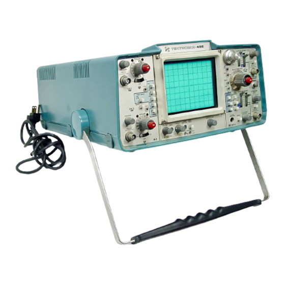
- Page 13 455/A2/B2 4 5 5 /A 2 /B 2 Portable Oscilloscope.
- Page 14 Standard 455 oscilloscopes can be operated from nominal 116 volt or 232 volt, 48 to 440 Hz power lines. With Option 7, the 455 can be operated from 12 or 24 vo lt dc power sources (or the snap-on T ektronix 1106 Battery Pack). Option 7 Specifica...
- Page 15 Specifications—4 5 5 /A 2 /B 2 TABLE 1-1 (continued) Electrical (455 Main Module) Characteristics Performance Requirement Supplemental Inform ation SIGNAL OUTPUTS (continued) A Gate O utput Voltage Approxim ately 5.0 V positive-going pulse. O utput Resistance Approxim ately 500 f2.
- Page 16 12 shocks. TABLE 1-3 Physical Information Characteristic Weight 27.0 lbs (12.2 kg). 455/A2/B2 w ith Panel Cover, Modules, Accessories and Accessory Pouch 24.0 lbs (10.9 kg). W ithout Panel Cover, Accessories, and Accessory Pouch 34.2 lbs (15.5 kg). Domestic Shipping Weight Height 9.00 in.
- Page 17 Specifications—4 5 5 /A 2 /B 2 TABLE 1-3 (continued) Physical Characteristic Inform ation Width With Handle 13.65 in. (34.67 cm). W ithout Handle 12.50 in. (31.75 cm). Depth Including Panel Cover 19.50 in. (49.53 cm). Handle Extended 21.70 in. (55.19 cm). Transportation Meets the lim its of National Safe Transit Committee Test Procedure 1A w ith a 30-inch...
- Page 18 Specifications— 455/A2/B2 T A B LE 1-4 Electrical (A2 Vertical Module) Supplemental Inform ation Characteristic Performance Requirement Deflection Factor Calibrated Range 5 mV to 5 V /D IV in 10 steps: 1-2-5 sequence. Uncalibrated (VAR) Range Provides continuously variable deflec...
- Page 19 Specifications— 4 5 5 /A2/B2 TABLE 1-4 (continued) Electrical (A2 Vertical Module) Characteristic Supplemental Inform ation Performance Requirement Common-Mode Rejection Ratio A t least 10:1 at 10 MHz fo r common (ADD Mode w ith CH 2 Inverted) mode signals o f 6 div or less with GAIN adjusted fo r best CMRR at 50 kHz.
- Page 20 Specifications— 455/A2/B2 TABLE 1-5 Electrical (B2 Horizontal Module) Characteristic Performance Requirement Supplemental Information TRIGGERING Sensitivity (See Fig. 1-2) In EXT -r 10, m ultiply requirements by 10. AC Coupled 0.4 div internal or 50 mV external from 60 Hz to 10 MHz increasing to 1.5 div internal or 250 mV external at 50 MHz.
- Page 21 S pecifications-455/A 2/B 2 TABLE 1-5 (continued) Electrical (B2 Horizontal Module) Supplemental Information Performance Requirement Characteristics TRIGGERING (cont.) External Trigger Input Maximum Input 250 V DC + peak ac or 250 V p-p ac (1 Voltage kHz or less). 1 MJ2 w ithin 10%.
- Page 22 Specifications— 455/A2/B2 TABLE 1-5 (continued) Electrical (B2 Horizontal Module) Supplemental Inform ation Characteristics Performance Requirement H ORIZONTAL DEFLECTION SYSTEM (cont.) A t least 2.5:1. Variable Range (A only) 2.5 to 1 continuously variable between calibrated settings. Extends slowest A Sweep rate to at least 1.25 s/div.
- Page 23 Specifications— 4 5 5 /A 2 /B 2 TABLE 1-5 (continued) Electrical (B2 Horizontal Module) Characteristics Performance Requirement Supplemental Inform ation X-Y OPERATION X-Y Operation Extreme counterclockwise position o f T IM E /D IV switch. CH 2 or X-Y button of VERT MODE switch must be pushed.
- Page 24 The follow ing accessories have been selected from our catalog specifically fo r your instrument. They are listed as a convenience to help you meet yo u r measurement needs. For detailed inform ation and prices, refer to a Tektronix Products Catalog or contact your local Tektronix Field Representative.
- Page 25 Order..........1105 Battery Power Supply 1106 BATTERY PACK A convenient, snap-on battery power supply fo r oper ating the 455 Option 7 oscilloscopes. Order .......... 1106 Battery Pack MESH FILTER Improves Display Contrast. Order..............378-0726-01 1-12 REV.
- Page 26 Section 2— 455/A2/B2 OPERATING INSTRUCTIONS This instrument has a 3-wire cord w ith a 3-terminal polar O P E R A T IN G V O L T A G E ized plug fo r connection to the power source and safety- earth.
- Page 27 To make a plug in current loop, order Tektronix Part 012-0259- 00 and m o d ify i t b y replacing the 50 £2 resistor (inside) w ith a bare wire.
- Page 28 Operating Instructions— 455/A2/B2 A 2 V E R T IC A L M O D U L E NOTE (F IG . 2-3) Use o f a 10X probe, w ith o u t a scale-factor CH 1 or X and CH 2 or Y —Input connectors fo r appli...
- Page 29 Operating lnstructions-455/A2/B2 signals at sweep rates slower than 0.5 m s/d coupling the AC-GIMD-DC-Selects the method for sweep rates o f 0.5 m s/div o r faster, the chof input signal to the vertical input amplifier. ments become visible. Use the alternate moc faster sweep rates.
- Page 30 Operating Instructions— 4 55 /A2/B2 display is presented. If the indicator is not lit when B2 H O R IZ O N T A L M O D U L E operating in the single-sweep mode, single-sweep (F IG . 2-4) displays w ill not be presented u ntil the SGL SWP button is pushed to reset the sweep.
- Page 31 Operating Instructions— 4 5 5 /A 2/B 2 NORM: With the proper A TRIGGER LEVEL con HORIZ DISPLAY—Determines the mode o f operation trol setting, A sweep can be initiated by trigger sig fo r the horizontal deflection system. nals w ithin the frequency range set by the A COUPLING switch.
- Page 32 Operating Instructions— 455/A2/B2 A TRIGGER LE V E L— Selects the amplitude point on COUPLING—Determines the method used to couple the trigger signal at which the sweep is triggered. It is signals to the trigger generator circuit. usually adjusted fo r the desired display after trigger SOURCE, COUPLING, and SLOPE have been selected.
- Page 33 Operating Instructions—4 5 5 /A 2/B 2 BASIC A PPLIC A TIO N S AND M E A S U R E M E N T S Peak-to-Peak Amplitude Measurements 5. Set the AC-GND-DC switch to DC. If the waveform appears above the reference line, the voltage is positive.
- Page 34 Operating Instructions— 455/A2/B2 Example: 2. Set the VERT MODE switch to either CHOP or A LT . In general, CHOP is more suitable fo r low-frequency signals and the A L T position is more suitable fo r high- Assume a horizontal difference o f 0.6 division w ith a sweep rate o f 45°/division as shown in Fig.
- Page 35 Operating Instructions— 4 5 5 /A 2 /B 2 5. Measure the horizontal difference (in divisions) be Use the follow ing procedure to reduce or eliminate the tween corresponding points on the waveforms. line-frequency component: 1. Apply the signal to the CH 1 input connector. 6.
- Page 36 Operating Instructions— 455/A2/B2 Fig. 2-10. Tim e duration. Fig. 2-11. Risetime. 2. Adjust the vertical POSITION control so that the dis Example: play bottom just touches the 0% graticule line and the dis play top just touches the 100% graticule line (see Fig. 2-11).
- Page 37 Operating Instructions— 4 5 5 /A 2/B 2 B D ELAYED D IF F E R E N T IA L TIM E MEASURE MENTS. Use the follow ing procedure to make differential time measurements using the B Delayed mode. 1.
- Page 38 Operating Instructions— 455/A 2/B 2 5. Set the HORIZ DISPLAY switch to B D LY 'D . 2. With the D ELAY TIM E POS control, move the left edge o f the intensified zone to the left side o f the portion o f the A sweep display to be magnified.
- Page 39 Operating Instructions— 4 5 5 /A2/B2 NOTE M AG N IFIED SWEEP TRIGGERED AFTER D ELAY. A t high apparent magnification, the magnified-sweep-starts- In ab ility to intensify the desired p ortion o f after-delay method may produce too much jitte r. To elim i the A sweep display indicates the lack o f a nate the jitte r, operate B sweep (in the triggered after delay transition o f sufficient amplitude, in that...
- Page 40 Performance Check o f the the case, refer to the Options section(s) in this manual and 455/A2/B2. Specifications given fo r the equipment are the minimum necessary for accurate results. perform the necessary performance checks.
- Page 41 Performance Check—4 5 5 /A 2 /B 2 P R E L IM IN A R Y PROCEDURE SWEEP (cont) Perform following steps to place 455/A 2/B 2 into a basic X10 MAG out (off) operating mode before continuing w ith the Performance A TRIGGER HOLDOFF Check.
- Page 42 Performance Check— 455/A2/B2 PG506 OR E Q U IV A L E N T A M P L IT U D E C A L IB R A TO R D U A L -IN P U T 4 5 5 /A 2 /B 2...
- Page 43 Performance Check—4 5 5 /A 2 /B 2 4. TRIGGER VIEW GAIN 5. TRIGGER VIEW D E LA Y DIFFERENCE a. Set: VERT MODE CH 1 a. Set: A T IM E /D IV ,0 5 A SOURCE EXT ^ 1 0 X10 MAG in (on) ASLOPE...
- Page 44 Performance Check— 455/A2/B2 6. CASCADED SEN SITIVITY b. Set generator frequency to 20 MHz. VERT MODE CH 2 c. CHECK—Display amplitude is at least 3.5 divisions. CH 1 and CH 2 VO LTS/ 5 mV D IV 8. CH 2 BANDW IDTH CH 1 and CH 2 AC-GND- a.
- Page 45 Performance Check—4 5 5 /A 2/B 2 d. Set generator frequency to 50 kHz (reference) and LOW FREQUENCY TRIGGERING adjust output amplitude fo r 5 division display. A TIME/DIV 10 ms e. Set generator frequency to 50 MHz. B TIME/DIV 10 ms X I 0 MAG out (off)
- Page 46 Performance Check— 455/A2/B2 SG503 OR E Q U IV A L E N T SINE-W AVE G ENERATO R 4 5 5 /A 2 /B 2 T-CONNECTOR 1907-12 Fig. 3-5. Sine-wave generator test setup #2. h. CHECK—No stable display can be obtained w ith B and —...
- Page 47 Performance Check— 455/A2/B2 15. 50 kHz EXTERNAL TRIGGERING e. CHECK— Stable display can be obtained in both + and — positions of B SLOPE switch for LF REJ position a. Adjust generator output amplitude fo r 2.5 division of B COUPLING switch.
- Page 48 Performance Check— 455/A2/B2 b. Set generator frequency to 50 kHz and adjust output 18. 50 MHz INTERNAL TRIGGERING amplitude for 5 division display. a. Set: HORIZ DISPLAY A and B SOURCE NORM c. Disconnect 50 SI cable and term ination from dual...
- Page 49 Performance Check—4 5 5 /A 2 /B 2 j. CHECK—Display is triggered along negative-going NOTE slope o f waveform as B LEVEL control is rotated and is I f the 11th time marker is n o t visible, set the A not triggered (not visible) at either extreme o f B LEVEL T IM E /D IV switch one position counterclock...
- Page 50 Performance Check— 455/A2/B2 TABLE 3-3 (continued) TABLE 3-4 A and B Timing Accuracy A and B Magnified Accuracy A and B Time-Mark Portions of Total T IM E /D IV Generator Magnified Sweep A and B Time-Mark Switch Setting Output...
- Page 51 Performance Check— 455/A2/B2 d. Set D ELAY TIM E POS (DTP) control to 9.00. Then TABLE 3-5 move DTP to position 1st displayed marker to graticule Differential Time Accuracy vertical centerline. Time-Mark A T IM E /D IV B T IM E /D IV...
- Page 52 Performance Check— 455/A2/B2 27. CALIBR ATO R OUTPUT d. Disconnect test oscilloscope. a. Set: CH 1 V O LTS/D IV .1 V A T IM E /D IV .5 ms 26. CHOPPED MODE REP RATE a. Set VERT MODE to CHOP and set A LEVE L for b.
- Page 53 O R P E R F O R M A N Y S E R V I C I N G U N L E S S Q U A L I F I E D TO D O SO. This section describes the circuitry used in the 455/A2/B2 Oscilloscope. The description begins w ith a discussion o f the basic circuit functions o f each module, then expands into a detailed description of the individual circuits.
- Page 54 Circuit Description— 4 5 5 /A2/B2 A trigger pickoff stage in each Preamplifier circuit provides voltage powering the instrument. Each trigger circuit con a sample of the Channel 1 and Channel 2 input signals to the tains LEVEL, SLOPE, COUPLING and SOURCE controls. Horizontal Module fo r sweep triggering purposes.
- Page 55 Main Module drive tw o single-ended at about 0 volt. To make a plug-in current loop, order Tektronix Part 012-0259-00 and modify it by replacing the 50 resistor (inside) with a bare wire. A current loop also can be made from 5 turns of insulated wire.
- Page 56 Circuit Description— 4 5 5 /A 2/B 2 Diode CR358 protects the Sweep Gate Am plifier in the The feedback voltage again reaches a level which turns on event that greater than +5 volts is applied to the + GATE Q552.
- Page 57 Circuit Description— 455/A2/B2 more negative charge. The more negative the voltage across Transistors Q518, Q526, and Q524 compose a feedback amplifier stage, with R515 and R516 as the feedback elements. C548, the later Q552 turns on. See Figure 4-1 showing Capacitors C515and C516 provide high-frequency compensa...
- Page 58 Circuit Description— 455 /A 2 /B 2 changing from one line voltage to the other, the line fuse Fuses F736, F746 and F768 provide short-circuit protection fo r each o f the unregulated supplies. should be changed as follows: 1 amp fast blow fo r 116 volts or 0.5 amp fast blow fo r 232 volts.
- Page 59 Circuit D escription-455/A2/B2 The effective overall deflection factor of each channel is CHANNEL 1 A N D CHANNEL 2 determined by the VO LTS/D IV switch setting. The basic INPUT CIRCUITS deflection factor of the vertical deflection system is 5 m V / div.
- Page 60 Circuit Description— 4 55 /A2/B2 Fig. 4-3. Attenuator and gain switching sequences. REV. A, OCT 1975...
- Page 61 Circuit Description— 455/A2/B2 Fig. 4-4. Channel switching gates. REV. A, OCT 1975...
- Page 62 Circuit Description— 4 5 5 /A2/B2 PREAMPLIFIERS. The Channel 1 input signal from the In the A L T mode, the Alternate Trace Sync Pulse Am plifier FET Input Source Follower enters terminal 1 of the HIC; is turned on, allowing the pulses to switch the multivibrator. Channel 2 signal enters at terminal 32.
- Page 63 Circuit Description— 455/A2/B2 V E R T IC A L OUTPUT A M P LIFIE R Resistors R4386, and 75 £2 line termination (Horizontal Module) divide the signal at the emitter of Q4384 to the The Vertical O utput Am plifier circuit provides the final appropriate signal level fo r the trigger.
- Page 64 Circuit Description— 4 5 5/A 2/B 2 TRIG G ER INPUT Input Source Follower Field effect transistors Q2120A and Q2170A are source This circuit determines triggering source and coupling and, followers. They provide high input impedance fo r the through source follower stages, presents trigger signals to the trigger signals and also provide isolation between the trigger Trigger Generator circuit.
- Page 65 Circuit Description— 455/A2/B2 Pin 9. Free run in. (Used on B sweep only.) Controls Pin 14. Not connected internally. the state of the Sweep Gate output at pin 10. When pin 9 is HI (STARTS AFTER DELAY mode) pin 10 is LO.
- Page 67 Circuit Description— 4 55/A2/B2 Pin 6. Start Level Current Input. Sets current levels in The Sweep Gate output at pin 10 steps LO to trigger the the diodes which determine the sweep start voltage. sweep. The Logic Gate output at pin 11 is identical to pin 10 and is used to trigger Sweep Control circuit functions.
- Page 68 Circuit Description— 4 5 5 /A2/B2 When both pins 13 and 14 o f U2790 are LO, the Sweep Pin 2. Single sweep reset. Pushing the SGL SWP push Start Comparator (inside U2790) minus input is pulled LO. button resets the sweep triggering circuit, making it This causes pin 4 of the 1C to become a high impedance, ready fo r another single sweep to be triggered.
- Page 69 Circuit Description— 455/A2/B2 A Sweep Mode Pin 13. Triggered light. Voltage at this pin lights the TRIG light when a triggered gate has occurred. Assuming a triggerable signal is applied to pin 2 o f U2700, gate pulses are produced at pin 10 and 11 (see Fig. 4-8 and 4-9).
- Page 70 Circuit D escription-455/A 2/B 2 until a trigger signal occurs at pin 2 of U2600. When the B B Dly'd Sweep Mode sweep starts, a crt unblanking signal is produced at pin 12 In the B D LY'D mode. Fig. 4-10, the A sweep operates of U2690 to unblank the crt.
- Page 71 Circuit Description— 4 55 /A2/B2 Horizontal Preamplifier 1C The Horizontal Preamplifier circuit is contained w ithin a single 1C, U2900. The following is a brief description of the function associat ed w ith each pin of U2900. Pin 1. Magnifier registration. This pin is used in con junction w ith pin 8 to provide registration between the normal and magnified sweeps.
- Page 72 Circuit Description— 45 5 /A 2/B 2 S2100 S2650 1 9 0 7 - 3 9 Fig. 4-10. Sweep operation in B D L Y 'D mode. REV. A, OCT 1975 4-20...
- Page 73 Section 5 -4 5 5 /A2/B2 MAINTENANCE This section contains information fo r use in preventive or corrective maintenance. The corrective maintenance portion includes information on component removal and replacement. CABINET REMOVAL W A R N I N G Dangerous potentials exist a t several points inside this instrument. To prevent electrical shock, do n o t touch exposed connections o r components when the instrument is operated with the cabinet removed.
- Page 74 Mai ntenance— 4 5 5 /A 2 /B 2 2. Greasy residues or dried-on d irt can be removed w ith A void the use o f chemical cleaning agents which solution of warm water and neutral pH liquid detergent. m ight damage the plastics used in this instrument.
- Page 75 Tektronix, Inc. Order all special parts directly from your local Tektronix Field Office or representative. 3. Bend leads of new component to f it holes in board. If component is replaced while board is mounted in instru...
- Page 76 Maintenance— 4 5 5 /A2/B2 COMPONENT REM O VAL AND REPLACEMENT To install the rear panel assembly, set the bottom of the subpanel into the groove in the cabinet bottom and in stall the four screws. Be sure to reconnect all intercon necting cables.
- Page 77 Maintenance— 4 55 /A2/B2 3. Bend grooved part of holder so that connector is inserted individual items, but if the connectors are faulty, the entire into groove. cable should be replaced. When plugging connector holders on to board pins, be sure It is possible for the pin connectors to become dislodged to match triangle mark on holder with triangle mark on from the plastic holders.
- Page 78 Maintenance— 455/A2/B2 2. Remove plastic bezel and filte r from front of crt (held RETAINER: with 4 screws). BUSHING : 3. Unplug crt anode lead and discharge to chassis. 4. Unplug c rt base socket. RECESSED PORTION OF SHAFT 5. Disconnect 2 vertical deflection plate leads from left side of c rt neck.
- Page 79 Maintenance— 4 55 /A2/B2 TO REMOVE MODULE SCREW VERTICAL DEFLECTION PULL STRAIGHT UP PLATE LEAD UPPER WHITE-BLUE 1907-43 Fig. 5-5. Vertical Module removal. Refer to Fig. 5-6 when replacing the LED's. Use a low- Vertical Module Removal (Fig. 5-5) wattage soldering iron and apply only enough heat to solder To remove module: the LED leads to the etched circuit cable.
- Page 80 Maintenance— 4 5 5 /A2/B2 BOTTOM FRAME Fig. 5-7. V O L T S /D IV switch disassembly. REV. A, OCT 1975...
- Page 81 Maintenance- 4 5 5 /A2/B2 If disassembly is necessary, read the following list of special V O LTS /D IV Switch Assembly Removal considerations before beginning disassembly (see Fig. 5-7). To remove switch assembly: 1. Remove VAR knob using hex wrench. Substrate or Contact Replacement Considerations 1.
- Page 82 Maintenance— 4 5 5 /A 2 /B 2 Hybrid 1C Removal 2. Carefully lift clamp and hybrid 1C from socket. Be careful not to damage socket contacts. To install hybrid 1C: Handle h y b rid 1C carefully. Ceramic material m ay break i f dropped.
- Page 83 Maintenance— 455/A2/B2 SCREW TO REMOVE MODULE PULL STRAIGHT AWAY FROM MAIN MODULE INTERFACE CONNECTOR POWER SWITCH EXTENSION ROD SNAPS INTO PLASTIC RETAINER ON POWER SWITCH 1907-47 Fig. 5-9. Horizontal Module removal. Horizontal Module Removal (Fig. 5-9) To remove module: 1. Remove tw o screws holding module.
- Page 84 Maintenance— 4 5 5 /A 2 /B 2 A and B Timing Switch Board Removal To remove switch assembly: D o n o t touch switch contacts; they can be easily damaged o r contam inated. I f cleaning is neces sary, use a s o ft camel-hair brush and isopropyl 1.
- Page 85 Mai ntenance— 4 5 5 /A2/B2 5. Rotate both outer (A) and inner (B) shafts to .2 jus 2. Remove POSITION, LEVEL, and A TRIGGER HOLD- position (third position from fu lly clockwise). OFF knobs. See shaft-knob removal procedure in this section.
- Page 86 The compo nent number and electrical value of each component in this Example: Tektronix 576 Curve Tracer or Tektronix 577 instrument are shown on the diagrams (see the first page of (D 1 or D2) Curve Tracer with 177 Test Fixture.
- Page 87 Maintenance— 455/A2/B2 © TOLERANCE; F=±1%, J=5%, K=10%, M=20% ( a ) COLORS IDENTIFY SIGNIFICANT DIGITS IN TEKTRONIX PART NUMBER (E.G. BROWN, GRAY, GREEN STRIPES INDICATE PART NUMBER 152-0185-00) © (TCJ © and © 1ST, 2ND, AND 3RD SIGNIFICANT FIGS. AND/OR COLOR CODE MAY NOT BE PRESENT ON SOME CAPACITORS;...
- Page 88 5. Module Extender Troubleshooting fixture Supply Tolerance Ripple (peak-to-peak) Description: 18 inch ribbon cable with a module inter face connector at each end (Tektronix part 067-0757-00). - 5 V + 1.1% (5.5 mV) 1 mV Purpose: To operate Vertical and Horizontal modules +5 V ±1.1% (5.5 mV)
- Page 89 ATTENUATORS. The th ick film attenuators are best reverse biased, while the enhanced mode has the junction checked by substitution. If only one channel o f the 455 is forward biased. not operating properly, and there is reason to believe an...
- Page 90 Maintenance— 4 5 5 /A 2/B 2 Fig. 5-13. Troubleshooting chart. 5-18 REV. A, O C T 1975...
- Page 91 Maintenance— 4 5 5 /A2/B2 1907-1 A Fig. 5-13. Troubleshooting chart (cont). REV. A, O C T 1975 5-19...
- Page 92 REPACKAGING FOR SHIPMENT protect the finish of the instrument. If the Tektronix instrument is to be shipped to a Tektronix 3. Cushion the instrument on all sides by tightly packing Service Center fo r service or repair, attach a tag showing: dunnage or urethane foam between carton and instru...
- Page 93 Section 6— 455/A2/B2 ADJUSTMENTS IMPORTANT-PLEASE READ BEFORE USING THIS PROCEDURE The purpose o f this procedure is to provide an adjustment sequence that w ill allow an operating instrument to be adjusted to meet its original performance requirements; it is not intended as a troubleshooting guide. Any trouble which becomes appar...
- Page 94 1 ns or less from compensation adjust Generator1. the fast-rise output; output ments. amplitude, 60 V from high- b. Tektronix Type 106 Square- amplitude output; aberrations, Wave Generator. w ithin 2% from fast-rise output. 5. Sine-Wave Generator Frequency, 50 kHz to above Vertical bandwidth a.
- Page 95 Adjustments— 455/A2/B2 A. M A IN MODULE Equipment Required 5. 50 Termination 1. Digital Voltmeter 2. Time-Mark Generator 6. Low-Capacitance Screwdriver 3. Test Oscilloscope 7. Screwdriver 4. 50 £2 Cable P R E LIM IN A R Y PROCEDURE A COUPLING...
- Page 96 Adjustments—455/A 2 /B 2 d. Set FOCUS and ASTIG controls fo r well-defined spot. If spot is not displayed, adjust Crt Bias adjustment, R532, (see Fig. 6-3) fo r a visible spot. Then, adjust FOCUS and ASTIG controls. e. ADJUST— Crt Bias, R532, counterclockwise until spot is just barely visible.
- Page 97 Adjustments— 455/A2/B2 c. Set A T IM E /D IV and VAR TIM E /D IV controls to obtain exactly one time mark/division (may be neces sary to set A T IM E /D IV to .5 ms). d. A D JU S T -Y AXIS, R573 (see Fig. 6-3), to align center time mark with center vertical graticule line.
- Page 98 Adjustments— 4 5 5 /A2/B2 B. V E R TIC A L MODULE Equipment Required 1. Amplitude Calibrator 7. 20 pF BNC Normalizer 2. Square-Wave Generator 8. Alignment Tool 3. Sine-Wave Generator 9. Low-Capacitance Screwdriver 4. 50 £2 BNC Cable 10.
- Page 99 Adjustments— 455/A2/B2 b. Set: CH 2 VO LTS/DIV 5 mV d. Set VERT MODE to CH 2. A T IM E /D IV .05 jus ASLOPE O U T: + e. Move 20 mV amplitude-calibrator signal to CH 2 input connector.
- Page 100 Adjustments— 455/A2/B2 g. Increase generator frequency to 50 MHz. Display BG. BANDWIDTH CHECK amplitude should be at least 4.2 divisions. a. Set VERT MODE to CH 1. N O TE b. Connect sine-wave generator output to CH 1 input via 50 El cable and 10X attenuator.
- Page 101 A-PDF Solit DEMO : Purchase from www.A-PDF.com to remove the watermark______ -----------------K------------------------------------------------------ — --------------------------------------------------- AdjU5tments-455/A2/B2 Fig. 64. Vertical adjustment locations. REV. B, MAY, 1976...
- Page 102 Adjustments— 4 5 5 /A 2/B 2 C. HO R IZO N TA L MODULE Equipment Required 1. Time-Mark Generator 5. 50 £2 Termination 2. Sine-Wave Generator 6. Low-Capacitance Screwdriver 3. Am plitude Calibrator 7. Screwdriver 4. 50 £2 Cable b.
- Page 103 Adjustments— 455/A2/B2 C2. HORIZONTAL GAIN f. INTERACTION—Due to interaction between R2782 and R2748, repeat steps b through e several times until a. Set HORIZ DISPLAY to A. Center display. no further adjustment is necessary. b. ADJUST— X I Gain, R2923 (see Fig. 6-6), fo r one major time mark/division.
- Page 104 Adjustment—4 5 5 /A 2/B 2 C4. B START LEVEL e. ADJUST— C2684 (see Fig. 6-5) fo r 1 tim e mark/ division. a. Set: B T IM E /D IV 1 ms X10 MAG in (on) Set: B TIM E /D IV ,0 5 /is(p u ll to unlock DELAY TIME POS...
- Page 105 Adjustments— 455/A2/B2 c. Center display with horizontal POSITION. c. Set controls to display 6 divisions, 3 divisions above and 3 divisions below graticule horizontal centerline. d. Set X10 MAG pushbutton in (on). d. ADJUST— A Trigger Level Centering R2715 (see Fig.
- Page 106 OPTION 7 Permits the 455 to be powered from a dc source of 12 volts or 24 volts in addition to the standard ac line operation. For battery operation. Option 7 makes the 455 compatible w ith the Tektronix 1106 Battery Pack.
- Page 107 Instrument Options— 455/A2/B2 OPTION 4 The 455 Option 4 oscilloscope is modified to meet the EMC requirements of MIL-STD-461A when tested in accordance with the following test methods of MIL-STD-462: CE-01, CE-03, CS-01, CS-02, CS-06, RE-02 (limited to 1 GHz), (T) RE-04, RS-01, and RS-03 (limited to 1 GHz).
- Page 108 Instrument Options—455/A2/B2 O PTIO N 4 REPLACEABLE ELECTRICAL PARTS Tektronix Serial/M odel No. Ckt No Part No. Dscont Name & Description Code M fr Part Number C707 283-0110-00 CAP. ,FXD.CER DI: 0.005UF,+80-20%,150V 19C242B 56289 C708 283-0003-00 CAP. ,FXD,CER DI:0.01UF,+80-20%,150V 72982...
- Page 109 Instrument Options— 455/A2/B2 OPTION 5 Option 5 adds a sync separator which provides additional processing fo r trigger signals to facilitate observation of composite video and related television waveforms. Added circuitry provides amplification, selectable polarity inversion, clipping, and sync recognition. The output o f this circuitry supplies both vertical (field-rate) and horizontal (line-rate) trigger signals to the A TRIGGER COUPLING switch and supplies horizontal (line-rate) trigger signals to the B (D LY'D ) TRIGGER SOURCE switch.
- Page 110 Instrument Options— 4 5 5 /A 2 /B 2 OPERATING IN F O R M A T IO N Typical operation of an Option 5 instrument uses A sweep to establish a basic field and frame-related display. Then, all detail measurements are made using B Sweep.
- Page 111 Instrument Options-455/A2/B2 4. Set the HORIZ DISPLAY switch to B D LY'D . This signal addition and therefore are not affected by addition. displays the portion of the A Sweep display that was The normal trigger signal is picked o ff after signal addition intensified.
- Page 112 Instrument Options— 455/A2/B2 3. Set the X I 0 MAG button to the in position and horizon horizontal sync pulse. The Field 1 picture starts w ith a full ta lly position the display desired. This provides sufficient line of video.
- Page 113 Instrument Options—455/A 2/B 2 Field which follows a field ending in a full line Field 2: of line 313. Burst starts on line 6 (immediately which does not carry color burst. Field 2 lines are following the last equalizing pulse); a half-line of the last half of line 313 through line 625.
- Page 114 B2 Option 5: A SOURCE NORM B SOURCE TV LINE 1. Television Test Signal Generator, Tektronix part 067- 0601-00. 2. Install 405/50 Program Card into Television Test Generator. 2. 405/50 Program Card, Tektronix part 067-5001-00.
- Page 115 Instrument Options— 455/A2/B2 c. CHECK— Stable display w ith intensified portion at d. Adjust A TRIG HOLDOFF until jitte r stops. start of sweep can be obtained by adjusting the B LEVEL control. e. Set: X10 MAG out (off) d. Set HORIZ DISPLAY to B DLY'D.
- Page 116 Instrument O p tio n $ -4 5 5 /A 2 /B 2 CIRCUIT DESCRIPTION BLOCK D IA G R A M SW ITCHING Setting the A COUPLING switch to T V LINE or T V FIELD In the AC, LF REJ, HF REJ, and DC positions o f the activates the sync separator circu it (see Fig.
- Page 117 Instrument Options— 455/A2/B2 The input signal is supplied to both the inverting and non The output of the sync-separator circuit is supplied to the A and B trigger generators via the A COUPLING and B inverting inputs of the operational amplifier through 2 voltage dividers.
- Page 118 Instrument Options—4 5 5/A 2/B 2 V E R T IC A L SYNC RECOGNIZER the emitter o f U2232D goes positive enough to overcome the charge on C2242, a positive-going signal is supplied to the base o f U2218E through emitter follower Q2246. This The negative-sync output at the collector of U2218B is applied causes U2218E to conduct through CR2245 and help charge to the input of the Vertical Sync Recognizer composed of...
- Page 119 Instrument Options— 455/A2/B2 VOLTAGE CONDITIONS Voltages shown on this schematic diagram were measured with a Tektronix DM 501 Digital Multimeter. Voltage measurements can vary as much as ±20%. The B2 A COUPLING switch was set in the FIELD position. WAVEFORM CONDITIONS Waveforms below were taken from a Tektronix 7000-series oscilloscope equipped with readout, 7B series time-base, 7A13 Differential comparator and a 10X probe.
- Page 120 Instrument Options— 455/A2/B2 > o j a. < O R E V . B, APR. 1977 Option 5 Page 12...
- Page 121 Instrument 455/A2/B2 Options— G R ID G R ID G R ID G R ID G R ID G R ID G R ID C2105 CR2104 TP2125 Q2212 R2135 R2233 R2257 C2113 CR2108 R2164 R2234 R2258 TP2238 Q2236 C2114 R2261...
- Page 122 Instrument Options—455/A2/B2 O P TIO N 5 REPLACEABLE PARTS ABBREVIATIONS IN C H E L E C T R O N S IN G L E E N D I N C H e l c t r n I N C A N D...
- Page 123 Instrument Options— 455/A 2/B 2 Tektronix Serial/Model No. Ckt No. Part No. Dscont Name & Description Code Mfr Part Number R2212 315-0105-00 RES. ,FXD,CMPSN:1M 0HM,5%,0.25W 01121 CB1055 R2213 315-0272-00 RES. . , FXD,CMPSN:2.7K 0HM,5%,0.25W 01121 CB2725 R2214 RES. ,FXD,CMPSN:15K OHM,5%,0.25W...
- Page 124 Instrument Options—455/A2/B2 „ REPLACEABLE M ECHANICAL PARTS Fig. & M fr Index Tektro n ix S e ria l/M o d e l No. Code M fr Part Num ber Part No. Dscont 1 2 3 4 5 N am e & Description...
- Page 125 OPTION 7 Option 7 permits the Tektronix 455 oscilloscope to be powered from a dc source o f 12 volts or 24 volts in addition to the standard ac line operation. For battery operation. Option 7 makes the 455 compatible w ith the Tektronix 1106 Battery Pack.
- Page 126 Instrument O ption$-455/A 2/B 2 Fig. Option 7-2. Dc voltage selector switch and dc input connector. TABLE 1 Option 7 Power Sources Oscilloscope POWER Power Source Voltage Selectors Switch 115 V A C 116 V 230 V AC 232 V...
- Page 127 Instrument Options—455/A2/B2 C IR C U IT D ESC R IP TIO N Option 7 consists basically o f a dc to ac inverter that operates on 12 or.24 volts. The circuit description discusses 24 volt oper ation unless noted otherwise. Refer to the schematic diagrams fo r additional details.
- Page 128 Instrument Options— 455/A2/B2 Inverter Circuit the bridge rectifier. Capacitor C612 prevents Q622 from turning on when the inverter is started, allowing the power The Start current is applied to the base of Q662 and Q666 source time to recover after providing the initial start surge.
- Page 129 3. A description of the part (if electrical, include nents are manufactured or selected by T ektronix, Inc. to the circuit number). meet specific performance requirements, or are manufac tured for Tektronix, Inc. in accordance w ith our specifica 4. Tektronix part number. ADJUSTMENTS Equipment Required a.
- Page 130 Instrument Options— 4 5 5 /A 2/B 2 ADJUSTM ENT PROCEDURE a. Operate the oscilloscope in the 24 V mode. 1. OPERATING RANGE b. Set the variable power supply output fo r 24 V. a. Connect the dc source to the oscilloscope equipped with Option 7.
- Page 131 Waveforms may vary as much as ±20%. The 455 was powered from a 24 V dc source. The IN T E N S IT Y control was set for normal trace brightness or about midrange. The test oscilloscope was externally triggered using the waveform at the collector of Q 662.
- Page 132 Instrument Options— 455/A2/B2 Option 7 Page 8 REV E A UG 1979...
- Page 133 Instrument Options— 455/A2/B2 CRGfi2 CRG66 ■ {TO5T1 R632 ] CR832 ■ > j W N V W ' W ; CRB33 . ■ ■ m wn. •, C60U CR638 R63S : CR639 R638 rtv\ • \SW\N\ \WW AWS\\vv\» \\ W W V...
- Page 134 Instrument Options—455/A2/B2 O P T IO N 7 REPLACEABLE ELECTRICAL PARTS Tektronix Serial/ Model No. Name & Description Code M fr Part Number Dscont Ckt No. Part No. CAP.,FXD,CER DI:0.0022UF,20%,3000V 56289 33C319 C700 283-0263-00 CAP. ,FXD,CER DI.-0.0022UF,20%, 3000V 56289 33C319...
- Page 135 Instrument Options—455/A2/B2 Tektronix Serial/M odel No. Ckt No. Part No. Dscont Name Description Code Mfr Part Number & Q652 S038487 151-0302-00 07263 TRANSISTOR:SILICON,NPN Q656 SJE917 151-0335-00 TRANSISTOR SILICON,PNP 04713 Q662 151-0436-00 B010100 80009 151-0436-00 BO 33249 TRANSISTOR:SILICON,NPN Q662 153-0636-00 80009...
- Page 136 Instrument Options—455/A2/B2 REPLACEABLE MECHANICAL PARTS Fig. & Tektronix Serial/Model No. Index Mfr Part Number Part No. Dscont Qty 1 2 3 4 5 Name & Description Code 105-0695-00 l ACTR ASSY,SW:POWER 105-0695-00 80009 (REPLACES EXISTING PART IN STANDARD INSTRUMENT) 358-0560-00 l BUSHING,SLEEVE:0.254 ID,PLASTIC,0.34 OD...
- Page 137 Instrument Options—455/A2/B2 Fig. & Tektronix Serial/Model No. Index Mfr Part Number Code Dscont Qty 1 2 3 4 5 Name Description & Part No. 75915 357001 BO 10100 B057349X . FUSEHOLDER:3AG FUSE 352-0031-00 . (HOLDER FOR F600 DELETED AT S/N B057350 & C601 .
- Page 138 Instrument Options— 455/A2/B2 OPTION 78 This option adds a Type P11 phosphor CRT to the If this option is being added to an instrument which is instrument. already equipped w ith a different phosphor, or if the cathode-ray tube requires replacement, use the following...
- Page 139 ELECTRICAL PARTS PARTS ORDERING INFO RM ATIO N Replacement parts are available from o rth ro u gh your local Tektronix, Inc. Field O ffice or representative. Changes to Tektronix instrum ents are sometimes made to accomm odate im proved com ponents as they become available, and to give you the benefit of the latest circu it improvements developed in our engineering department.
- Page 140 Replaceable Electrical Parts— 455/A 2/B 2 CROSS IN D E X -M F R . CODE NUMBER TO MANUFACTURER City, State, Zip Mfr. Code Manufacturer Address 00853 SANGAMO ELECTRIC CO., S. CAROLINA DIV. P 0 BOX 128 PICKENS, SC 29671...
- Page 141 Replaceable Electrical Parts— 455/A2/B2 Tektronix Serial/M odel No. Mfr Part Number Name & Description Code Part No. Dscont Ckt No. 670-3555-00 B033529 CKT BOARD ASSY:INTERFACE 80009 670-3555-00 B010100 670-3555-01 B049999 CKT BOARD ASSY:INTERFACE 80009 670-3555-01 B033530 670-3555-02 80009 B068539 CKT BOARD ASSY:INTERFACE...
- Page 142 Replaceable Electrical Parts—455/A2/B2 Tektronix Serial/M odel No. Ckt No. Code M ir Part Number Part No. Dscont Name Description & C288 8005D9AABZ5U104M 281-0775-00 CAP. . , FXD,CER DI:0.1UF,20%,50V 72982 C354 56289 19C611 283-0080-00 CAP. , , FXD,CER DI:0.022UF,+80-20%,25V C376 19396...
- Page 143 Replaceable Electrical Parts— 455/A2/B2 Tektronix Serial/M odel No. Code Mfr Part Number Ckt No. Part No. Name & Description Dscont C2105 281-0773-00 CAP.,FXD,CER DI:0.01UF,10%,100V 72982 8005H9AADW5R103K C2113 281-0774-00 CAP.,FXD,CER DI:0.022UF,20%,100V 72982 8045A9ABDZ5U223M C2114 281-0759-00 CAP.,FXD, CER DI:22PF,10%,100V 72982 8035D9AADC1G220K C2115 281-0766-00 CAP.,FXD,CER DI:100PF,20%,200V...
- Page 144 Replaceable Electrical Parts—455/A2/B2 Tektronix Serial/M o del No. Ckt No. Part No. Dscont Name & Description Code Mfr Part Number C2781 290-0267-00 CAP. ,FXD,ELCTLT:1UF,20%,35V 56289 162D105X0035CD2 C2783 283-0126-00 B010100 B044699 CAP. ,FXD,CER DI:82PF,5%,1000V 56289 33C180 C2783 281-0816-00 B044700 CAP. ,FXD,CER DI:82PF,5%,100V...
- Page 145 Replaceable Electrical Parts— 455/A2/B2 Tektronix Serial/M odel No. Name Description Code Mfr Part Number Ckt No. Part No. Dscont & C4192 CAP. ,,FXD,ELCTLT:6.8UF,20%,35V 56289 196D685X0035KA1 290-0517-00 C4200A CAP.,,FXD,PLSTC:0.019UF,10%,600V 80009 285-0816-01 285-0816-01 (FURNISHED AS A UNIT WITH A4200) CAP...VAR.CER DI:1.2-10.2PF,400V 80031...
- Page 146 Replaceable Electrical Parts— 455/A 2/B 2 Tektronix Serial/M odel No. Ckt No. Part No. Dscont Name Description Code Mfr Part Number & C4414 281-0625-00 B030000 CAP. , FXD,, CER DI:35PF,5%,500V 72982 308-000C0G0350J C4417 281-0208-00 CAP., VAR PLSTC:5.5-50PF,100V 80031 2810C5R5506H02F0 C4418...
- Page 147 Replaceable Electrical Parts— 455/A2/B2 Tektronix S e r i a l / M o d e l No. M fr Part No. Dscont N am e & Description Code M fr Pa Cktjsjo^ SEMICOND DEVICE:SILICON,200V,I500MA '-0488-00 04713 3N55 FAMILY CR721...
- Page 148 Replaceable Electrical Parts— 455/A2/B2 Serial/Model No. Tektronix Name Description Code Mfr Part Number & Dscont Ckt No. Part No. 53184 LT EMITTING DIO:RED,650NM.40MA MAX XC209R B056950 CR4115 150-1031-00 01295 TIL 209A LAMP,LED:RED,3.OV, 40MA B056949 CR4117 150-1036-00 B010100 LT EMITTING DIO:RED,650NM.40MA MAX...
- Page 149 Replaceable Electrical Parts— 455/A 2/B 2 Tektronix Serial/M o del No. Part No. Dscont Name Description Mfr Part Nur Ckt No. Code & J600 (SEE OPTION SECTION 7 FOR PART NUMBER 6 VALUE) J2100 131-0352-02 CONNECTOR,RCPT,:BNC,FEMALE 24931 28JR166-1 J2150 131-0352-02...
- Page 150 Replaceable Electrical Parts— 455/A2/B2 Tektronix Serial/Model No. Ckt No. Part No. Dscont Name & Description Code Mfr Part Number Q764 151-0301-00 TRANSISTOR:SILICON,PNP 04713 2N2907A Q766 151-0301-00 2N2907A TRANSISTOR:SILICON,PNP 04713 Q768 151-0349-00 TRANSISTOR:SILICON,NPN,SEL FROM MJE2801 SJE924 04713 Q784 151-0405-00 TRANSISTOR:SILICON,NPN,SEL FROM MJE800...
- Page 151 Replaceable Electrical Parts— 455/A 2/B 2 Serial/Model No. Tektronix Code Mfr Part Number Name & Description Ckt No. Part No. Dscont 01121 CB4705 RES. ,FXD, CMPSN:47 OHM,5%,0.25W R246 315-0470-00 CB1015 RES . , FXD, CMPSN:100 OHM,5%,0.25W Oil 21 R247 315-0101-00...
- Page 152 Replaceable Electrical Parts— 455/A2/B2 Tektronix Serial/Model No. Ckt No. Name & Description Code Mfr Part Number Part No. Dscont R548 315-0101-00 RES.,FXD,CMPSN:100 OHM,5%,0.25W 01121 CB1015 R553 315-0101-00 RES.,FXD,CMPSN:100 OHM,5%,0.25W 01121 CB1015 R554 315-0120-00 RES.,FXD,CMPSN:12 OHM,5%,0.25W 01121 CB1205 R556 315-0511-00 RES.,FXD,CMPSN:510 OHM,5%,0.25W...
- Page 153 Replaceable Electrical Parts— 455/A 2/B 2 Tektronix Serial Model No. Mfr Part Number Ckt No. Part No. Dscont Name Description Code & 91637 MFF1816D50000C R742 321-0816-03 RES..,FXD,FILM:5K OHM,0.25%,0.125W 01121 CB4325 R743 315-0432-00 RES..,FXD,CMPSN:4.3K OHM,5%,0.25W 01121 CB1535 R745 315-0153-00 RES..,FXD,CMPSN:15K OHM,5%,0.25W...
- Page 154 Replaceable Electrical Parts— 4 55/A2/B2 Tektronix S eria l/M o del No. Ckt No. Part No. Dscont Name & Description Code Mfr Part Numbe R2176 315-0180-00 RES.,FXD,CMPSN:18 OHM,5%,0.25W 01121 CB1805 R2177 315-0470-00 RES.,FXD,CMPSN:47 OHM,5%,0.25W 01121 CB4705 R2212 ---------- (SEE OPTION SECTION 5 FOR PART NUMBER &...
- Page 155 Replaceable Electrical Parts— 455/A 2/B 2 Tektronix Serial/Model No. Code Mfr Part Number Name & Description Ckt No. Part No. Dscont 73138 R2682 RES. ,VAR,NONWIR:10K OHM,20%,0.50W 91-81-0 311-1559-00 RES. ,FXD,CMPSN: 47K OHM,5%,0.25W 01121 CB4735 R2683 315-0473-00 01121 CB3035 R2684 RES. ,FXD,CMPSN:30K OHM,5%,0.25W...
- Page 156 Replaceable Electrical Parts—455/A2/B2 T e k t r o n i x M f r S e r i a l / M o d e l No. C k t No. P a r t No. D s c o n t...
- Page 157 Replaceable Electrical Parts—455/A2/B2 Tektronix Serial/Model No. Ckt No. Part No. Dscont Name & Description Code Mfr Part Number RES. ,FXD, CMPSN:13K OHM,5%,0.25W 315-0133-00 01121 CB1335 R31 32 315-0913-00 RES. ,FXD,CMPSN:91K OHM,5%,0.25W 01121 CB9135 R3133 315-0223-00 RES. ,FXD,CMPSN:22K OHM,5%,0.25W 01121 CB2235...
- Page 158 Replaceable Electrical Parts— 455/A2/B2 T ektro n ix S e r i a l / M o d e l No. Ckt No. Part No. Dscont N am e & Description Code Mfr Part Number R4156 315-0101-00 RES.,FXD, CMPSN:100 OHM,5%,0.25W...
- Page 159 Replaceable Electrical Parts—455/A2/B2 Serial/M odel No. Tektronix Code Mfr Part Number Name Description Dscont Ckt No. Part No. & 01121 CB1625 RES. ,FXD,CMPSN:1.6K OHM,5%,0.25W B010610 R4254 315-0162-00 01121 CB1015 RES. ,FXD,CMPSN:100 OHM,5%,0.25W R4256 315-0101-00 (FURNISHED AS A UNIT WITH A4262)
- Page 160 Replaceable Electrical Parts— 455/A2/B2 Tektronix Serial/Model No. Ckt No. Part No. Name & Description Code Mfr Part Number Dscont R4377 321-0067-00 91637 MFF1816G48R70F RES ,FXD,FILM:48.7 OHM,1 %,0.125W R4382 321-0119-00 MFF1816G169R0F RES ,FXD,FILM:169 OHM,1%,0.125W 91637 R4383 316-0101-00 RES .FXD.CMPSN:100 OHM,5%,0.25W 01121...
- Page 161 Replaceable Electrical Parts— 455/A 2/B 2 Tektronix Serial/M odel No. Part No. Dscont Name & Description Code Mfr Part Number Ckt No. (SEE OPTION SECTION 7 FOR PART NUMBER & VALUE) S600 (SEE OPTION SECTION 7 FOR PART NUMBER & VALUE)
- Page 162 Replaceable Electrical Parts— 4 55/A2/B2 T e k tro n ix S e r ia l/M o d e l No. M fr Ckt No. Part No. Dscont Name & D escription Code M fr Part Number V560 154-0731-04 ELECTRON TUBE: CRT,PI 1,INT SCALE 80009 154-0731-04 --------- (OPTION 78 ONLY)
- Page 163 Section 9 -4 5 5 /A 2 /B 2 DIAGRAMS AND CIRCUIT BOARD ILLUSTRATIONS Symbols and Reference Designators Electrical components shown on the diagrams are in the follow ing units unless noted otherwise: Capacitors = Values one or greater are in picofarads (pF). Values less than one are in microfarads (pF).
- Page 164 455/A2/B2 LARGE INTEGRATED CIRCUITS Fig. 9-1. Semiconductor lead identification. REV. C MAY 1978...
- Page 165 ► + 3 2 V u n r e g 3 Z V 3 2 V R E G U L A T O R U 7 2 2 A <? 7 32 C R 7 2 f 9 7 3 4 - Q 7 3 6 * + 5 V ( u t s l R E G )
- Page 166 l^07-<^7 4 5 5 M A IN MODULE B LO C K D IA G R A M REV. b, NOV. \C M1...
- Page 167 IR 0 7 -R 8 4 5 5 / A 2 / B 2. RE-V. B. M O (A S VERTICAL MODULE )
- Page 168 I S 0 7 - 9 8 A 2 VERTICAL MODULE BLOCK DIAG RAM R E V . B , NOV. IRT7...
- Page 169 Fig. 9-2. A1— Partial Interface board compo REV. B NOV 1977...
- Page 170 455/A2/B2 •Sea Parts List for serial number ranges. tial Interface board component locations.
- Page 171 C K T G R ID G R ID C K T G R ID C K T G R ID C K T G R ID C K T G R ID C582 R556 C232 Q 548 R376 C584 C233 R377 R563...
- Page 172 B 2 DIAG <!> V E R T IC A L M O D U LE 3 2 1 0 0 SOURCE B E X T ^2120 I N P U T COUPLING I M_ru 2 0 P F £ 2 6 0 0 J 2 IO O S L O P E (o-—...
- Page 173 B 2 H O R IZ O N T A L MODULE BLOCK DIAGRAM v. I 'm...
- Page 174 455/A2/B2 Fig. 9-3. A 1—Partial Interface board component locations. REV. B N O V 1977...
- Page 175 @ C R ? 68 1 R785 i > C768 •fB5BTK C738 IVB76§ _____ 5 C748 R571 -'IIIUPCB-x f RM2)' ; i:o;QRS«*-ffl ^ JU M P E R - , JwiltR . R 5 H j... p— , (£♦ R5^5 ";...
- Page 176 G R ID G R ID G R ID G R ID G R ID G R ID G R ID C721 Q744 CR721 F736 R734 R764 R782 C722 CR734 F746 Q764 R735 R765 R785 C723 CR735 F768 Q766 R736 R766 TP773 C725...
- Page 177 Waveforms may vary as much as ±20%. The 455 IN T E N S IT Y control was set to midrange. The Horizontal Module (A) sweep was free-running. Waveforms 7, 8 and 9 were taken using calibrator signal to externally trigger the test oscilloscope.
- Page 178 n vary as intal i level. Ibrator iial Com- oscope ar slightly 55.0 V 10.8 V 1 5 0 7 -1 0 1 4 S 5 / A 2 / B 2 R E V . B , NOV. (4 7 7 H O R I Z O N T A L A M P L I F I E R , + G A T E fj C A L I B R A T O R <...
- Page 179 Waveforms may vary as much as ±20%. The 455 IN TEN SITY control was set to midrange. The Horizontal Module (A) sweep was free-running. A INTEN mode was used with delaying sweep module (B2). See note on waveforms.
- Page 180 B E A M FINDER • * - > R44 35;R4F<S VER T M ODULE D IA 6 <§> B E A M FINDER R 2 R 3 fa , R 2R 37 HORI7. M O D U LE < k D IA 6 1 * 1 0 7 - 1 0 3 .
- Page 181 FOR COMPONENT LOCATION ILLUSTRATIONS: A1 INTERFACE (P A R T IA L )....BACK OF A 2 BLOCK DIAG ...BACK OF B2 BLOCK DIAG A1 INTERFACE (PARTIAL)..BACK OF DIA G R A M 2 A 20 V E R T IC A L (LATE) A 20 VE R T IC A L (E A R L Y )..
- Page 182 455/A2/B2 Fig. 9-4. A 20—Vertical board component locations SN B0110...
- Page 183 9-4. A20—Vertical board component locations SN B011030-UP. •See Parts List for serial number ranges. * On back of board 1 Shown on exploded view. REV C, FEB 1979...
- Page 184 G R ID G R ID G R ID G R ID G R ID CR4328 R 4 123 t R4283 R4445 C4123+ CR4382 R4125 R4284 R4446 C4124 CR4437 R4285 R4447 R4126 C4125 C R 44481 2D R4127 R4286 R4448 C 4 1 6 2 t R 4 1 2 9 t »...
- Page 185 455/A2/S2 ( 4 5 5 M A fN M O D U L E )
- Page 186 + 32.V (U N R E G ) T O M A IN MODULE A1 INTERFACE (PA R TIA L) .......... BACK OF A2 BLO CK DIAG A1 INTERFACE (PA R TIA L) .......... BACK OF B2 BLOCK DIAG A20 VERTICAL (LA TE) ..........BACK OF DIAG RAM 2 A20 VERTICAL (E A R L Y )..........
- Page 187 455/A2/B2 Fig. 9-5. A 2 0 —Vertical board component location, SN B010100-B REV. C NOV 1977...
- Page 188 ,\XX\XXXXXXXXXXVXVXXXXXXXXXXXXXXXXXXXXXXXXXXX\XXX\XSXXXXXXXXXXX\VXXXXXXXXXXXX^ .x x x x x x x x x s x x x x x x x x ' x x x x x x x x x x x x x x x x x x x x x x v i —...
- Page 189 G R ID G R ID C K T G R ID G R ID C K T G R ID C4100A Q 4462 R4416 C R 4 1 2 2 * 21 R4247 R4417 C4100C CR4124 Q 4464 R 42542 R 44184 * 2D C4100D Q 4466...
- Page 190 455/A2/B2 VO LTAG E CONDITIONS Voltages shown on this schematic diagram were measured with a Tektronix DM 501 Digital Multimeter. Voltage measurements can vary as much as ± 20%. A2 controls were set as follows: VERT MODE C H I CH 1 &...
- Page 193 455/A2/B2 GRID GRID GRID GRID GRID GRID C2105 C2174 Q2108 R2108 R2135 R2712 C2113 C2177 Q2120 R2109 R2164 C2114 02120 R2110 R2165 S2100 C2115 CR2104 5D Q2122 R2167 R2114 S2120 C2124 CR2108 4D Q2170 R2172 R2115 S2150 C2127 CR2123 2B...
- Page 194 R2155} C2155 R2104 ■R2103 C2157 J2157 C2154 P200 C2156 C U Z E L rc- m * S2706 \ < -'y V -- V v 'V . W v v s v .\V s v .V W v -N-. Fig. 9-7A. A12 C2154 C2155 C2156...
- Page 195 1907 1 13 Fig. 9-7A. A12 — Horizontal board component locations SN B010100 — B044419. GRID GRID GRID GRID GRID R2614 P2100 R2917 R2942 C2154 P2200 R2615 R2919 R2943 C2155 R2713 R2922 R2944 C2156 R2102 R2714 R2923 C2157 R2103 R2715 R2927 S2700 C2911...
- Page 196 455/A2/B2 VOLTAGE CONDITIONS Voltages shown on this schematic diagram were measured with a Tektronix DM 501 Digital Multimeter. Voltage measurements can vary as much as ±20%. Controls were set as follows: VERT MODE CH 1 CH 1 and CH 2 AC-GND-DC...
- Page 197 S 4 1 4 3 R4143 R4153 C H S J 3 9 ! R 43I2 m b o S 3 3 2 L 4 2 7 3 CR4312 i *314 2 8 ? Q 4 3 I 6 4 3 IT : R4313- £>49 1 S E E P A R T S L IS T F O R E A R L IE R...
- Page 198 / • U 1 X SlCjMAt TO P2.-A4 . MODULE. h o p i t SEE PARTS LIST FOR SEMICONDUCTOR TYPES. f SWITCHING <§>...
- Page 199 455/A2/B2 im n n m © P 2 1 0 0 r H . T n n n T T a*> g R 2 1 5 5 $ g R 2 1 0 4 $ & R 2 l 5 4 <...
- Page 200 r m r r r r 1 t 1 i TTTT T T in n n m 11 2 1 0 0 P2200 m x n r UL t 1.1 i -Li t i n - 1 c m ____ I -u p .
- Page 201 Fig. 9-8. A l l - Sweep board component locations. C K T G R ID C K T G R ID G R ID C K T C K T G R ID G R ID C K T G R ID C K T G R ID...
- Page 202 A-PDF Split DEMO : Purchase from www.A-PDF.com to remove the watermark 455/A2/B2 VO LTAG E CONDITIONS Voltages shown on this schematic diagram were measured w ith a Tektronix DM 501 Digital Multimeter. Voltage measurements can vary as much as ±20%. Controls were set as follows:...
- Page 203 INTERFACE CONNECTOR CHOPPED v jS FROM R 4 3 3 8 , > ALT TRACE SYNC PULSE + 3 2 V • ’ TO 0433^4 DIAG < ; <S> ____ i BEAM FINDER <S>‘ DIAG n _ ____ i _ _ r TRIG VIEW POWER FROM S 4 3 8 0 -.
- Page 204 + V E R T s & S tm T O C R T OlA&^ t r ig v ie w s ig n a l ! / FROM P fc - B le , P i - B l HOR'2, M O D U L E ;...
- Page 205 455/A2/B2 G R ID G R ID G R ID R3134 R3114 C3122 R3115 R3135 C3125A R3136 C3125B R3122 C3125C R3123 R 3 137* R3124 R312S V R 3128 P3000 P3100 R3127 R3132 R3113 R3133 REV. B NOV 1977...
- Page 206 Fig. 9-10. A 1 4 —B Timing Switch board component locations. G R ID G R ID G R ID C3242 R3213 R3224 R3214 R3225 C3125D R3215 R3236 C3125E R3216 R3237 R3238 R 32 1 7 * P3200 R3222 R3242 R3223 R3212...
- Page 207 A T IM IN G SWITCH BOARD A 1 4 B T I M I N G S W I T C H B O A R D 1 9 0 7 - 3...
- Page 208 455/A2/B2 VO LTAG E CONDITIONS Voltages shown on this schematic diagram were measured with a Tektronix DM 501 Digital Multimeter. Voltage measurements can vary as much as +20%. No signal was applied to the vertical input. The Main Module IN T E N S IT Y control was set to midrange. The B2 H O R IZ DISPLAY was set to A IN TEN and the B SOURCE switch to NORM .
- Page 209 | R o i - I 11 4-5 5 / A 2 / B 2 R E V - C , NOV. IS77 ( B 2 h o r i z o n t a l m o d u l e...
- Page 210 FOR COMPONENT LOCATION ILLUSTRATIONS: A1 IN TERFACE (PA R TIA L )....BACK OF A2 BLOCK DIAG A1 INTERFACE (PA R TIA L)....BACK OF B2 BLOCK DIAG A20 VER T IC A L (LA T E)......BACK OF D IA G RA M 2 A20 V ER TIC A L (E A R LY )....
- Page 211 455/A2/B2 VO LTAG E CONDITIONS Voltages shown on this schematic diagram were measured with a Tektronix DM 501 Digital Multimeter. Voltage measurements can vary as much as ±20%. No signal was applied to the vertical input. The Main Module IN T E N S IT Y control was set to midrange. The B2 H O R IZ D IS P LA Y was set to midrange.
- Page 212 455/A 2 /B 2 < 2 ) _______________ © 20 m V 0.0 V 30 m ' :_ 500 n< d 5! + 3 .0 V + 0.3 V [,.! 1 9 0 7 -1 1 7...
- Page 215 IN T E R F A C E C O N N E C T O R A O R B G A T E F R O M C R 2 8 0 4 D IA G . ’ < ! > B E A M F IN F IN D E R...
- Page 216 A ^ B T I M I N G S W I T C H £ IN TE R FA C E C O N N E C T O R <$>...
- Page 217 P a r ts o f D e t a i l P a r t improved part, your local Tektronix, Inc. Field Office or A t t a c h i n g p a r t s f o r P a r ts O f D e t a i l P a r t representative will contact you concerning any change in part number.
- Page 218 Replaceable Mechanical Parts—455/A2/B2 CROSS IN D E X -M F R . CODE NUM BER TO MANUFACTURER C it y , S t a t e , Z ip M a n u f a c t u r e r A d d r e s s M f r .
- Page 219 Replaceable Mechanical Parts—455/A2/B2 Fig. & Index Tektronix S eria l/M o d el No. Code Mfr Part Number Name & Description Dscont 1 2 3 4 5 Part No. 1 EXTENSION SHAFT:0.125 D X 11.835" L.W/KNOB 80009 384-1311-01 384-1311-01 (ATTACHING PARTS)
- Page 220 Replaceable Mechanical Parts—455/A2/B2 Fig. & In d e x T e k t r o n i x S e r i a l / M o d e l No. C o d e Q ty 1 2 3 4 5 N a m e &...
- Page 221 Replaceable Mechanical Parts—455/A2/B2 Fig. & Index Tektronix S eria l/ Model No. Part No. Dscont 1 2 3 4 5 Name & Description Code Mfr Part N 1 - 8 5 3 6 1 - 0 7 6 1 - 0 0 .
- Page 222 Replaceable Mechanical Parts—455/A2/B2 Fig. & Index Tektronix S erial/M o del No. Part No. Dscont 1 2 3 4 5 Name & Description Code Mir Part Number 1 - 1 1 8 2 1 0 - 0 7 7 5 - 0 0 E Y E L E T , M E T A L L I C : 0 .
- Page 224 4 5 5 /A 2 /B 2...
- Page 225 © ■ 455/A2/B2...
- Page 227 Replaceable Mechanical Parts— 455/A2/B2 Fig. & Index Tektronix S eria l/M o del No. Part No. Dscont 1 2 3 4 5 Name & Description Code Mfr Part Nu 672-0468-00 1 CRT BOARD ASSY:VERTICAL MODULE,A2 80009 672-0468-00 (ATTACHING PARTS) B010100 B011709 211-0504-00 SCREW,MACHINE:6-32 X 0.25 INCH.PNH STL...
- Page 228 Replaceable Mechanical Parts— 4 5 5 /A2/B2 Fig. & Index T e k tro n ix S e r ia l/M o d e l No. Code 2 3 4 5 Name & D escription M fr Part Number Dscont Qty Part No.
- Page 229 Replaceable Mechanical Parts— 455/A2/B2 Fig. & Index T e k tro n ix S e r ia l/ Model No. M fr Part No. Dscont 1 2 3 4 5 Name & D e s c rip tio n Code...
- Page 230 Replaceable Mechanical Parts—4 5 5 /A2/B2 Fig. & Index Tektronix S e ria l/M o del No. Code Part No. Dscont Qty 1 2 3 4 5 Name & Description Mfr Part Number 672-0467-00 l CKT BOARD ASSY: HORIZONTAL MODULE,B2...
- Page 231 Replaceable Mechanical Parts—455/A2/B2 Fig. & Index T e k tro n ix S e r ia l/ Model No. M fr P a r t N o . D s c o n t 2 3 4 5 C o d e M f r P a r t N u m b e r N a m e &...
- Page 232 Replaceable Mechanical Parts— 455/A 2/B 2 Fig. & Model No. Index T e k tro n ix S e r i a l / Mfr Part Number Dscont Qty 2 3 4 5 Name & Description Code Part 3-85 384-1341-00 384-1341-00 EXTENSION SHAFT:2.183 INCH LONG,OFFSET...
- Page 234 455/A2/B2...
- Page 235 10-4-1 200-1866-00 80009 390-0449-00 1 CAB. TOP,SCOPE: 390-0449-00 B010100 B069427 80009 390-0449-03 1 CAB.TOP,SCOPE: 390-0449-03 B069428 1 PLATE,IDENT:MKD 455 22670 334-2527-00 80009 334-2661-00 1 PLATE,IDENT: MARKED TEKTRONIX 334-2661-00 1 COVER,HDL LATCH:2.12 DIA X 0.7,ACETAL 80009 200-0602-00 200-0602-00 367-0210-00 1 HANDLE,CARRYING:...
- Page 236 STANDARD ACCESSORIES Fig. & Index Tektronix S e ria l/M o d e l No. M fr Part No. Dscont Qty 1 2 3 4 5 Nam e & Description Code Mfr Part Number 10-5-1 016-0339-00 POUCH,ACCESSORY W/HARDWARE 80009 016-0339-00...
- Page 237 dat a s he e t Tfektronix COMMITTED TO EXCELLENCE CUSTOM ER SERVICES SUPPORT P6105 PASSIVE PROBE The P6105 Probe is a miniature, XOX, passive probe for use with do to 100 MHz oscilloscopes with an input capacitance range of 15-47 pF and an input resistance of 1 M f t .
- Page 238 All TEKTRONIX Instruments are warranted against defective materials and workmanship for one year. Any questions with respect to the warranty should be taken up with your TEKTRONIX Field Engineer or representative. All requests for repairs and replacement parts should be directed to the TEKTRONIX Field Office or representative in your area.
- Page 239 P 6 1 0 5 P R O B E SPECIFICATIONS Electrical: Attenuation: 10X within 3% (oscilloscope input, 1 M f i within 2%). Input Resistance: 10 M S I within 0.5% (oscilloscope input, 1 M ! ) within 2%). Approximate Input Capacitance: 1 Meter (3.3 ft) 2 Meter (6.6 ft)
- Page 240 O P E R A T I N G C O N S I D E R A T I O N S P r o b e G r o u n d i n g A p a s s i v e p r o b e c a p a c i t i v e d i v i d e r f o r h i g h - f r e q u e n c y c o m p o n e n t s .
- Page 241 P 6 1 0 5 P R O B E F i g . T y p i c a l p a r a l l e l r e a c t a n c e (Xp) a n d r e s i s t a n c e F i g .
- Page 242 P 6 1 0 5 P R O B E MAINTENANCE WARNING | T o a v o i d s h o c k , n o t d i s a s s e m b l e p r o b e w h e n c o n n e c t e d t o v o l t a g e s o u r c e .
- Page 243 75042 TRW ELECTRONIC COMPONENTS, IRC FIXED RESISTORS, PHILADELPHIA DIVISION 401 N. BROAD ST. PHILADELPHIA, PA 19108 80009 TEKTRONIX, INC. P. 0. BOX 500 BEAVERTON, OR 97005 80031 ELECTRA-MIDLAND CORP., MEPCO DIV. , A NORTH AMERICAN PHILIPS CO. 22 COLUMBIA RD.
- Page 244 P 6 1 0 5 P R O B E REPLACEABLE MECHANICAL PARTS Index Tektronix Serial/M odel No. M fr Part No. Eff Dscont Name & Description Code M fr Part Number 1 2 3 4 5 1 METER PROBE...
- Page 245 P 6 1 0 5 PRO BE Fig. & • Index Tektronix Serial/M odel No. M fr Part No. Eff________Dscont _____ Name & Description Code M fr Part Number 1 2 3 4 5 0 1 0 - 6 1 0 5 - 0 5...
- Page 246 MANUAL CHANGE INFORMATION At T ektronix, we contin ua lly strive to keep up w ith latest electronic developments by adding c irc u it and com ponent improvements to our instrum ents as soon as they are developed and tested. Sometimes, due to p rinting and shipping requirem ents, we can’t get these changes im m ediately into printed manuals.
Need help?
Do you have a question about the 455 and is the answer not in the manual?
Questions and answers